Abstract
A ternary Cr2AlB2 phase was deposited as a film using magnetron sputtering. Its anisotropic structure displays both structural and chemical similarities with the nanolaminated MAX phases (Mn+1AXn (n = 1–3) where M usually is an early transition metal, A is typically an element in group 13–14 and X is C or N), and can be described as CrB slabs separated by layers of Al. Combinatorial sputtering was used to optimise the sputtering process parameters for films with the Cr2AlB2 composition. The influences of substrate, temperature and composition were studied using X-ray diffraction, X-ray photoelectron spectroscopy and electron microscopy. Films deposited at room temperature were X-ray amorphous but crystalline films could be deposited on MgO substrates at 680 °C using a composite Al-B, Cr and Al targets. X-ray diffraction analyses showed that the phase composition and texture of the films was strongly dependent on the chemical composition. Films with several phases or with a single Cr2AlB2 phase could be deposited, but an additional Al target was required to compensate for a loss of Al at the high deposition temperatures used in this study. The microstructure evolution during film growth was strongly dependent on composition, with a change in texture in Al-rich films from a preferred [010] orientation to a [100]/[001] orientation. A model based on Al desorption from the surface of the growing grains is proposed to explain the texture variations.
1. Introduction
Compounds with a nanolaminated crystal structure may exhibit unique chemical and physical properties. One example is the so-called MAX phases with the chemical composition Mn+1AXn (n = 1–3) where M usually is an early transition metal, A is typically an element in group 13–14 and X is C or N. From a structural point of view, the MAX phases can be described as MX slabs separated by a layer of A atoms. The M-A bonds are weaker than the M-X bonds leading to a nanolaminated structure with unique mechanical properties [1]. By removing the A atoms using chemical etching with e.g., HF, it is also possible to produce 2D materials called MXenes with potential applications in e.g., batteries [2]. The MAX phases are easily deposited as thin films with magnetron sputtering but as a general rule a fairly high deposition temperature is required to obtain high quality films [3].
Recently, there has been an increased interest in ternary layered borides. One example is MoAlB, which exhibits an orthorhombic structure of MoB slabs separated by double Al layers. This ternary boride has mechanical properties similar to the MAX phases, which also can be attributed to the nanolaminated structure with weaker Mo-Al bonds between the MoB slabs [4]. Furthermore, the presence of Al in the structure gives excellent high-temperature oxidation properties due the formation of a protecting Al2O3 scale. Alameda et al. have also demonstrated a possibility to produce 2D MoB structures [5]. They showed that a treatment in NaOH can lead to a topochemical removal of Al forming a small amount of 2D MoB called MBenes. Magnetron sputtering of MoAlB has recently been demonstrated by Achenbach et al. using a combinatorial approach with MoB and Al targets [6]. Additionally, in this case a rather high deposition temperature of 700 °C was used in order to obtain well-defined films.
Another group of borides displaying a structural anisotropy is M2AlB2 (M = Cr, Mn, Fe). They crystallise in an orthorhombic structure closely related to MoAlB but with MB slabs separated by a single atomic layer of Al (Figure 1a). Ab initio calculations have shown that the M2AlB2 phases also can be described as a nanolaminated structure of MB slabs with strong M-B bonds and weaker M-Al bonds [7]. In analogy with the MAX phases they have been described by some authors as MAB phases [8] and a recent review describes their properties in this respect in [9].
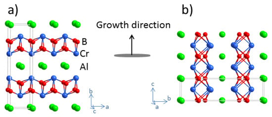
Figure 1.
Crystal structure of Cr2AlB2 showing the CrB slabs separated by Al layers. Sputtering of a thin film with an [010] orientation will expose Al layers to the plasma (a) while a film growing with a strong [100]/[001] texture will expose a mixed Al-Cr-B surface to the plasma (b).
The M2AlB2 phases have interesting magnetic and mechanical properties. Fe2AlB2, for example, is ferromagnetic with a Curie temperature close to room temperature. This phase has been suggested as a potential material for magnetic refrigeration due to its magnetocaloric properties [10]. In contrast, Mn2AlB2 is antiferromagnetic, while solid-solutions mixing Mn and Fe on the metal sites give a disordered ferrimagnetic phase [11]. In the Cr-Al-B system, three phases in the series (CrB2)nCrAl with n = 1, 2, 3 have been synthesised [8]. The boron network in Cr2AlB2, and in the other M2AlB2 phases, forms single zigzag chains with each B atom coordinated to six Cr atoms in a triangular prism as in CrB. On the other hand, double and triple chains of boron atoms in graphite-like layers are formed in Cr3AlB4 and Cr4AlB6, respectively, as observed in Cr3B4 and Cr2B3. A large increase in hardness was also reported as the boron content increased from Cr2AlB2 to Cr3AlB4. Furthermore, the similarities to MAX phases suggest that they have the potential to exhibit special deformation behaviour with kink bands observed in many MAX compounds. Initial deformation studies show indeed a delamination behaviour during deformation but not as pronounced as for e.g., Ti3AlC2 [7]. Further studies, however, are required to clarify the deformation behaviour of the M2AlB2 phases.
The M2AlB2 phases are easily synthesised as bulk materials by solid-state sintering or arc-melting followed by an annealing step, in both cases with an excess of Al. Hitherto, however, no studies on the deposition of these compounds as thin films have been published. The similarities to MAX phases and MoAlB suggest that a rather high deposition temperature is required but the complex structure and difficulties associated with the thin film deposition of metal boride compounds are challenging. The aim of this study is to deposit single-phase Cr2AlB2 films and to identify important process parameters to obtain well-defined films. Establishment of such parameters could also facilitate the deposition of dense films of magnetocaloric Fe2AlB2, with potential applications in microscale refrigeration and other MAB phases.
2. Materials and Methods
Initial attempts to deposit Cr2AlB2 films with conventional magnetron sputtering from Al, Cr and B targets at different process parameters were unsuccessful. A combinatorial approach was therefore used with three magnetrons and a non-rotating substrate. On a large substrate this will, in a single experiment, generate a film with a compositional gradient enabling a rapid screening of the parameter space. All films were deposited in an ultra-high vacuum chamber with the magnetrons symmetrically spaced at 39° with respect to the sample surface normal. The target to substrate distance was 17.5 cm at the focus point. The lowest base pressure that could be achieved at room temperature was 8 × 10⁻⁹ Pa after sputtering a titanium target for 3 h. The targets used in the depositions were a composite target of aluminum and boron, bonded with indium to a copper backing plate (SCM, assayed composition AlB2 with 99.9% purity), and Al and Cr targets (Lesker, >99.95% purity) with 3′ diameter. The substrates used were 3′ Si (100) wafers and 10 × 10 mm2 MgO (100) or Al2O3 (001) that had been ultrasonically cleaned in both ethanol and isopropanol for 10 min. The substrates were heated at 600 °C for 30 min prior to depositions and a seed layer of Cr of about 5–10 nm was deposited on the single crystal substrates while rotating the substrate holder at the deposition temperature. Depositions were made using 6 N grade Ar as a sputtering gas at a pressure of 0.27 Pa. No bias was applied to the substrate which was kept floating. In order to avoid arcing, the composite Al-B target was sputtered using an RF power supply (AE RFX-600, Advanced Energy Industries, Inc., Denver, CO, USA) with a matching network at 170 W. The low deposition rate obtained from this target was a limiting factor and the Cr target was sputtered using a pulsed DC power supply (AE Pinnacle Plus 5 kW) at the lowest possible power (15 W) required to maintain a stable plasma at 250 kHz with a 1.6 μs pulse factor. The Al-B and Cr targets were mounted on magnetrons opposite each other to obtain a compositional gradient and an Al target was mounted at 90° from this axis and sputtered using a DC power supply (AE MDX-500, Advanced Energy Industries, Inc., Denver, CO, USA) at 15 W in power regulation. The deposition time for the films prepared at 680 °C was 6 h.
The phase composition of the films grown on MgO substrates was investigated with X-ray diffraction (XRD) using a Bruker D8 diffractometer with CuKα1 radiation (λ = 1.54056 Å). Film thicknesses were obtained from analysis of X-ray reflectivity (XRR) data collected using a Phillips MRD X’Pert diffractometer with CuKα radiation. Microscopy studies were carried out with a Zeiss LEO-1550 scanning electron microscope (SEM) (ZEISS, Oberkochen, Germany) equipped with an AZtec energy dispersive X-ray detector for spectroscopy analysis (EDS) at an acceleration voltage of 10 kV. The chemical composition was investigated by X-ray photoelectron spectroscopy (XPS) using a Physical Systems Quantum-2000 spectrometer (Physical Electronics, Inc., Eden Prairie, MN, USA) with Al Kα radiation. Depth profile analyses were performed on a spot of 200 μm after pre-sputtering for 10 min using a 1 kV Ar+ ion beam. Prior to the sputtering, the peak position of the C 1s peak was centered at 284.8 eV and no surface charge neutralisation was used. The sensitivity factors used for Al and Cr were those included in the MultiPak v9.0 software database [12], while the sensitivity factor for B was corrected for matrix effects using spectra collected on a CrB2 thin film.
Cross-section samples of the films deposited on MgO for transmission electron microscopy (TEM) analysis were prepared with a focused ion beam and scanning electron microscope (FIB-SEM, FEI Strata DB-235, FEI Company, Hillsboro, OR, USA). The samples were transferred to a Cu lift-out grid and thinned to electron transparency applying a final polishing step using 5 kV Ga ions. TEM analysis was carried out on a probe corrected FEI Titan Themis equipped with the SuperX system for EDS analysis (FEI Europe B.V., Eindhoven, The Netherlands). The acquired EDS elemental maps were recorded and quantified with Esprit 1.9 from Bruker using the theoretical k-factors provided by the software. Electron diffraction studies were carried out in nano-beam (NBD) mode with a lateral resolution of ca 2.5 nm. The electron diffraction patterns were evaluated with the CrystBox software suite [13].
3. Results
In an initial series of experiments, attempts were made to deposit single-phase AlB2 at 430 °C on Si substrates from the Al-B target to identify suitable deposition conditions for the ternary Cr2AlB2 phase. XPS analysis showed an Al/B ratio of 0.2 instead of the expected 0.5 ratio of AlB2. This could be partly due to a lower Al content in the Al-B target than the assayed value. Furthermore, it is reasonable to assume that a significant loss of Al can occur from the growing film at higher temperatures. An additional Al target was therefore used in all other depositions. The deposition rate obtained from the Al-B target with the RF power supply at 170 W was 0.5 nm/min. The sputtering rate of the Al target at 15 W was determined to 0.75 nm/min and co-sputtering with the Al target increased the Al/B ratio to 0.67 at a position on the compositional gradient close to the Al target and 0.46 close to the Al-B target. Thus, a stoichiometry with elemental boron and aluminium close to AlB2 is expected at a position between the Al and Al-B targets. Co-sputtering of the Al, Al-B and Cr targets was done using the same settings on the Al and Al-B targets previously determined to give an Al/B ratio close to 0.5 as described above. The sputtering rate from the Cr target was reduced by using a pulsed DC source at a low power (15 W) which resulted in a growth rate of 1.3 nm/min.
Using the sputtering parameters described above, a compositional gradient film was deposited on a Si wafer at 430 °C. The film shows a darker region close to the Al-B target and a completely metallic luster close to the Cr target (Figure 2a). XPS analyses were carried out at three different positions labelled A, B and C in Figure 2a, which are the extreme points of the wafer giving Al rich, Cr deficient and Al deficient compositions respectively. The position closest to the Cr target was found to have a high Cr content and was not considered further. The compositions obtained at these positions are given in Figure 2c and marked in the ternary Cr-Al-B phase diagram in Figure 2b.
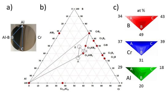
Figure 2.
(a) Image of the Si wafer with a compositional gradient with labels showing where the XPS analyses were performed and the orientation of the targets. (b) Ternary Cr-Al-B section with known binary and ternary phases (adapted from [15]) marked with red dots. The analysis spots are marked with circles and Al, CrB2 and Cr2AlB2 compositions are joined by lines. (c) Measured compositions in the Cr-Al-B gradient at points A, B and C in at.%. The vertex pointing down shows the composition at point B, while the vertices to the left and right show compositions A and C, respectively.
X-ray diffraction patterns at different positions on the film deposited at 430 °C were X-ray amorphous except for in the Al rich part of the film where peaks from Al and Cr4Al13Si4 were observed. The formation of chromium silicides would be expected at higher temperatures [14] but it is likely that this ternary phase is more stable at these conditions. This suggests a reaction with the Si substrate and therefore subsequent experiments were carried out on MgO and Al2O3 substrates placed at positions A, B and C as shown in Figure 2a. To increase the crystallinity of the films, deposition experiments were carried out at 550 °C. XRD showed the formation of Al and CrB2 but no indication of a ternary phase. The deposition temperature was therefore increased to 680 °C, above the melting point of Al (660 °C), and depositions were made on both MgO and Al2O3 substrates. At this temperature, the formation of Cr2AlB2 was observed only on MgO substrates and the diffraction patterns of three films deposited on MgO substrates at positions A, B and C are shown in Figure 3.
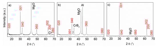
Figure 3.
θ–2θ X-ray diffraction scans (λ = 1.5406 Å) collected on films grown on MgO substrates placed (a) close to the Al target at position A, (b) close to the Al-B target at position B (with a small peak from the (030) reflection of Cr3AlB4 indicated by a star), (c) far from the Al target at position C (with the MgO peak masked).
The diffraction pattern from the film deposited at position C shows only reflections from the Cr2AlB2 phase (Figure 3c). As indicated in Figure 2b, position C is indeed close to stoichiometric Cr2AlB2. Sharp diffraction peaks with high intensity originate from (00l) reflections. Due to the reflection conditions in the Cmmm space group with c > a, the (h00) reflection with h = 2n is indicated but has a weak intensity. This suggests that the Cr2AlB2 film grows with a strong [00l] preferred orientation in this sample. The diffraction pattern obtained from the film deposited at position A shows sharp (00l) reflections but also strong (0k0) peaks from the ternary Cr2AlB2 phase suggesting a [0k0] texture in addition to the [00l] orientation. A weak (200) peak of Cr is also observed in this diffraction pattern. Cell parameters for the Cr2AlB2 phase deposited at position A were determined from a diffraction pattern using grazing incidence XRD (not shown) to be a = 2.9371(1) Å, b = 11.0913(4) Å and c = 2.9597(1) Å. These are in good agreement with the experimental data obtained from bulk samples [8]. An XPS analysis of this film was carried out to confirm the chemical composition. The oxygen content of the film was very high (18 at.%). This can be explained by the chimney-like morphology of the grains (described below), which exposes a large surface area of the film to air. After removal from the deposition chamber, the exposed surface will oxidise giving a very thin surface oxide. This oxide can only partly be removed from a rough surface with Ar+ ion beam sputtering. Therefore, the main source of oxygen in this case is the post-oxidation of the sample after being exposed to air. From the areas of the Cr 2p3/2, B 1s and Al 2s peaks, the chemical composition of sample A is determined to be Cr0.38Al0.26B0.36 (excluding oxygen), i.e., with the correct Cr/B ratio but a higher Al content than in Cr2AlB2. This is expected since this film is deposited closer to the Al target.
The diffraction pattern from the film deposited at position B, closer to the Al-B target, showed a more complex phase composition. The observed diffraction peaks were assigned to pure Al and hexagonal CrB2, from their respective (200) and (100) reflections, Cr2AlB2 and a weak peak from another ternary phase, Cr3AlB4. The latter is a thermodynamically stable phase present in the published phase diagrams [15] and marked in Figure 2b. The fact that we have four phases present suggests that the films are deposited at non-equilibrium conditions. The composition obtained by XPS in this sample (excluding oxygen) is determined to be Cr0.36Al0.18B0.46. In this case, a lower oxygen content after sputtering (8 at.%) was obtained. The lower oxygen content in this film can be explained by the smoother surface morphology shown in Figure 4. In summary, the XPS and XRD analyses show that the compositions and phases at positions A, B and C are found within the triangle defined by Cr2AlB2, CrB2 and Al shown in Figure 2b.
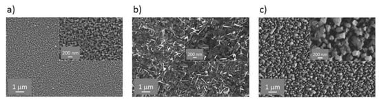
Figure 4.
SEM images of samples at position A (a), position B (b) and position C (c) with high-magnification images as insets.
Figure 4 shows SEM top view images from the films deposited at positions A, B and C. The two positions A and C, which according to XRD only consist of Cr2AlB2, exhibit a columnar microstructure with chimney-like outgrowths (Figure 4a,c). The grains at position A (closer to the Al target) do not show coalescence but are significantly smaller than at position C. In contrast, the film at position B exhibits a completely different morphology. The inset in Figure 4b shows cuboid grains with a small number of whisker-like outgrowths.
The films deposited at positions A and B were studied in more detail with TEM. Combining the EDS and image information for sample A, four different structural features can be distinguished in Figure 5a. At the interface to the MgO substrate, a thin layer (≈18 nm) of pure Al is formed, which is interrupted by smaller patches of pure Cr (the boron signal in this area is noise). This Al layer is probably too thin to be detected in the X-ray diffraction pattern in Figure 3a. Then, two features with the same composition but with two different growth modes are observed. The first growth mode is a rougher area composed of an arrangement of flat, plate-like grains and the second a columnar structure with crystals up to 500 nm in length perpendicular to the substrate. These chimney-like outgrowths are also seen in the inset in Figure 4a. The fourth feature is material between the columns that show an increased Al and lower Cr and B content.
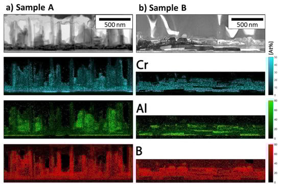
Figure 5.
Scanning TEM (STEM) bright field images of sample A (a) and B (b) with corresponding EDS maps.
For sample B, three different features can be distinguished (Figure 5b). The first feature is grains of pure Al. The second are grains containing Al, Cr and B with similar concentration as in sample A. Grains that contain no Al and show a high B to Cr ratio are also observed. Quantification with EDS is not very accurate, especially for materials containing light elements such as boron. To identify the phases, the films were probed using NBD and atomically resolved STEM. Figure 6 shows high-angle annular dark field images (HAADF) and NBD patterns from sample A. All zone axis patterns can be indexed with the Cr2AlB2 structure and are aligned with the [100] MgO substrate orientation. For the plate-like grains close to the substrate, the [101] zone axis is observed (Figure 6d) and the b-direction is perpendicular to the surface, meaning that the CrB slabs are oriented parallel to the substrate interface (the orientation in Figure 1a). The atomic arrangement is shown in the atomically resolved HAADF STEM image in Figure 6b. For the chimney-like grains, two different Cr2AlB2 orientations aligned with the [100] MgO substrate orientation are detected: the [014] and [3–10] zone axes, shown in Figure 6e,f respectively. The atomic model of the [014] orientation is overlaid with the HAADF STEM image in Figure 6c with the a-axis oriented perpendicular to the surface. For the [3–10] orientation, the c-axis is aligned perpendicular to the surface (the orientation shown in Figure 1b). This texture is also observed by the strong (001) reflection in the X-ray diffraction pattern of sample A.
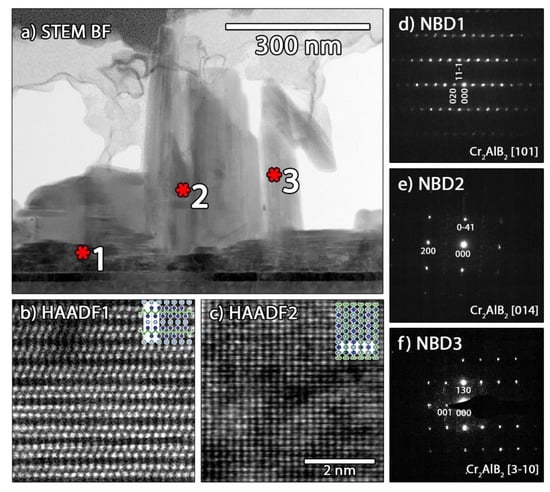
Figure 6.
TEM analysis of different growth modes in sample A: (a) bright field STEM image with marked positions for structural analysis, (b,c) atomic resolution high-angle annular dark field images (HAADF) STEM image of [101] and [014] zone axis orientation recorded at spots 1 and 2, respectively, as marked in (a), the same scale bar applies in (b,c). (d,e) NBD patterns of [101], [014] and [3–10] zone axis orientation recorded at spots 1, 2 and 3, respectively, as marked in (a).
For sample B, the three chemically different grains were probed with NBD and HAADF STEM to identify the structures present. The small Cr3AlB4 impurity that was identified in the X-ray diffractogram was not found in this TEM analysis. However, it is likely that this phase would form at the interface between Cr2AlB2 and CrB2 grains. All zone axis patterns are aligned with the [110] orientation of the MgO substrate. Figure 7a shows the bright field STEM overview with the positions where the NBD patterns and high resolution HAADF STEM images, as depicted in Figure 7b–d and Figure 7e–g, respectively, were recorded. The NBD pattern recorded at spot 1 is indexed with the Cr2AlB2 structure in [001] orientation with the b-axis perpendicular to the surface, which is verified by the STEM HAADF image in Figure 7e. The NBD patterns taken at spots 2 and 3 identify the grains as CrB2 with the [001] orientation and Al with the [110] orientation, respectively. The formation of Cr2AlB2, CrB2 and Al grains is also confirmed by the EDS maps in Figure 5b and their orientation relationship can be determined from the electron diffraction patterns. Thus, the Cr2AlB2 (200), the CrB2 (1–20) and the Al (−220) reflections marked in Figure 7b–d coincide. These correspond to aligned lattices with spacings of 1.4315, 1.4860 and 1.4686 Å in the ideal structures, respectively. The main orientation is given by the MgO substrate with the coinciding (−220) reflection (d = 1.4889 Å), leading to an apparent epitaxial growth and a small lattice mismatch of <4%.
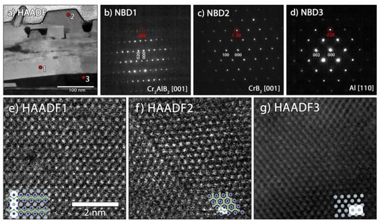
Figure 7.
TEM analysis of sample B: (a) dark field STEM image with marked positions for structural analysis, (b) NBD pattern of Cr2AlB2 in [001] orientation, (c) of CrB2 in [001] orientation and (d) of Al in [110] orientation recorded at spots 1, 2 and 3, respectively, as marked in (a) with the reflections encircled in red indicating coinciding reflections, (e,f) atomic resolution HAADF STEM images corresponding to the NBD patterns in (b–d), respectively. The same scale bar applies in (e–g).
A high resolution XPS analysis was carried out for sample A. The B 1s spectrum in Figure 8a can be fitted with two peaks centered at 187.8 and 188.4 eV with FWHM of 1.0 eV that can be attributed to B-B and B-metal peaks respectively [16]. No indication of oxidised boron species at higher bonding energies was observed. In Figure 8b, the Cr 2p spectrum shows a single Cr 2p3/2 peak at 574.2 eV with a FWHM of 1.1 eV and the Cr 2p1/2 peakat 583.5 eV (E = 9.3 eV) that can be assigned to Cr-B bonds although no chemical shift is observed between the metallic and boride bonds [17]. Thus, to account for the measured oxygen content of 18 at.%, the absence of oxide peaks in the B and Cr spectra suggests the presence of oxidised Al. The Al 2p spectrum overlaps with the Cr 3s peak and displays an asymmetric peak at high binding energies. The analysis included a peak centered at 72.7 eV attributed to metallic Al and a peak at 73.9 eV that can be assigned to Al2O3, with their area ratio determined to be 15/85. The peak at higher binding energies in Figure 8c can be assigned to Cr 3s [18]. A similar shape for the Al 2p + Cr 3s peak has been observed in the related Cr2AlC compound where an oxygen content of 20 at.% was reported [19]. The Al 2s spectrum in Figure 8d was fitted with a peak for the Al-Al bonds centered at 117.8 eV and peak centered at 120.1 eV attributed to Al-O bonds. The fraction of metallic Al is approximately 0.17, i.e., in agreement with the value obtained from the Al 2p spectrum. Similar oxide contributions to the Al spectra have been determined from the analysis of bulk Cr2AlB2 samples [20].
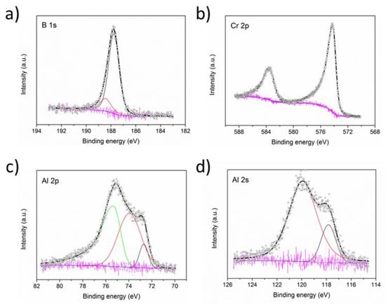
Figure 8.
XPS B 1s (a), Cr 2p (b), Al 2p (c) and Al 2s (d) spectra collected for sample A. The circles mark the raw intensities and the blue line the Shirley background. The peaks in colour indicate the fitted contributions with their sum in black and the difference to the raw data in pink. The green line in (c) represents the contribution of the overlapping Cr 3s peak.
4. Discussion
The results in Figure 3, Figure 4, Figure 5, Figure 6 and Figure 7 suggest a complex growth behaviour strongly dependent on the composition. XPS analyses show that the composite Al-B target used in this study is slightly sub-stoichiometric with respect to Al. An additional source of Al is therefore required to obtain the correct Al content for the deposition of Cr2AlB2. Crystalline films of the ternary phase are only observed at high temperatures (above the melting point of pure Al) and it is reasonable to assume that a loss of Al due to a higher vapour pressure continuously occurs during the growth process. A similar observation has been made for the deposition of V2AlC films from elemental targets [21]. Moreover, the synthesis of bulk MoAlB and M2AlB2 by different methods also requires excess Al due to the formation of Al-rich secondary phases [9]. Thin films of MoAlB have recently been deposited using combinatorial magnetron sputtering of MoB and Al targets on Al2O3 wafers at 700 °C [6]. Grazing incidence X-ray diffraction patterns showed the formation of MoAlB polycrystalline films with AlB2 as a second phase in Al-rich coatings. Moreover, a different texture was observed in the close to stoichiometric coating, which was partly attributed to changes in the chemical composition.
A loss of Al can explain the growth behaviour in positions A and C. As shown in the ternary phase diagram in Figure 2, position C has a composition close to Cr2AlB2 and the single-phase ternary film observed in the X-ray diffraction pattern is therefore in good agreement with thermodynamics. In a solid-state reaction, the formation of the ternary phase can be described as a topotactic reaction with the intercalation of Al between CrB layers [22]. However, during vapour deposition, Cr2AlB2 can expose two types of surfaces towards the vapour phase depending on the growth direction of the grains. The surface in the [010] direction has CrB slabs separated by layers of Al (Figure 1a). It is likely that such Al monolayers at 680 °C (above the melting point of Al) have high evaporation rates making it less favourable to grow grains with this texture. In contrast, grains with the [100] and [001] orientation expose the Al layers on the sides perpendicular to the growth direction (Figure 1b). It is conceivable to assume that the evaporation rate of Al from the (100) and (001) surface, where the Al is embedded between the CrB slabs, is lower than from the (010) surface. At position C, this should favour the formation of elongated and chimney-like grains with the [100]/[001] texture observed in Figure 4c. In sample A, the Al content is higher. In agreement with the XRD results in Figure 3a and the TEM results in Figure 5 and Figure 6, this would enable the formation of Cr2AlB2 grains with a [010] texture exposing Al layers to the vapour. In addition, according to the phase diagram in Figure 2, sample A is now on the tie line between Al and Cr2AlB2. The additional Al can probably be found in the amorphous features, rich in Al, between the columns seen in Figure 5a. Both types of grains would be easily oxidised after exposure to air and account for the measured oxygen content in XPS analyses. A thin layer of Al is also formed at the film/substrate interface in sample A. It is unclear if this layer is formed at the initial stages of growth or is precipitated at a later stage from a more Al-rich film.
At position B, the boron content is higher and the composition will then move into the Cr2AlB2- CrB2-Al triangle as shown in Figure 2b. Interestingly, the XRD analysis in Figure 3 shows the simultaneous growth of the four phases in the marked Cr2AlB2-CrB2-Al triangle. As only three phases can be in equilibrium in a ternary system, the triangle does not illustrate the equilibrium conditions for sample B, where at 800 °C a three-phase region exists between Al, Cr2AlB2 and Cr3AlB4 [15]. In this sample, the different phases are present as rather large grains at different parts of the film that grow with a close lattice matching of distinct crystallographic orientations coherent with the (100) plane of the MgO substrate.
Lastly, it is important to emphasise that the deposition conditions applied in this study have been obtained using a combinatorial approach. The use of elemental targets in the deposition of multi-element thin films requires the tuning of several parameters and a large number of experiments as only one composition is deposited on a rotating substrate in each experiment. The combinatorial sputtering approach is an established method for the rapid preparation of compositional gradients on a stationary substrate for the analysis of different properties on a continuous gradient. However, the advantage of obtaining a large compositional gradient has some drawbacks. Possible shadowing effects can be caused by the deposition at an oblique angle on a stationary substrate. Also, the measured composition will be an average and on a larger scale, the thickness of the film will vary across the gradient and influence the physical properties at different points, which limit the use of gradient films in practical applications.
5. Conclusions
In this work, films of Cr2AlB2 have been deposited for the first time using a combinatorial sputtering approach. Cr2AlB2 is a nanolaminated MAB phase with structural similarities to the well-known MAX phases. The structure can be described as CrB slabs separated by monolayers of Al, where the strong Cr-B and the weaker Cr-Al bonds give rise to the laminated structure. The results in this study show that it is difficult to deposit single-phase Cr2AlB2 films with a dense microstructure. A high temperature (above the melting point of Al) is required, leading to a loss of Al, which was compensated with an extra Al target. Depending on the Al content, different orientations of the ternary phase grains are obtained. [010] oriented grains with the CrB slabs parallel to the substrate were only observed with an excess of Al presumably due to a higher evaporation rate from [010] surfaces than from the surfaces of grains with a [100]/[001] orientation. To deposit dense single-phase Cr2AlB2 films we suggest that the deposition rate must be increased using a different target configuration and the temperature reduced using e.g., high-power impulse magnetron sputtering (HIPIMS). It is expected that these findings will facilitate the deposition of other MAB phases as thin films, including the ferromagnetic Fe2AlB2 phase, and fuel the search for other hitherto-unknown MAB phases using physical vapour deposition.
Author Contributions
Conceptualisation, U.J.; validation, P.B., L.R. and U.J.; formal analysis, P.B. and L.R.; investigation, P.B. and L.R.; writing—original draft preparation, P.B., L.R. and U.J.; visualisation, L.R. and P.B.; supervision, U.J.; funding acquisition, U.J. All authors have read and agreed to the published version of the manuscript.
Funding
This research was funded by the Swedish Research Council, grant No. 2014-05841.
Conflicts of Interest
The authors declare no conflict of interest.
References
- Barsoum, M.W.; Radovic, M. Elastic and mechanical properties of the MAX phases. Annu. Rev. Mater. Res. 2011, 41, 195–227. [Google Scholar] [CrossRef]
- Verger, L.; Natu, V.; Carey, M.; Barsoum, M.W. MXenes: An Introduction of their synthesis, select properties, and applications. Trends Chem. 2019, 1, 656–669. [Google Scholar] [CrossRef]
- Eklund, P.; Beckers, M.; Jansson, U.; Högberg, H.; Hultman, L. The M(n+1)AX(n) phases: Materials science and thin-film processing. Thin Solid Films 2010, 518, 1851–1878. [Google Scholar] [CrossRef]
- Bai, Y.L.; Qi, X.X.; Duff, A.; Li, N.; Kong, F.Y.; He, X.D.; Wang, R.G.; Lee, W.E. Density functional theory insights into ternary layered boride MoAlB. Acta Mater. 2017, 132, 69–81. [Google Scholar] [CrossRef]
- Alameda, L.T.; Moradifar, P.; Metzger, Z.P.; Alem, N.; Schaak, R.E. Topochemical deintercalation of Al from MoAIB: Stepwise etching pathway, layered intergrowth structures, and two-dimensional MBene. J. Am. Chem. Soc. 2018, 140, 8833–8840. [Google Scholar] [CrossRef] [PubMed]
- Achenbach, J.O.; Sahu, R.; Volker, B.; Hans, M.; Primetzhofer, D.; Miljanovic, D.J.; Scheu, C.; Schneider, J.M. Synthesis and properties of orthorhombic MoAlB coatings. Coatings 2019, 9, 510. [Google Scholar] [CrossRef]
- Kadas, K.; Iusan, D.; Hellsvik, J.; Cedervall, J.; Berastegui, P.; Sahlberg, M.; Jansson, U.; Eriksson, O. AlM2B2 (M = Cr, Mn, Fe, Co, Ni): A group of nanolaminated materials. J. Phys.Condens Matter 2017, 29, 155402. [Google Scholar] [CrossRef] [PubMed]
- Ade, M.; Hillebrecht, H. Ternary borides Cr2AlB2, Cr3AlB4, and Cr4AlB6: The first members of the series (CrB2)(n)CrAl with n = 1, 2, 3 and a unifying concept for ternary borides as MAB-phases. Inorg. Chem. 2015, 54, 6122–6135. [Google Scholar] [CrossRef] [PubMed]
- Kota, S.; Sokol, M.; Barsoum, M.W. A progress report on the MAB phases: Atomically laminated, ternary transition metal borides. Int. Mater. Rev. 2020, 65, 226–255. [Google Scholar] [CrossRef]
- Tan, X.Y.; Chai, P.; Thompson, C.M.; Shatruk, M. Magnetocaloric effect in AlFe2B2: Toward magnetic refrigerants from earth-abundant elements. J. Am. Chem. Soc. 2013, 135, 9553–9557. [Google Scholar] [CrossRef] [PubMed]
- Cedervall, J.; Andersson, M.S.; Iusan, D.; Delczeg-Czirjak, E.K.; Jansson, U.; Nordblad, P.; Sahlberg, M. Magnetic and mechanical effects of Mn substitutions in AlFe2B2. J. Magn. Magn. Mater. 2019, 482, 54–60. [Google Scholar] [CrossRef]
- PHI. Operator’s Multipak Software Manual; Physical Electronics Inc.: Eden Prairie, MN, USA, 2000. [Google Scholar]
- Klinger, M.; Jager, A. Crystallographic Tool Box (CrysTBox): Automated tools for transmission electron microscopists and crystallographers. J. Appl. Cryst. 2015, 48, 2012–2018. [Google Scholar] [CrossRef] [PubMed]
- Zalar, A.; Hofmann, S.; Pimentel, F.; Panjan, P. Interfacial Reactions and silicide formation in Si/Ni/Si and Si/Cr/Si sandwich layers. Surf. Interface Anal. 1994, 21, 560–565. [Google Scholar] [CrossRef]
- Guzei, L.S. Aluminum-Boron-Chromium. In Ternary Alloys; VCH: Weinheim, Germany, 1990; Volume 3, pp. 155–157. [Google Scholar]
- Nedfors, N.; Primetzhofer, D.; Wang, L.P.; Lu, J.; Hultman, L.; Jansson, U. Characterization of magnetron sputtered Cr-B and Cr-B-C thin films for electrical contact applications. Surf. Coat. Technol. 2015, 266, 167–176. [Google Scholar] [CrossRef]
- Zhang, S.C.; Wang, Z.Y.; Guo, P.; Ke, P.L.; Oden, M.; Wang, A.Y. Temperature induced superhard CrB2 coatings with preferred (001) orientation deposited by DC magnetron sputtering technique. Surf. Coat. Technol. 2017, 322, 134–140. [Google Scholar] [CrossRef]
- Kelly, D.; Jung, D.R. Elemental Chromium by XPS. Surf. Sci. Spectra 1998, 5, 130–137. [Google Scholar] [CrossRef]
- Obrosov, A.; Gulyaev, R.; Zak, A.; Ratzke, M.; Naveed, M.; Dudzinski, W.; Weiss, S. Chemical and morphological characterization of magnetron sputtered at different bias voltages Cr-Al-C coatings. Materials 2017, 10, 156. [Google Scholar] [CrossRef] [PubMed]
- Natu, V.; Kota, S.S.; Barsoum, M.W. X-ray photoelectron spectroscopy of the MAB phases, MoAlB, M2AlB2 (M = Cr, Fe), Cr3AlB4 and their binary monoborides. J. Eur. Ceram. Soc. 2020, 40, 305–314. [Google Scholar] [CrossRef]
- Sigumonrong, D.P.; Zhang, J.; Zhou, Y.C.; Music, D.; Schneider, J.M. Synthesis and elastic properties of V2AlC thin films by magnetron sputtering from elemental targets. J. Phys. D Appl. Phys. 2009, 42, 185408. [Google Scholar] [CrossRef]
- Lu, J.; Kota, S.; Barsoum, M.W.; Hultman, L. Atomic structure and lattice defects in nanolaminated ternary transition metal borides. Mater. Res. Lett. 2017, 5, 235–241. [Google Scholar] [CrossRef]


© 2020 by the authors. Licensee MDPI, Basel, Switzerland. This article is an open access article distributed under the terms and conditions of the Creative Commons Attribution (CC BY) license (http://creativecommons.org/licenses/by/4.0/).