Article

Experimental Study on the Thickness-Dependent Hardness of SiO2 Thin Films Using Nanoindentation

1
College of Science, Inner Mongolia University of Technology, Hohhot 010051, China
2
College of Arts and Sciences, Shanghai Maritime University, Shanghai 201306, China
3
Test Center, Inner Mongolia University, Hohhot 010051, China
*
Author to whom correspondence should be addressed.
These authors contributed equally to this work and should be considered co-first author.
Coatings 2021, 11(1), 23; https://doi.org/10.3390/coatings11010023
Submission received: 8 December 2020 / Revised: 21 December 2020 / Accepted: 24 December 2020 / Published: 27 December 2020
(This article belongs to the Special Issue Mechanical Properties of Advanced Multifunctional Coatings)

Abstract

:
SiO2 thin films are widely used in micro-electro-mechanical systems, integrated circuits and optical thin film devices. Tremendous efforts have been devoted to studying the preparation technology and optical properties of SiO2 thin films, but little attention has been paid to their mechanical properties. Herein, the surface morphology of the 500-nm-thick, 1000-nm-thick and 2000-nm-thick SiO2 thin films on the Si substrates was observed by atomic force microscopy. The hardnesses of the three SiO2 thin films with different thicknesses were investigated by nanoindentation technique, and the dependence of the hardness of the SiO2 thin film with its thickness was analyzed. The results showed that the average grain size of SiO2 thin film increased with increasing film thickness. For the three SiO2 thin films with different thicknesses, the same relative penetration depth range of ~0.4–0.5 existed, above which the intrinsic hardness without substrate influence can be determined. The average intrinsic hardness of the SiO2 thin film decreased with the increasing film thickness and average grain size, which showed the similar trend with the Hall-Petch type relationship.

1. Introduction

Due to its good chemical stability, optical properties, dielectric properties, abrasion resistance and corrosion resistance, silicon dioxide (SiO2) thin films have received intensive attention within the technology and scientific community [1,2,3,4,5,6,7,8,9], and are widely used in micro-electro-mechanical systems, integrated circuits and optical devices [10,11,12,13,14,15]. Tremendous efforts have been devoted to studying the preparation technology and optical properties of the SiO2 thin films [16,17,18,19], while little attention has been paid to their mechanical properties. In fact, the mechanical properties of SiO2 thin films can affect their optical and electrical properties, and can also affect the production yield, serving time and reliability of the SiO2 thin related devices [16,17,18,19,20,21,22]. Therefore, in order to optimize the design, and improve the performance, service time and reliability of the SiO2 thin film-related devices, the mechanical properties of SiO2 thin films should be studied carefully.
The nanoindentation technique has become an important means for characterizing the mechanical properties of films at micro- and nano-scale due to its high load resolution and displacement resolution [23,24,25,26]. Using the nanoindentation technique, we can determine many mechanical parameters such as hardness, elastic modulus, fracture toughness and so on [27,28,29,30]. In general, the penetration depth should be less than 10% of the film’s thickness in order to avoid the substrate effect in the nanoindentation test of the thin films [31].
The mechanical behavior of the SiO2 thin films has been studied by some researchers. Qin et al. [32] studied the influence of residual stress on the Young’s modulus determination for SiO2 thin film by the surface acoustic waves (SAWs), indicating which indicated that the influence of residual stress on the determination for SiO2 thin film by SAWs is small, and it can be ignored or revised. Rakshit et al. [33] measured in situ the stress evolution in SiO2 thin films in situ during electrochemical lithiation/delithiation cycling by monitoring the substrate curvature using a multi-beam optical sensing method, finding that upon lithiation, SiO2 undergoes extensive inelastic deformation, with a peak compressive stress of 3.1 GPa, and upon delithiation the stress becomes tensile, with a peak stress of 0.7 GPa. Ho et al. [34] quantified the mechanical adhesion of SiO2 thin films onto polymeric substrates by analyzing the SiO2 buckle morphologies generated under compressive stress. The impacts of the mechanical properties of SiO2 layers, as well as a surface pretreatment on adhesion, are shown. The interfacial toughnesses of both configurations are assessed using the Hutchinson and Suo model, which involves buckle dimensions determined in situ using an optical profilometer, and elastic modulus of the SiO2 thin films, characterized by nanoindentation. The surface pretreatment led to initiation of buckling at a higher strain. The same trend was observed for a layer with a lower stiffness and residual stress. Wang et al. [35] studied the substrate effects on the mechanical properties of SiO2 thin films deposited respectively on K9 and two different of Y3Al5O12 (YAG) crystals by nanoindentation and nanoscratch tests, showing that the Young’s moduli of all films were similar, the damage mechanisms of SiO2 thin films on K9 and YAG were different, and the adhesive forces of the film on the films on YAG (100) and YAG (111) were much less than homologous film on K9. Simurka et al. [36] investigated the mechanical properties of amorphous SiO2 films deposited on soda-line silicate float glass by reactive radio frequency magnetron sputtering at room temperature in dependence of the process pressure. As the pressure changed from 0.27 to 1.33 Pa, the residual compressive stresses in the deposited films varied in the range from 440 to 1 MPa. The hardness and reduced elastic modulus values followed the same trend and declined with the increase of process pressure from 8.5 to 2.2 GPa and from 73.7 to 30.9 GPa, respectively. However, these research works rarely involve investigation of the thickness-dependent hardness of SiO2 thin films using the nanoindentation technique.
Here, we present an experimental investigation of the thickness-dependent hardness of SiO2 thin films through nanoindentation technique and atomic force microscope (AFM). The surface morphology, load-penetration depth curves and hardnesses of the SiO2 films with different thicknesses were evaluated.

2. Theoretical Approach

The nanoindentation measurements were analyzed using the Oliver-Pharr method [37,38]. This technique continuously monitors the load (at load as low as a few μN) and the penetration depth (down to a few nanometers) of an indenter, usually of a Berkovich type, as it is pushed into and withdrawn from the surface of the sample. The hardness of the material is generally determined by dividing the peak load by the contact area at the projected residual contact area. The unloading curve is fitted with a power-law relationship:
P = α(hhf)m,
where P is the penetration load of indenter, h is the penetration depth, hf is the residual penetration depth after completely unloading, and α and m are fitting parameters. The contact depth, hc, can be estimated from the load-penetration depth data as:
hc = hmax − ε(Pmax/S),
where hmax is the maximum penetration depth at the peak load Pmax, ε is an indenter dependant constant, for a Berkovich indenter, ε = 0.75, S is the stiffness of the test material, and can be obtained from the initial unloading slope by evaluating the maximum load and maximum penetration depth, which is S = dP/dh. Hardness is defined as the resistance to local plastic deformation. It can be expressed as the maximum indentation load Pmax, divided by the projected contact area A:
H = Pmax/A,
where the projected contact area A is a function of the contact depth hc. For an ideal Berkovich indenter, the relationship between the projected contact area A and the contact depth hc is as follows:
A = 24.6hc2,

3. Experimental Details

The SiO2 films with different thicknesses used in this study were prepared by thermal oxidation of p-type (100) silicon wafers [39]. The silicon wafers were cut into 20 × 10 mm2 samples and cleaned to remove impurities and native oxide on the surface by using a conventional Radio Corporation of America (RCA) process and 1% HF. Then the cleaned samples were loaded into a quartz furnace at 600 °C and the temperature was ramped at a rate of 10 °C/min to reach an oxidation temperature of 1100 °C. This oxidation temperature was retained for 1 h, 3 h, and 10 h with water (H2O) vapor constantly flowing into the furnace. The vapor was formed ex situ by heating a bubbler containing deionized water at 95 °C. It was carried into the furnace by nitrogen (N2) carrier gas (250 mL/min), which was flown through the water. After the oxidation, a postoxidation annealing process was performed for 1 h at 1100 °C in ambient N2. Thus, three SiO2 films with thicknesses of 500, 1000 and 2000 nm were obtained.
The surface morphology and roughness of the three SiO2 thin films with different thicknesses were examined by using CSPM4000 atomic force microscopy (AFM) (Being Nano-Instruments, Ltd., Guangzhou, China). AFM measurements were performed at room temperature (25 °C) and a relative humidity of 50% in air. The AFM was used in tapping mode with the scan frequency of 5 Hz between the tip and the surface [40]. The scanning area was 7 × 7 μm2, and the AFM image size was 512 × 512 pixel2. The measurements were repeated three times for each SiO2 thin film on different scanning areas to validate the reproducibility of the data [41].
The mechanical properties of SiO2 films were investigated using a three-sided Berkovich diamond tip with the G200 Nano indenter (Aglient, SantaClara, CA, USA) at room temperature. The G200 Nano indenter had a maximum of 500 mN and a maximum indentation depth greater than 500 μm. With a load resolution of 50 nN and displacement resolution less than 0.01 nm, it could accurately test the mechanical behavior of the material at both the micro and nano scale. The nanoindentation measurements were conducted using continuous stiffness measurement procedures. The indentation loads acted on the film surface at a constant strain rate of 0.05 s−1 with different maximum penetration depths. When the penetration depth reached the maximum value, the corresponding peak load was held for 10 s and then unloaded at the same strain rate. Three test points at each maximum penetration depth were performed on the samples to confirm the reliability and repeatability of the nanoindentation tests. For the sake of eliminating interactions among the test points, the spacing between each pair of neighboring test points was set to 100 μm.

4. Results and Discussion

4.1. Morphology of the SiO2 Thin Films

Figure 1 illustrates the atomic force microscopy (AFM) two-dimension (2-D) and three-dimension (3-D) images of the 500-nm-thick, 1000-nm-thick and 2000-nm-thick SiO2 thin films. The surface roughness and average grain sizes of the three SiO2 thin films are also shown in Table 1. The values of the surface roughness (Ra), the root-mean-square (RMS) roughness and the height of irregularities at ten points (Rz) of the three SiO2 thin films with different thickness were in the order of nanometer, which indicated that all three SiO2 thin films have good smoothness, ensuring the accuracy and consistency of the nanoindentation experimental results.
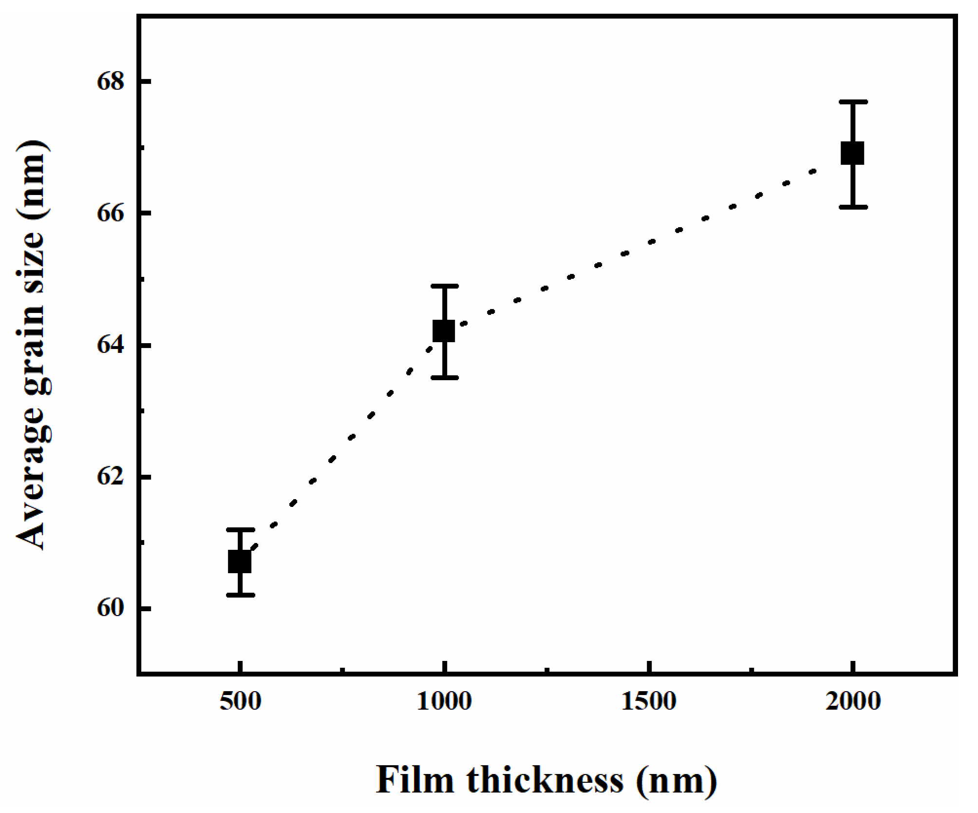
The average grain sizes of the 500-, 1000- and 2000-nm-thick SiO2 thin films were measured to be 60.7, 64.2 and 66.9 nm, respectively, and the corresponding change in the average grain size of the SiO2 films with respect to film thickness is shown in Figure 2. It can be seen that the average grain size of SiO2 thin film increases with increasing film thickness, which is because it is easier for atoms to migrate on the surface of the silicon wafer, and the islands are gradually connected according to the thin film growth diffusion principle.

4.2. Load-Penetration Depth Curves of the SiO2 Thin Films

Figure 3a–c show the dependence of load (P) with the penetration depth (h) and relative penetration depth (h/t, where t is the thin film thickness) at different maximum penetration depths for the 500, 1000 and 2000-nm-thick SiO2 thin films, respectively. It is observed that the P-h and P-h/t curves of the three test points at each maximum penetration depth hmax closely overlap for the three SiO2 thin films. Therefore, the load-penetration depth and relative penetration depth curves demonstrate a small variation and low noise, the experimental data have good repeatability, reliability and accuracy, and the three SiO2 thin films with different thicknesses have good uniformity.
As the hmax increases, the peak load Pmax gradually increases. It can be seen that the Pmax increased from 0.5 to 46.4 mN with the increasing hmax from 50 nm (1/10 of the film thickness) to 500 nm (film thickness) for the 500-nm-thick SiO2 thin film, the Pmax increased from 1.7 to 164.8 mN with the increasing hmax from 100 nm (1/10 of the film thickness) to 1000 nm (film thickness) for the 1000-nm-thick SiO2 thin film, and the Pmax increased from 5.7 to 642.1 mN with the increasing hmax from 200 nm (1/10 of the film thickness) to 2000 nm (film thickness) for the 2000-nm-thick SiO2 thin film.
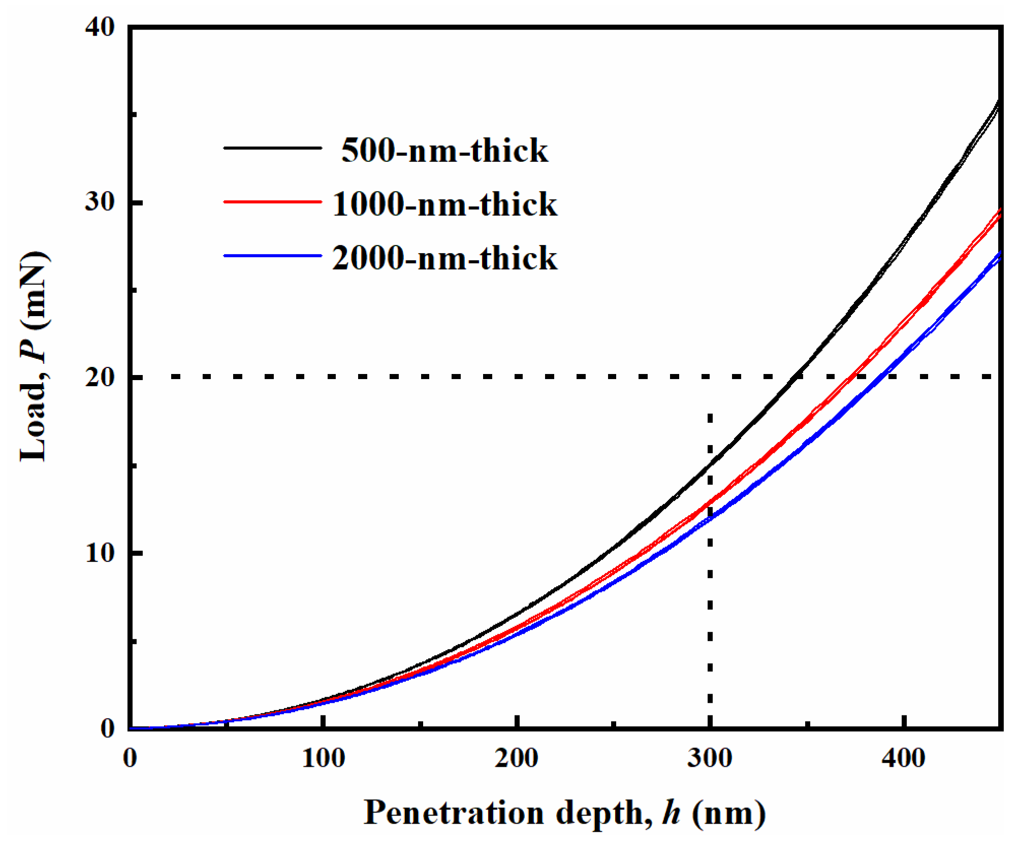
When the penetration depth reached the hmax, the corresponding peak load was held for 10 s and then unloaded. After unloading, penetration depth did not totally recover, and residual penetration depth remained, implying irreversible plastic deformation in SiO2 thin films with different thicknesses during the loading process. Part of the loading–penetration depth curves of the three SiO2 thin films with different thickness were extracted from Figure 3a–c, and shown in Figure 4. The loading curves of films with different thicknesses reflect the film’s ability to obstruct its own deformation and resist external pressure. It can be seen that at the same penetration depth, the load was the highest on the SiO2 film with a thickness of 500 nm, in the middle on the SiO2 film with the thickness of 1000 nm, and the lowest on the SiO2 film with the thickness of 2000 nm. Similarly, at the same load, the penetration depth was the lowest in the SiO2 film with the thickness of 500 nm, in the middle in the SiO2 film with the thickness of 1000 nm, and the highest in the SiO2 film with the thickness of 2000 nm. Therefore, the SiO2 film with the thickness of 500 nm has the highest resistance to external pressure, while the SiO2 film with the thickness of 2000 nm has the lowest.

4.3. Hardness of the SiO2 Thin Films

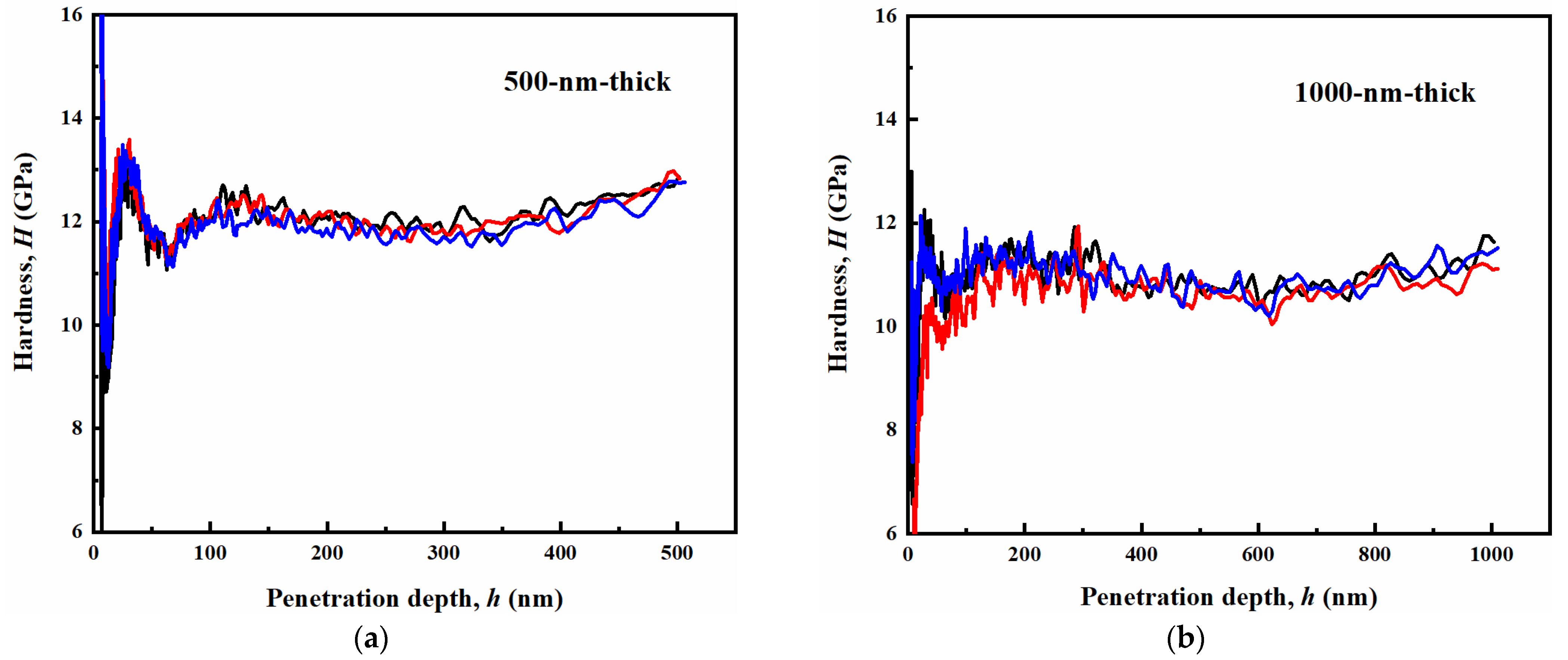
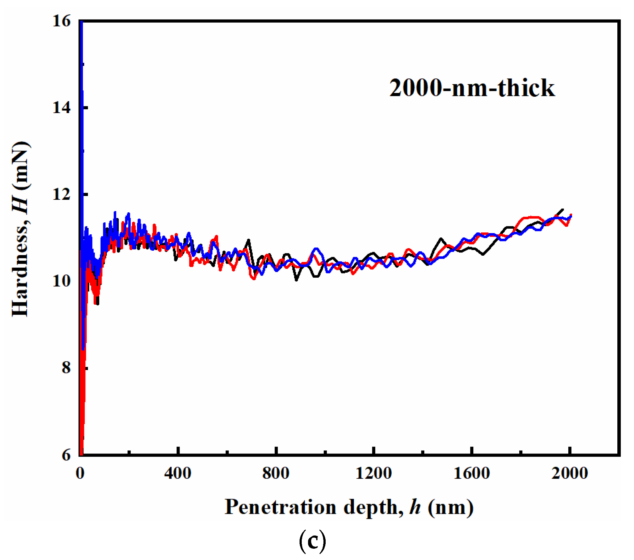
Figure 5a–c show the hardness–penetration depth curves of the 500-, 1000- and 2000-nm-thick SiO2 thin films when the maximum penetration depths reached the corresponding film thicknesses, respectively. For the 500-, 1000- and 2000-nm-thick SiO2 thin films, as the penetration depth was smaller than 100 nm, the data fluctuation was a bit high, which is probably associated with the resolution of the nanoindenter, the roughness of the sample surface, and ambient noise when searching for the initial contact position during the nanoindentation.
In Figure 5a, as the penetration depth increased from 100 to 200 nm, the hardness of the 500-nm-thick SiO2 thin film decreased slowly; as the penetration depth increased from 200 to 300 nm, the hardness tended to be stable; with increasing penetration depth more than 300 nm, the SiO2 thin film was affected by the substrate, and the hardness increased gradually. Therefore, in order to obtain the intrinsic hardness of 500-nm-thick SiO2 thin film without substrate influence, the penetration depth range should be ~200-300 nm. From Figure 5b,c, it can be seen that the hardnesses of the 1000- and 2000-nm-thick SiO2 thin films exhibited the similar trends with that of 500-nm-thick SiO2 thin film. To obtain the intrinsic hardnesses of 1000- and 2000-nm-thick SiO2 thin films without substrate influence, the penetration depth regions should be ~400–500 nm and ~900–1000 nm, respectively.
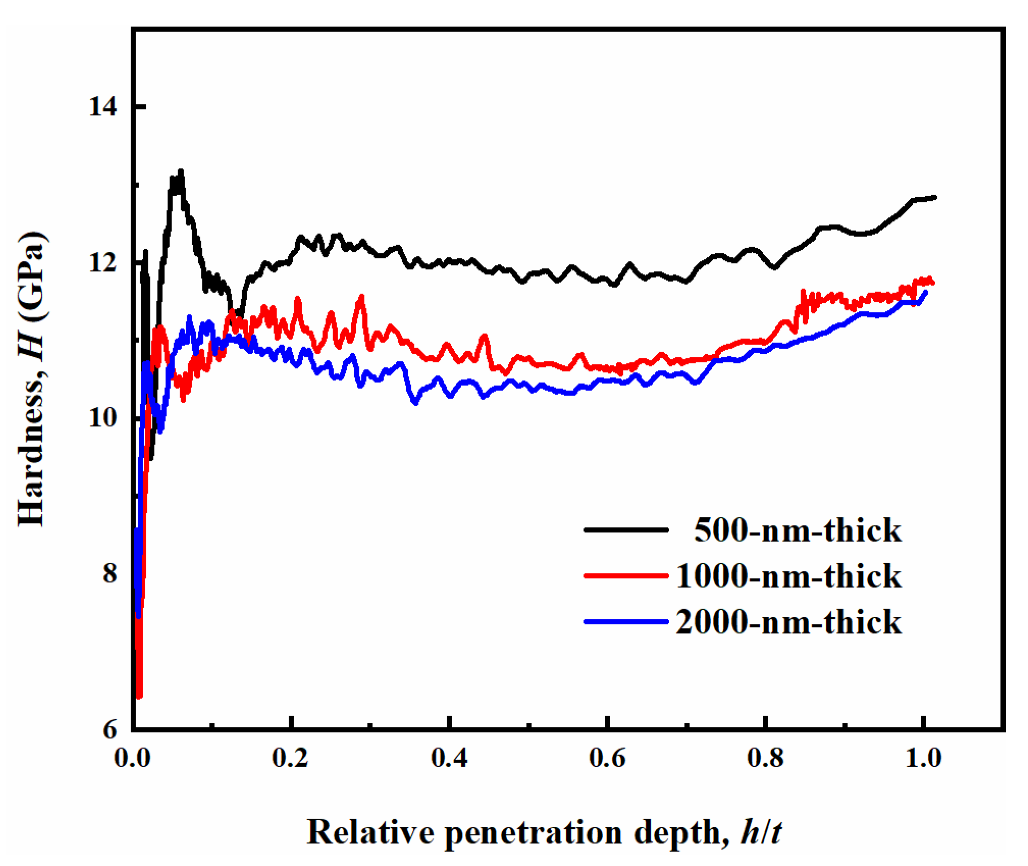
To compare the hardnesses of 500-, 1000- and 2000-nm-thick SiO2 thin films, the hardness was determined as the average of the values of three test points at each penetration depth. The corresponding hardness–relative penetration depth (H-h/t) curves of the 500-, 1000- and 2000-nm-thick SiO2 thin films are shown in Figure 6. It can be seen that, for the three SiO2 thin films with different thicknesses, the trends of hardness with the relative penetration depth were similar. The hardnesses of the three SiO2 thin films with different film thicknesses were stable in the same relative penetration depth range of ~0.4–0.5. Therefore, for the three SiO2 thin films, relative penetration depth ranges of ~0.4–0.5 existed, within which the intrinsic hardness could be determined without substrate influence.
It should be noted that the general rule that relative penetration depth should not exceed 0.1 in order to obtain an intrinsic hardness of the thin film in nanoindentation is not a universal law. In the case of a soft thin film on a hard substrate, due to the confinement of the plastic deformed volume by lateral spreading within the soft thin film, the relative penetration depth has been found to be greater than 0.1 [42,43,44].
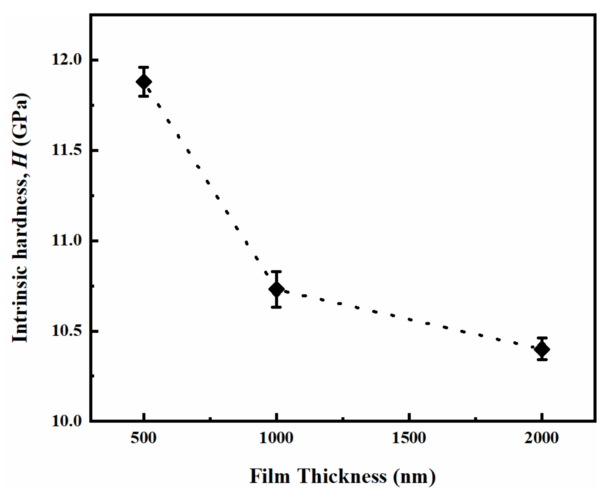
It also can be seen that the hardness of 500-nm-thick SiO2 thin film was greater than that of 1000- and 2000-nm-thick SiO2 thin films, and the hardness of 1000-nm-thick SiO2 thin film was a little greater than that of 2000-nm-thick SiO2 thin film. The average intrinsic hardnesses of the three SiO2 thin films with different film thicknesses were evaluated in the relative penetration depth range of 0.4–0.5. In addition, the average intrinsic hardnesses of the 500-, 1000- and 2000-nm-thick SiO2 thin films were 11.9, 10.7 and 10.4 GPa, respectively.
The dependence of the average intrinsic hardness of the SiO2 thin film on film thickness is shown in Figure 7. It can be seen that the average intrinsic hardness of the SiO2 thin film decreased with the increasing film thickness. As demonstrated in Figure 2, the average grain size of SiO2 thin film increased with the increasing film thickness. Therefore, the average intrinsic hardness of the SiO2 thin film decreased with the increasing average grain size (Figure 8). For the grain sizes of approximately 10–100 nm, Shockley partial dislocations or lattice dislocations that are nucleated in grain boundaries shear the grains and the dislocations are absorbed by the opposite grain boundaries. In this case, the hardness decreases with increasing grain size, namely, the Hall-Petch relationship holds [45,46,47,48,49]. Therefore, the results indicating that the average intrinsic hardness of the SiO2 thin film decreased with increasing film thickness exhibits a similar trend to that of the Hall-Petch type relationship.

5. Conclusions

The surface morphology, load–penetration depth curves and the hardnesses of the 500-, 1000- and 2000-nm-thick SiO2 thin films were investigated using the nanoindentation technique and force atomic force microscopy (AFM). The conclusions are as follows:
(1)
The values of surface roughness parameters (Ra, RMS and Rz) of the three SiO2 thin films with different thicknesses were in the order of nanometer, indicating that the three SiO2 thin films with different thicknesses had good smoothness, ensuring the accuracy and consistency of the nanoindentation experimental results. The average grain sizes of the 500-, 1000- and 2000-nm-thick SiO2 thin films were measured to be 60.7, 64.2 and 66.9 nm, respectively, indicating that the average grain size of SiO2 thin film increased with increasing film thickness.
(2)
The load–penetration depth curves of the three SiO2 thin films with different thicknesses demonstrate small variation and low noise, the experimental data have good repeatability, reliability and accuracy, and the three SiO2 thin films with different thicknesses have good uniformity. The SiO2 film with the thickness of 500 nm had the highest resistance to external pressure, while the SiO2 film with the thickness of 2000 nm had the lowest. Irreversible plastic deformation occurred in the three SiO2 thin films with different thicknesses during the nanoindentation process.
(3)
The average intrinsic hardnesses of the 500-, 1000- and 2000-nm-thick SiO2 thin films were 11.9, 10.7 and 10.4 GPa, respectively. The average intrinsic hardness of the SiO2 thin film decreased with increasing film thickness and average grain size, exhibiting a similar trend to the Hall-Petch type relationship.

Author Contributions

Conceptualization, J.L., W.Z., and Y.X.; methodology, J.L., W.Z., and X.N.; software, J.L., W.Z., and X.H.; validation, J.L., W.Z., and S.Y.; formal analysis, J.L. and W.Z.; investigation, J.L. and W.Z.; resources, J.L.; data curation, J.L., F.L., and W.Z.; writing—original draft preparation, J.L. and W.Z.; writing—review and editing, C.Z. and Y.X.; visualization, W.Z.; supervision, J.L. and Y.X.; project administration, J.L.; funding acquisition, J.L. and Y.X. All authors have read and agreed to the published version of the manuscript.

Funding

This research was funded by the National Science Foundation of China (Grant Nos. 11562016, 11972221, 12002174, 11762013, and 11762014), the Natural Science Foundation of Inner Mongolia Autonomous Region (Grant Nos. 2018MS01013 and 2013MS0107), and the Science Research Project of Inner Mongolia University of Technology (Grant Nos. X201713 and ZZ201812).

Data Availability Statement

Data is contained within the article.

Conflicts of Interest

The authors declare no conflict of interest.

References

  1. He, P.; Wang, C.; Li, C.; Yang, J.; Qiu, F.; Wang, R.; Yang, Y. Optical properties of the low-energy Ge-implanted and annealed SiO2 films. Opt. Mater. 2015, 46, 491–496. [Google Scholar] [CrossRef]
  2. Bose, S.; Cunha, J.M.V.; Suresh, S.; Wild, J.D.; Lopes, T.S.; Barbosa, J.R.S.; Silva, R.; Borme, J.; Fernandes, P.A.; Vermang, B.; et al. Optical lithography patterning of SiO2 layers for interface passivation of thin film solar cells. Sol. RRL 2018, 2, 1800212. [Google Scholar] [CrossRef]
  3. Zukowski, P.; Koltunowicz, T.N.; Czarnacka, K.; Fedotov, A.; Tyschenko, I.E. Carrier transport and dielectric permittivity of SiO2 films containing ion-beam synthesized InSb nanocrystals. J. Alloys Compd. 2020, 846, 156482. [Google Scholar] [CrossRef]
  4. Huang, C.; Lin, Y. Surface properties of SiO2 with and without H2O2 treatment as gate dielectrics for pentacene thin-film transistor applications. Chem. Phys. Lett. 2018, 691, 141–145. [Google Scholar] [CrossRef]
  5. Li, W.; Mu, C. Charging effects of SiO2 thin film on Si substrate irradiated by penetrating electron beam. Micron 2021, 140, 102961. [Google Scholar] [CrossRef] [PubMed]
  6. Qin, F.; Jiang, L.; Long, P.; Xu, S.; Ling, Y.; Yu, Y.; Wei, G. Effect of deposition potential on preparation and corrosion resistance of SiO2 film on copper. Int. J. Electrochem. Sci. 2020, 15, 6478–6487. [Google Scholar] [CrossRef]
  7. Mazur, A.; Checmanowski, J.G.; Szczygiel, B. The effect of SiO2 thin films deposited on the sol-gel method on steel 316L on its corrosion resistance and bioactivity in artificial blood solution. Przem. Chem. 2017, 96, 1183–1188. [Google Scholar]
  8. Lu, J.; Xu, Y.; Zhang, Y.; Xu, X. The effects of SiO2 coating on diamond abrasives in sol-gel tool for SiC substrate polishing. Diam. Relat. Mater. 2017, 76, 123–131. [Google Scholar] [CrossRef]
  9. Chen, A.; Chen, Y.; Wang, Y.; Qin, J. Silica abrasives containing solid cores and mesoporous shells: Synthesis, characterization and polishing behavior for SiO2 film. J. Alloys Compd. 2016, 663, 60–67. [Google Scholar] [CrossRef]
  10. Vanheusden, K.; Warren, W.L.; Devine, R.A.B.; Fleetwood, D.M.; Schwank, J.R.; Shaneyfelt, M.R.; Winokur, P.S.; Lemnious, Z.J. Non-volatile memory device based on mobile protons in SiO2 thin films. Nature 1997, 386, 587–589. [Google Scholar] [CrossRef]
  11. Lin, Y.; Hung, C.; Huang, J.; Lin, S.; Chang, H. Electrical and surface properties of SiO2 films modified by ultraviolet irradiation and used as gate dielectrics for pentacene thin-film transistor applications. Chin. J. Phys. 2019, 61, 248–254. [Google Scholar] [CrossRef]
  12. Choi, Y.; Bae, S.; Kim, J.; Kim, E.; Hwang, H.; Park, J.; Yang, H.; Choi, E.; Hwang, J. Robust SiO2 gate dielectric thin films prepared through plasma-enhanced atomic layer deposition involving di-sopropylamino silane (DIPAS) and oxygen plasma: Application to amorphous oxide thin film transistors. Ceram. Int. 2018, 44, 1556–1565. [Google Scholar] [CrossRef]
  13. Wu, F.; Si, S.; Shi, T.; Zhao, X.; Liu, Q.; Liao, L.; Lv, H.; Long, S.; Liu, M. Negative differential resistance effect induced by metal ion implantation in SiO2 film for multilevel RRAM application. Nanotechnology 2018, 29, 054001. [Google Scholar] [CrossRef] [PubMed]
  14. Wostbrock, N.; Busani, T. Stress and refractive index control of SiO2 thin films for suspended waveguides. Nanomaterials 2020, 10, 2105. [Google Scholar] [CrossRef] [PubMed]
  15. Pfeiffer, K.; Shestaeva, S.; Bingel, A.; Munzert, P.; Ghazaryan, L.; Helvoirt, C.V.; Kessels, W.M.M.; Sanli, U.T.; Grévent, C.; Schütz, G.; et al. Comparative study of ALD SiO2 thin films for optical applications. Opt. Mater. Express 2016, 2, 660–670. [Google Scholar] [CrossRef] [Green Version]
  16. Ullah, A.; Wilke, H.; Memon, I.; Shen, Y.; Nguyen, D.T.; Woidt, C.; Hillmer, H. Stress relaxation in dual ion beam sputtered Nb2O5 and SiO2 thin films: Application in a Fabry-Pérot filter array with 3D nanoimprinted cavities. J. Micromech. Microeng. 2015, 25, 055019. [Google Scholar] [CrossRef]
  17. Sun, Q.; Sun, D.; Shang, H.; Yu, T.; Chang, L.; Sun, Z.; Xing, W.; Dong, M. Study of birefringence and stress distribution of SiO2 film optical waveguide on silicon wafer. Coatings 2019, 9, 316. [Google Scholar] [CrossRef] [Green Version]
  18. Hasunuma, R.; Kawamura, H.; Yamabe, K. Reliability factors of ultrathin dielectric films based on highly controlled SiO2 films. Jpn. J. Appl. Phys. 2018, 57, 06KB05. [Google Scholar] [CrossRef]
  19. Revilla, R.I.; Li, X.; Yang, Y.; Wang, C. Large electric field-enhanced-hardness effect in a SiO2 film. Sci. Rep. 2014, 4, 4523. [Google Scholar] [CrossRef] [Green Version]
  20. Jeffery, S.; Sofield, C.J.; Pethica, J.B. The influence of mechanical stress on the dielectric breakdown field strength of thin SiO2 films. Appl. Phys. Lett. 1998, 73, 172–174. [Google Scholar] [CrossRef]
  21. Yamabe, K.; Liao, K.; Minemura, H.; Murata, M. Nonuniform distribution of trapped charges in electron injection stressed SiO2 films. J. Electrochem. Soc. 2001, 148, F9–F11. [Google Scholar] [CrossRef]
  22. Yang, T.; Saraswat, K.C. Effect of physical stress on the degradation of thin SiO2 films under electrical stress. IEEE Trans. Electron Dev. 2000, 47, 746–755. [Google Scholar] [CrossRef]
  23. Guo, Y.; Staedler, T.; Fu, H.; Heuser, S.; Jiang, X. A novel way to quantitatively determine the mechanical properties of thin films from the initial-grown surface by nanoindentation. Appl. Surf. Sci. 2019, 479, 253–259. [Google Scholar] [CrossRef]
  24. Broitman, E.; Tengdelius, L.; Hangen, U.D.; Lu, J.; Hultman, L.; Hoögberg, H. High-temperature nanoindentation of epitaxial ZrB2 thin films. Scripta Mater. 2016, 124, 117–120. [Google Scholar] [CrossRef] [Green Version]
  25. Wang, Y.; Zhang, J.; Wu, K.; Liu, G.; Kiener, D.; Sun, J. Nanoindentation creep behavior of Cu–Zr metallic glass films. Mater. Res. Lett. 2018, 6, 22–28. [Google Scholar] [CrossRef] [Green Version]
  26. Haviar, S.; Kozák, T.; Meindlhumer, M.; Zitek, M.; Opatova, K.; Kučerová, L.; Keckes, J.; Zeman, P. Nanoindentation and microbending analyses of glassy and crystalline Zr(–Hf)–Cu thin-film alloys. Surf. Coat. Technol. 2020, 399, 126139. [Google Scholar] [CrossRef]
  27. Xiao, K.; Li, J.; Wu, X.; Liu, H.; Huang, C.; Li, Y. Nanoindentation of thin graphdiyne films: Experiments and molecular dynamics simulation. Carbon 2019, 144, 72–80. [Google Scholar] [CrossRef] [Green Version]
  28. Li, R.; Li, Y.; Yan, C.; Bao, Y.; Sun, H.; Hu, H.; Li, N. Thickness-dependent and tunable mechanical properties of CaTiO3 dielectric thin films determined by nanoindentation technique. Ceram. Int. 2020, 46, 22643–22649. [Google Scholar] [CrossRef]
  29. Grashchenko, A.S.; Kukushkin, S.A.; Osipov, A.V.; Redkov, A.V. Nanoindentation of GaN/SiC thin films on silicon substrate. J. Phys. Chem. Solids 2017, 102, 151–156. [Google Scholar] [CrossRef]
  30. Ozmetin, A.E.; Sahin, O.; Ongun, E.; Kuru, M. Mechanical characterization of MgB2 thin films using nanoindentation technique. J. Alloys Compd. 2015, 619, 262–266. [Google Scholar] [CrossRef]
  31. Chen, J.; Bull, S.J. On the factors affecting the critical indenter penetration for measurement of coating hardness. Vacuum 2009, 83, 911–920. [Google Scholar] [CrossRef]
  32. Qin, H.; Xiao, X.; Sui, X.; Qi, H. Influence of residual stress on the determination of Young’s modulus for SiO2 thin film by the surface acoustic waves. Jpn. J. Appl. Phys. 2019, 58, SHHG01. [Google Scholar] [CrossRef]
  33. Rakshit, S.; Tripuraneni, R.; Nadimpalli, S.P.V. Real-time stress measurement in SiO2 thin films during electrochemical lithiation/delithiation cycling. Exp. Mech. 2018, 58, 537–547. [Google Scholar] [CrossRef]
  34. Ho, C.; Alexis, J.; Dalverny, O.; Balcaen, Y.; Faure, B. Mechanical adhesion of SiO2 thin films onto polymeric substrates. Surf. Eng. 2018, 35, 1–6. [Google Scholar] [CrossRef] [Green Version]
  35. Wang, H.; He, H.; Zhang, W. Substrate effects on the microstructure and mechanical properties of SiO2 thin films. J. Inorg. Mater. 2013, 28, 653–658. [Google Scholar] [CrossRef]
  36. Šimurka, L.; Čtvrtlik, R.; Tomaštík, J.; Bektaş, G.; Svoboda, J.; Bange, K. Mechanical and optical properties of SiO2 thin films deposited on glass. Chem. Pap. 2018, 72, 2143–2151. [Google Scholar] [CrossRef]
  37. Oliver, W.C.; Pharr, G.M. An improved technique for determining hardness and elastic modulus using load and displacement sensing indentation experiment. J. Mater. Res. 1992, 7, 1564–1583. [Google Scholar] [CrossRef]
  38. Pharr, G.M.; Oliver, W.C. Measurement of thin film mechanical properties using nanoindentation. Mrs Bulletin. 1992, 17, 28–33. [Google Scholar] [CrossRef]
  39. Poobalan, B.; Moon, J.H.; Kim, S.; Job, S.; Bahng, W.; Kang, I.H.; Kim, N.; Cheong, K. Investigation of SiO2 film growth on 4H–SiC by direct thermal oxidation and postoxidation annealing techniques in HNO3 & H2O vapor at varied process durations. Thin Solid Film. 2014, 570, 138–149. [Google Scholar]
  40. Sobola, D.; Ramazanov, S.; Konečný, M.; Orudzhev, F.; Kaspar, P.; Papež, N.; Knápek, A.; Potocek, M. Complementary SEM-AFM of swelling Bi–Fe–O film on HOPG substrate. Materials 2020, 13, 2402. [Google Scholar] [CrossRef]
  41. Sobola, D.; Talu, S.; Sadovsky, P.; Papez, N.; Grmela, L. Application of AFM measurement and fractal analysis to study the surface the surface of natural optical structures. Adv. Electr. Electron. Eng. 2017, 15, 569–576. [Google Scholar] [CrossRef]
  42. Gao, Q.; Jiang, H.; Li, M.; Lu, P.; Lai, X.; Li, X.; Liu, Y.; Song, C.; Han, G. Improved mechanical properties of SnO2/F thin film by structural modification. Ceram. Int. 2014, 40, 2557–2564. [Google Scholar] [CrossRef]
  43. Cai, X.; Bangert, H. Hardness measurements of thin films-determining the critical ratio of depth to thickness using FEM. Thin Solid Film. 1995, 264, 59–71. [Google Scholar] [CrossRef]
  44. Bartali, R.; Vaccari, A.; Micheli, V.; Gottardi, G.; Pandiyan, R.; Collini, A.; Lori, P.; Coser, G.; Laidani, N. Critical relative indentation depth in carbon based thin films. Prog. Nat. Sci.-Mater. 2014, 24, 287–290. [Google Scholar] [CrossRef] [Green Version]
  45. Hakamada, M.; Nakamoto, Y.; Matsumoto, H.; Iwasaki, H.; Chen, Y.; Kusuda, H.; Mabuchi, M. Relationship between hardness and grain size in electrodeposited copper films. Mat. Sci. Eng. A 2007, 457, 120–126. [Google Scholar] [CrossRef]
  46. Yip, S. The strongest size. Nature 1998, 391, 532–533. [Google Scholar] [CrossRef]
  47. Ellis, E.A.I.; Chmielus, M.; Han, S.; Baker, S.P. Effect of sputter pressure on microstructure and properties of β-Ta thin films. Acta Mater. 2020, 183, 504–513. [Google Scholar] [CrossRef]
  48. Kumar, K.S.; Swygenhoven, H.V.; Suresh, S. Mechanical behavior of nanocrystalline metals and alloys. Acta Mater. 2003, 51, 5743–5774. [Google Scholar] [CrossRef]
  49. Cheng, S.; Spencer, J.A.; Milligan, W.W. Strength and tension/compression asymmetry in nanostructured and ultrafine-grain metals. Acta Mater. 2003, 51, 4505–4518. [Google Scholar] [CrossRef]
Figure 1. AFM images of the three SiO2 thin films with different thicknesses: (a) 2-D AFM image of the 500-nm-thick SiO2 thin film, (b) 3-D AFM image of the 500-nm-thick SiO2 thin film, (c) 2-D AFM image of the 1000-nm-thick SiO2 thin film, (d) 3-D AFM image of the 1000-nm-thick SiO2 thin film, (e) 2-D AFM image of the 2000-nm-thick SiO2 thin film, and (f) 3-D AFM image of the 2000-nm-thick SiO2 thin film.
Coatings 11 00023 g001
Figure 2. Change on average grain size of the SiO2 film with respect to the film thickness.
Coatings 11 00023 g002
Figure 3. Load-penetration depth and relative penetration depth curves of the three SiO2 thin films with different thicknesses: (a) 500-nm-thick SiO2 thin film, (b) 1000-nm-thick SiO2 thin film, and (c) 2000-nm-thick SiO2 thin film.
Coatings 11 00023 g003aCoatings 11 00023 g003b
Figure 4. Part of loading-penetration depth curves of the three SiO2 thin films with different thicknesses.
Coatings 11 00023 g004
Figure 5. Hardness-penetration depth curves of the three SiO2 thin films with different thicknesses: (a) 500-nm-thick SiO2 thin film, (b) 1000-nm-thick SiO2 thin film, and (c) 2000-nm-thick SiO2 thin film.
Coatings 11 00023 g005aCoatings 11 00023 g005b
Figure 6. Hardness-relative penetration depth curves of SiO2 thin films with different thin film thicknesses.
Coatings 11 00023 g006
Figure 7. Dependence of the average intrinsic hardness of the SiO2 thin film on the film thickness.
Coatings 11 00023 g007
Figure 8. Change in average intrinsic hardness of the SiO2 film with respect to the average grain size.
Coatings 11 00023 g008
Table 1. Surface roughness and average grain sizes of the SiO2 thin films with different thicknesses.
SiO2 Film Thickness (nm) Ra (nm)RMS Roughness (nm)Rz (nm)Average Grain Size (nm)
5002.843.233.3560.7
10002.923.523.3964.2
20003.003.3610.9666.9
Publisher’s Note: MDPI stays neutral with regard to jurisdictional claims in published maps and institutional affiliations.