Article

Quantitative Analysis of Positive-Bias-Stress-Induced Electron Trapping in the Gate Insulator in the Self-Aligned Top Gate Coplanar Indium–Gallium–Zinc Oxide Thin-Film Transistors

1
School of Electrical and Electronics Engineering, Chung-Ang University, Seoul 06974, Korea
2
Department of Display R&D Center, Samsung Display Co., Ltd., Yongin 17133, Korea
*
Author to whom correspondence should be addressed.
Coatings 2021, 11(10), 1192; https://doi.org/10.3390/coatings11101192
Submission received: 28 August 2021 / Revised: 19 September 2021 / Accepted: 26 September 2021 / Published: 29 September 2021

Abstract

:
We experimentally extracted the positive bias temperature stress (PBTS)-induced trapped electron distribution within the gate dielectric in self-aligned top-gate (SA-TG) coplanar indium–gallium–zinc oxide (IGZO) thin-film transistors (TFTs) using the analytical threshold voltage shift model. First, we carefully examined the effects of PBTS on the subgap density of states in IGZO TFTs to exclude the effects of defect creation on the threshold voltage shift due to PBTS. We assumed that the accumulated electrons were injected into the gate dielectric trap states near the interface through trap-assisted tunneling and were consequently moved to the trap states, which were located further away from the interface, through the Poole–Frenkel effect. Accordingly, we quantitatively analyzed the PBTS-induced electron trapping. The experimental results showed that, in the fabricated IGZO TFTs, the electrons were trapped in the shallow and deep trap states simultaneously owing to PBTS. Electrons trapped in the shallow state were easily detrapped after PBTS termination; however, those trapped in the deep state were not. We successfully extracted the PBTS-induced trapped electron data within the gate dielectric in the fabricated SA-TG coplanar IGZO TFTs by using the proposed method.

1. Introduction

In the last decade, indium–gallium–zinc oxide (IGZO) thin-film transistors (TFTs) have attracted significant attention because of their excellent electrical properties, low fabrication temperatures, and good large-area uniformities [1,2,3]. Recently, IGZO TFTs have been used for the backplane of active-matrix organic light-emitting diode (AMOLED) displays and for digital X-ray detectors [4,5,6]. However, with an increase in the application area of IGZO TFTs, the requirements for the electrical stability of IGZO TFTs have become more stringent. When used for the backplane of AMOLED displays or digital X-ray detectors, IGZO TFTs are frequently subjected to positive bias temperature stress (PBTS); therefore, it is crucial to understand the PBTS-induced instability mechanism in IGZO TFTs. Under PBTS, numerous electrons accumulate near the gate dielectric, and some electrons move toward the gate dielectric and become trapped in the dielectric trap states [7]. The trapped electrons partially screen the applied electric field from the gate terminal. Therefore, a large gate voltage is required to activate the TFT, thereby shifting the transfer curve in the positive direction [8]. To date, only a few studies have quantitatively analyzed PBTS-induced electron trapping in the gate dielectric in IGZO TFTs. Some previous studies have successfully established analytical models for the extraction of a detailed trapped electron distribution within the gate dielectric after PBTS [9,10]. However, the assumptions made in these studies are somewhat problematic. They assumed that the trapped electrons in the gate dielectric are the primary reason for the transfer curve shift under PBTS and that electrons are trapped in the trap state only at a single energy level. However, studies on IGZO TFTs have reported that the defect state creation within the IGZO channel can also induce the transfer curve shift under PBTS even when there is no change in the subthreshold swing (SS) values [11]. Moreover, it has been reported that carriers can be simultaneously trapped in multiple dielectric trap states with different energy levels under electrical stresses in metal-oxide-semiconductor structure devices [12].
In this study, we experimentally extracted the PBTS-induced trapped electron distribution within the gate dielectric by considering the effects of PBTS on the subgap density of states (DOS) in IGZO TFTs. Furthermore, we assumed that electrons can be simultaneously trapped in multiple dielectric trap states with different energy levels under PBTS in the fabricated IGZO TFTs. In this study, the accumulated electrons were assumed to be injected into the gate dielectric trap states near the interface through trap-assisted tunneling and then moved to the trap states located further away from the interface by the Poole–Frenkel (P–F) effect [13,14]. Using the proposed method, we successfully extracted the PBTS-induced trapped electron distribution within the gate dielectric in self-aligned top-gate (SA-TG) coplanar IGZO TFTs, which are now widely used in commercially available AMOLED displays [15,16,17]. The results of this study are expected to contribute to the improvement of PBTS stability in IGZO TFTs.

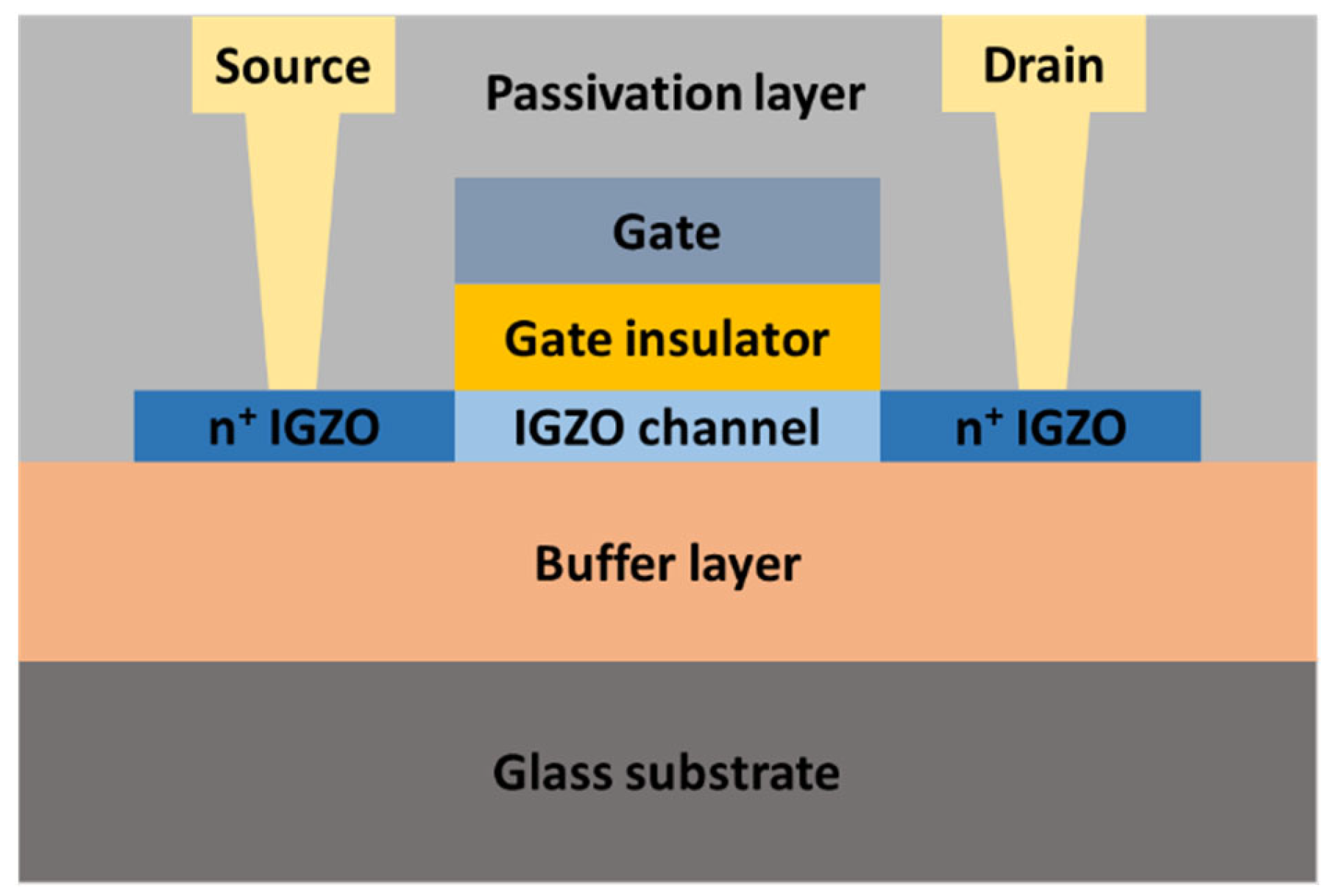
2. Experimental Section

SA-TG coplanar IGZO TFTs were fabricated as shown in Figure 1. First, a buffer layer (SiNX/SiO2 = 30/200 nm) was deposited by plasma-enhanced chemical vapor deposition (PECVD) on a glass substrate. A 40-nm-thick IGZO layer (In:Ga:Zn = 1:1:1 at.%) was deposited by RF sputtering on a buffer layer. A 120-nm-thick SiOX layer was deposited by PECVD as a gate insulator, followed by the sequential deposition of a gate metal (Ti/Mo = 30 nm/250 nm.). After the deposition and patterning of the gate electrode and gate insulator, 300-nm-thick SiOX and 200-nm thick SiNX were sequentially deposited as passivation layers by PECVD and patterned to form via holes. A metal layer (Ti/Al/Ti = 30/600/60 nm) was deposited and patterned as the source and drain electrodes. Finally, the devices were thermally annealed at 340 °C to achieve a stable and uniform electrical performance. The channel width (W) and length (L) were 3 and 5 μm, respectively. The electrical parameters of the representative device were as follows: field-effect mobility (μFE) of 8.1 cm2/Vs, threshold voltage (VTH) of 0.15 V, and SS of 0.19 V/dec. Here, μFE was determined using the maximum transconductance method, and VTH was defined as the gate-to-source voltage value (VGS) inducing a drain current (ID) of 1 nA at a VDS of 0.1 V. The energy distribution of the subgap DOS was extracted using the monochromatic photonic CV (MPCV) technique [18]. For MPCV characterization, a light source of 3 mW with a wavelength corresponding to the energy of 2.8 eV was used, and the CV curves were measured at 100 kHz. The ΔVTH decomposition was performed by the stress time-divided measurement technique [19]. The current–voltage and capacitance–voltage (C–V) characteristics of the TFTs were extracted using an Agilent 4156C semiconductor parameter analyzer (Agilent Technologies, Santa Clara, CA, USA) and a 4284A precision LCR meter (Agilent Technologies, Santa Clara, CA, USA), respectively. All measurements were performed under dark ambient conditions unless stated otherwise.

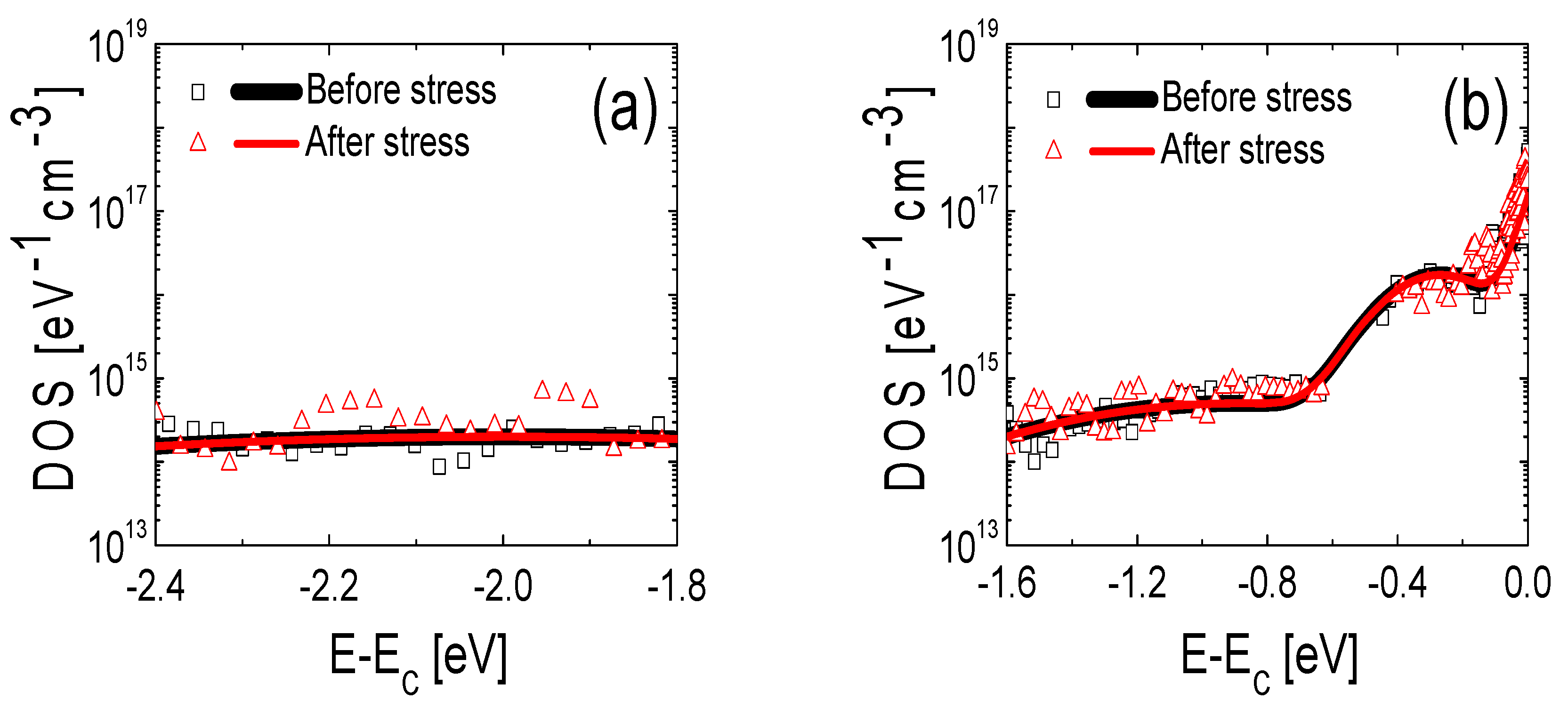
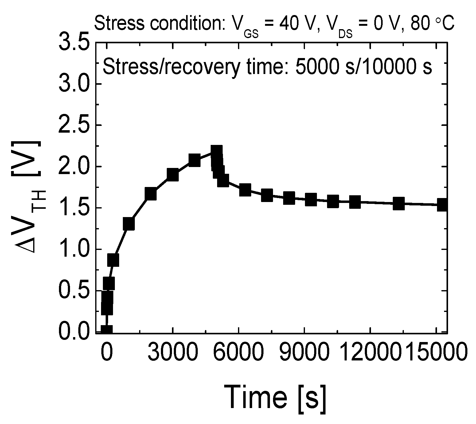
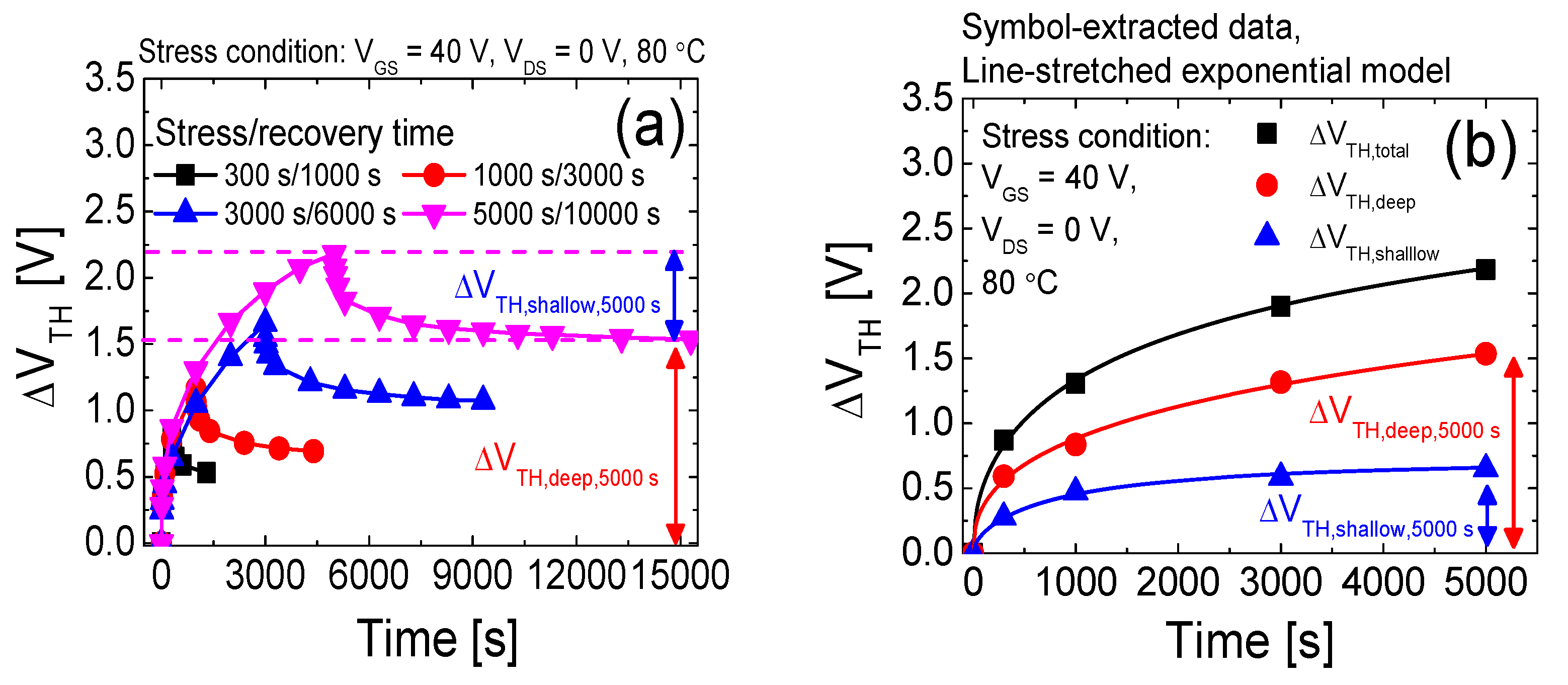
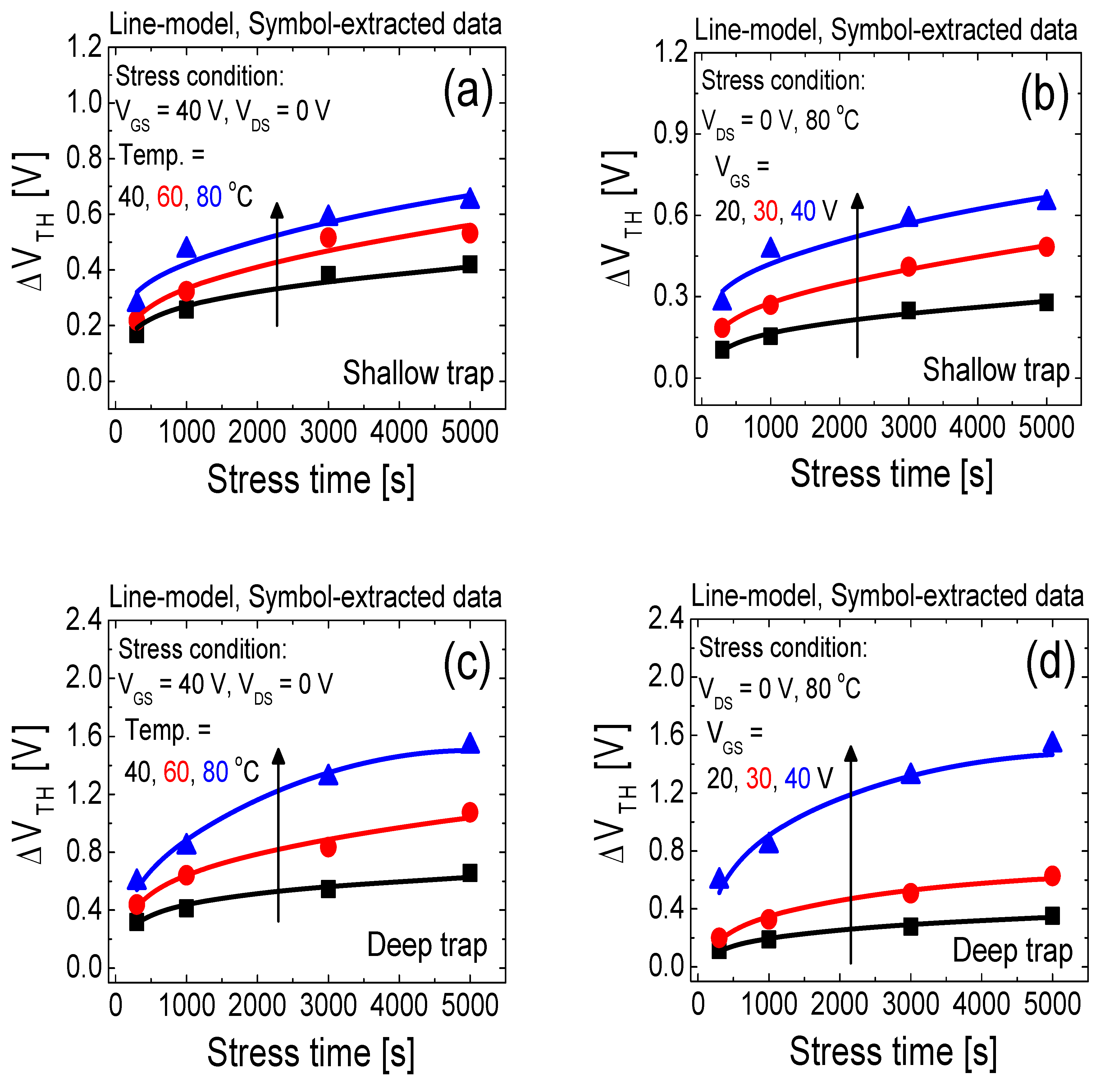
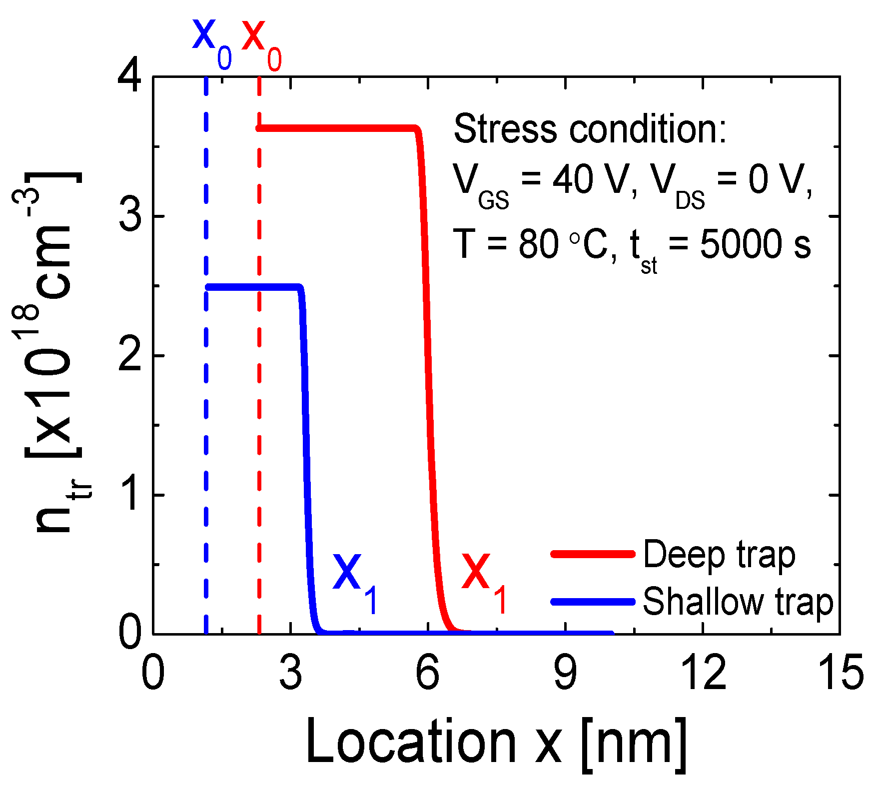
3. Results and Discussion

First, we examined the effects of PBTS on the subgap DOS in the fabricated SA-TG coplanar IGZO TFTs. Figure 2 shows the time evolution of the transfer curves for the fabricated SA-TG coplanar IGZO TFTs under a constant VGS and VDS of 40 V and 0 V, respectively, at 80 °C. The transfer curve shifted in the positive direction with an increase in the stress time; the SS value exhibited no significant change. Previous studies on well-passivated IGZO TFTs have reported that the PBTS-induced parallel shift of the transfer curves can primarily be attributed to the creation of acceptor-like states below the Fermi level in the IGZO channel layer or the electron injection from IGZO into the gate dielectric [20,21].
Therefore, the effects of PBTS on the subgap DOS in the channel layer must be examined before quantitatively analyzing the PBTS-induced trapped electron distribution within the gate dielectric in IGZO TFTs. Figure 3a,b demonstrate the energy distribution of the subgap DOS extracted using the MPCV technique before and after the application of the PBTS (VGS = 40 V, VDS = 0 V, 80 °C) for a stress time (tst) of 5000 s. The results presented in Figure 3 show that the difference between the energy distribution of the subgap DOS extracted from the TFT before and after PBTS was minimal, indicating that the electron injection from the channel (IGZO) to the gate dielectric (SiO2) in the fabricated SA-TG IGZO TFTs caused the PBTS-induced transfer curve shift observed in Figure 2.
Subsequently, we validated the assumption made in previous reports that electrons are trapped in the dielectric trap states only at a single energy level during PBTS in IGZO TFTs [10]. Figure 4 illustrates the time evolution of the threshold voltage shift (ΔVTH) during the stress (VGS = 40 V, VDS = 0 V, 80 °C, tst = 5000 s) and subsequent recovery (VGS = 0 V, VDS = 0 V, 80 °C, tst = 10,000 s) phases. The results reveal that the ΔVTH value decreased rapidly in the early stage of the recovery phase and was saturated at a certain value, implying that a part of trapped electrons were easily detrapped during this phase, but the remaining electrons were intact.
Figure 5a shows the time evolution of ΔVTH at different stress/recovery time pairs, and Figure 5b shows the time evolution of the PBTS-induced ΔVTH by both the recoverable and non-recoverable trapped electrons, obtained by applying the stress-time-divided measurement technique to Figure 5a. Figure 5b shows that the time evolution of both ΔVTH for the recoverable and non-recoverable trapped electrons were well-fitted by the stretched-exponential function. Generally, the stretched-exponential time dependence of ΔVTH is observed when electrons are trapped in the trap states at a single energy level [22,23]. The stretched-exponential equation for the ΔVTH(t) is defined as:
Δ V T H ( t ) = Δ V T H , 0 [ 1 exp ( ( t τ ) β ) ] ,
where ΔVTH,0 is the ΔVTH at infinite time, β is the stretched-exponential exponent, and τ = τ0 × exp(Ea/kT) represents the characteristic trapping time of carriers, and Ea is the average effective energy barrier that electrons in the IGZO TFT channel need to overcome before they can enter the insulator, and τ0 is the thermal prefactor for emission over the barrier. The lines in Figure 6a,b show that the recoverable trap component and the non-recoverable trap component was well fitted with the stretched exponential model functions. As shown in Figure 6c, the temperature dependence of the τ was confirmed, Ea was 0.29 eV for the recoverable trap and 0.78 eV for the non-recoverable trap.
Therefore, we can assume that the electrons were simultaneously trapped in the two dielectric trap states with different energy levels under PBTS in the fabricated IGZO TFTs. Hereafter, the gate dielectric trap where the trapped electrons can and cannot be easily detrapped during the recovery phase will be called as “shallow trap” and “deep trap”, respectively.
Finally, we extracted the PBTS-induced trapped electron distribution in the shallow and deep SiO2 gate dielectric traps in the fabricated SA-TG coplanar IGZO TFTs. Figure 7a presents the energy band diagram of the IGZO TFT under PBTS, where x represents the direction from the IGZO/SiO2 interface to SiO2. The energy level ET of the electron trap is defined by ΔEOT [eV], which indicates the energy difference between ET and the SiO2 conduction band minimum (EC, oxide). The Fermi energy level (EF) and ET cross at x0, which is extracted using the response time of the traps at the interface; the detailed methodology is provided in [24]. There were three different cases of trapped electrons in gate dielectrics under PBTS in IGZO TFTs. As depicted in Figure 7a, under a small VGS for a short tst, the electrons could not transfer to the position x0 and tunnel back easily to IGZO; as VGS and tst increased, the electrons tunneled deeper into the gate dielectric, and could not tunnel back easily to IGZO until they were trapped in ET below EF [10]. Further, as VGS and tst continued to increase, the trap states located near x0 were filled with electrons and thus could no longer capture them. The trapped electrons located below EF transferred to deeper positions by P–F conduction within the gate dielectric, as shown in Figure 7b [14,25].
Accordingly, the trapped electron distribution in the gate dielectric under PBTS can be expressed by the following equation [26,27]:
n t r t = G J n q x
where ntr represents the concentration of the filled trap states in SiO2 at time t and position x, Jn is the transport current density in SiO2, G is the generation rate of the trapped electrons, and q represents the electron charge.
The generation rate of the trapped electrons, G, is expressed based on the Shockley–Read–Hall recombination equation as follows [24,28]:
G = σ ( x ) v s n s ( N T n t r ) = σ 0 exp ( a x ) v s n s ( N T n t r )
where σ(x) = σ0 × exp(−ax) represents the location-dependent capture cross-section, σ0 is the capture cross-section at the semiconductor/gate dielectric interface, and a is the decay parameter, which depends on the tunneling effective mass of an electron and barrier height. In addition, vs represents the velocity at which the electrons move to the gate dielectric, and ns and NT are the electron density in the channel layer and trap density in the gate dielectric, respectively.
The PBTS-induced transport current density in the gate dielectric is described by the P–F conduction [13,14,26].
J n = n t r q Δ z r exp [ 1 ζ k T ( E O T β E 1 / 2 ) ]
where β = (q3/(πε0εSiO2))1/2. Δz is the mean distance between two adjacent SiO2 trap states, r is the characteristic P–F attempt frequency of the trapped electrons, T is the temperature, and ζ is the P–F factor. Additionally, k denotes the Boltzmann’s constant (8.62 × 10⁻⁵ eV), ε0 denotes the vacuum permittivity (8.854 × 10⁻¹⁴ F/cm), and εSiO2 denotes the relative permittivity of SiO2 (3.9). Because a significant portion of VGS falls on SiO2, the electric field in SiO2 (E) is expressed as EVGS/tox, where tox is the thickness of SiO2. By substituting equations (3) and (4) into (2) and solving the differential equation, we obtain:
n t r = N T { 1 exp [ exp ( a ( x x 1 ) ) ] }
x 1 = 1 a ln { K 2 a K 1 [ exp ( a K 1 t ) a ] }
K 1 = Δ z r exp [ 1 ζ k T s t ( E O T β E 1 / 2 ) ]
K 2 = S 0 υ s n s
Thus, Equations (5)–(8) represent the spatial and temporal trapped electron distributions in the gate dielectric. The PBTS-induced threshold voltage shift at time t, ΔVTH (t), can be expressed in terms of ntr and x as
Δ V T H ( t ) = x 0 x 1 q n t r ε 0 ε S i O 2 / ( t O X x ) d x = q n t r ε 0 ε S i O 2 ( x 1 x 0 ) ( t O X x 1 + x 0 2 )
where the parameters ntr, x0, x1, and EOT in Equations (5)–(9) are obtained as a function of the PBTS condition and tst [26]. The results presented in Figure 4, Figure 5 and Figure 6 show that the electrons were simultaneously trapped in the two dielectric trap states with different energy levels, called shallow and deep traps, under PBTS, in the fabricated IGZO TFTs. Therefore, we independently extracted the parameters ntr, x0, x1, and EOT for the electrons trapped in each gate dielectric trap under a specific PBTS condition. These parameters can be obtained from the separately extracted ΔVTH (t) values at that specific PBTS condition and T and VGS (or E)-dependence of each ΔVTH (t).
Figure 8a–d demonstrate the dependence of ΔVTH (t) on T and VGS for the electrons trapped in the shallow and deep traps under PBTS. By substituting the results in Figure 5b and Figure 8a–d into Equations (5)–(9), we could extract the ntr, x0, x1, and EOT parameters for each trap under specific PBTS conditions (in this study, VGS = 40 V, VDS = 0 V, 80 °C, tst = 5000 s). Figure 8 illustrates the extracted trapped electron distribution in the shallow and deep gate dielectric traps after the application of the PBTS (VGS = 40 V, VDS = 0 V, 80 °C) for 5000 s. Table 1 summarizes the ntr, x0, x1, and EOT values for the electrons in each type of trap. Although further study is necessary, the extracted EOT values for each gate dielectric trap suggest that the shallow and deep traps (Figure 9) possibly originated from the oxygen vacancy defect and E’ center defect in SiO2, respectively [29,30,31,32].

4. Conclusions

In this study, we quantitatively analyzed PBTS-induced electron trapping in the gate dielectric in SA-TG coplanar IGZO TFTs. First, we investigated the effects of PBTS on the subgap DOS in IGZO TFTs. Then, we examined the PBTS-induced ΔVTH values originating from electron trapping in shallow and deep gate dielectric traps. The data on the PBTS-induced trapped electrons in shallow and deep trap states was obtained from the analytical threshold voltage shift model based on trap-assisted tunneling and P–F effects. The extracted model parameters were ntr = 2.49 × 1018 cm−3, x0 = 1.2 nm, x1 = 3.3 nm, and EOT = 3.41 eV for the electrons trapped in shallow traps and ntr = 3.63 × 1018 cm−3, x0 = 2.3 nm, x1 = 5.9 nm, and EOT = 1.63 eV for the electrons trapped in deep traps. The results of this study are expected to be helpful in determining the physical origin of the gate dielectric traps, which degrade the PBTS stability in IGZO TFTs.

Author Contributions

Conceptualization, D.-H.K., H.-S.J., S.L., M.-H.K. and H.-I.K.; methodology, D.-H.K. and D.-H.L.; validation, M.-H.K., J.-H.L. and H.-I.K.; investigation, D.-H.K., H.-S.J., D.-H.L. and K.-H.B.; data curation, K.-H.B.; writing—original draft preparation, D.-H.K.; writing—review and editing, H.-I.K.; supervision, H.-I.K.; project administration, S.L. and J.-H.L. All authors have read and agreed to the published version of the manuscript.

Funding

This research was supported by Samsung Display Co., Ltd., and the National Research Foundation of Korea (NRF) grant funded by the Korea government (MSIT) (2019M3F3A1A03079821, 2020R1A2B5B01001765, 2021M3H2A1038042). This work was also supported by the Industry Technology R&D program (20006400), the Next-generation Display Expert Training Project for Innovation Process and Equipment, Materials Engineers (P0012453), and the HRD Program for Industrial Innovation (P0017011) funded by the Ministry of Trade, Industry and Energy (MOTIE) of the Republic of Korea.

Institutional Review Board Statement

Not applicable.

Informed Consent Statement

Not applicable.

Data Availability Statement

Not applicable.

Conflicts of Interest

The authors declare no conflict of interest.

References

  1. Kamiya, T.; Nomura, K.; Hosono, H. Present status of amorphous In–Ga–Zn–O thin-film transistors. Sci. Technol. Adv. Mater. 2010, 11, 044305. [Google Scholar] [CrossRef]
  2. Tripathi, A.K.; Smits, E.C.P.; Van Der Putten, J.B.P.H.; Van Neer, M.; Myny, K.; Nag, M.; Steudel, S.; Vicca, P.; O’Neill, K.; Van Veenendaal, E.; et al. Low-voltage gallium-indium-zinc-oxide thin film transistors based logic circuits on thin plastic foil: Building blocks for radio frequency identification application. Appl. Phys. Lett. 2011, 98, 162102. [Google Scholar] [CrossRef]
  3. Park, J.S.; Maeng, W.; Kim, H.; Park, J. Review of recent developments in amorphous oxide semiconductor thin-film transistor devices. Thin Solid Film. 2012, 520, 1679–1693. [Google Scholar] [CrossRef]
  4. Lin, C.-L.; Chang, W.-Y.; Hung, C.-C. Compensating pixel circuit driving AMOLED display with a-IGZO TFTs. IEEE Electron Dev. Lett. 2013, 34, 1166–1168. [Google Scholar] [CrossRef]
  5. Mo, Y.G.; Kim, M.; Kang, C.K.; Jeong, J.H.; Park, Y.S.; Choi, C.G.; Kim, H.D.; Kim, S.S. Amorphous-oxide TFT backplane for large-sized AMOLED TVs. J. Soc. Inf. Disp. 2012, 19, 16–20. [Google Scholar] [CrossRef]
  6. Liu, H.; Hussain, S.; Kang, J. Improvement in sensitivity of an indirect-type organic X-ray detector using an amorphous IGZO interfacial layer. J. Instrum. 2020, 15, P02002. [Google Scholar] [CrossRef]
  7. Hoshino, K.; Hong, D.; Chiang, H.Q.; Wager, J.F. Constant-voltage-bias stress testing of a-IGZO thin-film transistors. IEEE Trans. Electron Devices 2009, 56, 1365–1370. [Google Scholar] [CrossRef]
  8. Ji, K.H.; Kim, J.I.; Mo, Y.G.; Jeong, J.H.; Yang, S.; Hwang, C.S.; Park, S.H.K.; Ryu, M.K.; Lee, S.Y.; Jeong, J.K. Comparative Study on Light-Induced Bias Stress Instability of IGZO Transistors with SiNx and SiO2 Gate Dielectrics. IEEE Electron Device Lett. 2010, 31, 1404–1406. [Google Scholar] [CrossRef]
  9. Fomani, A.A.; Nathan, A. Metastability Mechanisms in Thin Film Transistors Quantitatively Resolved Using Post-Stress Relaxation of Threshold Voltage. J. Appl. Phys. 2011, 109, 084521–084526. [Google Scholar] [CrossRef]
  10. Xu, P.R.; Yao, R.H. Threshold-voltage shift model based on electron tunneling under positive gate bias stress for amorphous InGaZnO thin-film transistors. Displays 2018, 53, 14–17. [Google Scholar] [CrossRef]
  11. Oh, S.; Baeck, J.H.; Bae, J.U.; Park, K.-S.; Kang, I.B. Effect of interfacial excess oxygen on positive-bias temperature stress instability of self-aligned coplanar In-Ga-Zn-O thin-film transistors. Appl. Phys. Lett. 2016, 108, 141604. [Google Scholar] [CrossRef]
  12. Kim, D.H.; Choi, S.; Jang, J.; Kang, H.; Kim, D.M.; Choi, S.-J.; Kim, Y.-S.; Oh, S.; Baeck, J.H.; Bae, J.U.; et al. Experimental decomposition of the positive bias temperature stress-induced instability in self-aligned coplanar InGaZnO thin-film transistors and its modeling based on the multiple stretched-exponential function. J. Soc. Inf. Disp. 2017, 25, 98–107. [Google Scholar] [CrossRef]
  13. Harrell, W.R.; Frey, J. Observation of Poole-Frenkel Effect Saturation in SiO2 and Other Insulating Films. Thin Solid Films 1999, 352, 195–204. [Google Scholar] [CrossRef]
  14. Palit, S.; Alam, M.A. Theory of charging and charge transport in “intermediate” thickness dielectrics and its implications for characterization and reliability. J. Appl. Phys. 2012, 111, 054112. [Google Scholar] [CrossRef] [Green Version]
  15. Ma, Q.; Zhou, X.-Y.; Hsu, Y.-J.; Wu, Y.-C.; Zhang, S.-D. Excellent uniformity and reliability top-gate self-aligned IGZO TFTs with Cu electrode. SID Symp. Dig. Tech. Pap. 2020, 51, 184–186. [Google Scholar] [CrossRef]
  16. Song, Z.; Wang, G.; Chen, J.; Gu, P.; Liu, F.; Xie, D.; Liu, W.; Sun, H.; Song, Y.S.; Yan, L.; et al. 24.4: High Performance Top-gate Self-aligned Coplanar a-IGZO TFTs with Light Shielding Metal Design. SID Symp. Dig. Tech. Pap. 2018, 49, 259–262. [Google Scholar] [CrossRef]
  17. Hong, S.Y.; Kim, H.J.; Kim, D.H.; Jeong, H.Y.; Song, S.H.; Cho, I.T.; Noh, J.Y.; Yun, P.S.; Lee, S.W.; Park, K.S.; et al. Study on the Lateral Carrier Diffusion and Source-Drain. Series Resistance in Self-Aligned Top.-Gate Coplanar InGaZnO Thin-Film Transistors. Sci. Rep. 2019, 9, 6588. [Google Scholar] [CrossRef]
  18. Bae, H.; Choi, H.; Jun, S.; Jo, C.; Kim, Y.H.; Hwang, J.S.; Ahn, J.; Oh, S.; Bae, J.-U.; Choi, S.-J.; et al. Single-Scan Monochromatic Photonic Capacitance-Voltage Technique for Extraction of Subgap DOS Over the Bandgap in Amorphous Semiconductor TFTs. IEEE Electron Dev. Lett. 2013, 34, 1524–1526. [Google Scholar] [CrossRef]
  19. Choi, S.; Jang, J.; Kang, H.; Baeck, J.H.; Bae, J.U.; Park, K.-S.; Yoon, S.Y.; Kang, I.B.; Kim, D.M.; Choi, S.-J.; et al. Systematic decomposition of the positive bias stress instability in self-aligned coplanar In-Ga-Zn-O thin-film transistors. IEEE Electron Dev. Lett. 2017, 38, 580–583. [Google Scholar] [CrossRef]
  20. Lee, H.-W.; Choi, H.-S.; Cho, W.-J. Improving Charge Trapping/Detrapping Characteristics of Amorphous In-Ga-ZnO Thin-Film-Transistors Using Microwave Irradiation. J. Nanosci. Nanotechnol. 2019, 19, 6164–6169. [Google Scholar] [CrossRef]
  21. Hsieh, H.H.; Kamiya, T.; Nomura, K.; Hosono, H.; Wu, C.C. Modeling of amorphous InGaZnO4 thin film transistors and their subgap density of states. Appl. Phys. Lett. 2008, 92, 10–13. [Google Scholar] [CrossRef]
  22. Yoon, S.J.; Seong, N.J.; Choi, K.J.; Shin, W.C.; Yoon, S.M. Investigations on the bias temperature stabilities of oxide thin film transistors using In–Ga–Zn–O channels prepared by atomic layer deposition. RSC Adv. 2018, 8, 25014–25020. [Google Scholar] [CrossRef] [Green Version]
  23. Chen, T.-C.; Chang, T.-C.; Tsai, C.-T.; Hsieh, T.-Y.; Chen, S.-C.; Lin, C.-S.; Hung, M.-C.; Tu, C.-H.; Chang, T.-C.; Chen, P.-L. Behaviors of InGaZnO thin film transistor under illuminated positive gate-bias stress. Appl. Phys. Lett. 2010, 97, 112104. [Google Scholar] [CrossRef]
  24. Koelmans, H.; De Graaff, H.C. Drift phenomena in CdSe thin film FET’s. Solid State Electron. 1967, 10, 997–1000. [Google Scholar] [CrossRef]
  25. Jonscher, A.K. Energy losses in hopping conduction at high electric fields. J. Phys. C 1971, 4, 1331–1340. [Google Scholar] [CrossRef]
  26. Wang, L.L.; Liu, T.C.; Cai, Y.; Zhang, S. Thin-film transistor Vth shift model based on kinetics of electron transfer in gate dielectric. IEEE Trans. Electron Devices 2014, 61, 1436–1443. [Google Scholar] [CrossRef]
  27. Wang, L.L.; He, H.; Liu, X.; Deng, W.; Zhang, S. Charge Trapping Model for Temporal Threshold Voltage Shift in a-IGZO TFTs Considering Variations of Carrier Density in Channel and Electric Field in Gate Insulator. IEEE Trans. Electron. Devices 2015, 62, 2219–2225. [Google Scholar] [CrossRef]
  28. Fomani, A.A. Threshold Voltage Instability and Relaxation in Hydrogenated Amorphous Silicon Thin Film Transistors. Master’s Thesis, Waterloo University, Waterloo, ON, Canada, 2005. [Google Scholar]
  29. Eoin, P.; Robertson, J. Theory of defects in vitreous silicon dioxide. Phys. Rev. B 1983, 27, 3780–3795. [Google Scholar]
  30. Warren, W.L.; Lenahan, P.M.; Robinson, B.; Stathis, J.H. Neutral E’ centers in microwave downstream plasma-enhanced chemical-vapor-deposited silicon dioxide. Appl. Phys. Lett. 1988, 53, 482. [Google Scholar] [CrossRef]
  31. Pantelides, S.T.; Lu, Z.-Y.; Nicklaw, C.; Bakos, T.; Rashkeev, S.N.; Fleetwood, D.M.; Schrimpfc, R.D. The E′ center and oxygen vacancies in SiO2. J. Non-Cryst. Solids 2008, 354, 217–223. [Google Scholar] [CrossRef]
  32. El-Sayed, A.-M.; Watkins, M.B.; Shluger, A.L.; Afanas’ev, V.V. Identification of intrinsic electron trapping sites in bulk amorphous silica from ab initio calculations. Microelectron. Eng. 2013, 109, 68–71. [Google Scholar] [CrossRef] [Green Version]
Figure 1. Structure of the fabricated SA-TG coplanar IGZO TFT.
Coatings 11 01192 g001
Figure 2. Time evolution of the transfer curves for the fabricated SA-TG coplanar IGZO TFT under a constant VGS of 40 V and VDS of 0 V at 80 °C.
Coatings 11 01192 g002
Figure 3. Energy distribution of subgap DOS in IGZO near (a) the valence band maximum (EV) and (b) the conduction band minimum (EC) obtained using MPCV before and after the application of the PBTS (VGS = 40 V, VDS = 0 V, 80 °C) for 5000 s. Dotted symbols and lines denote the experimental data and fitting curves, respectively.
Coatings 11 01192 g003
Figure 4. Time evolution of ΔVTH during the stress (VGS = 40 V, VDS = 0 V, 80 °C, tst = 5000 s) and subsequent recovery (VGS = 0 V, VDS = 0 V, 80 °C, tst = 10,000 s) phases.
Coatings 11 01192 g004
Figure 5. (a) Time evolution of ΔVTH at different stress/recovery time pairs. (b) Time evolution of the PBTS-induced ΔVTHs for the recoverable and non-recoverable trapped electrons obtained by applying the stress-time-divided measurement technique to (a).
Coatings 11 01192 g005
Figure 6. (a) Dependence of ΔVTH (t) on stress temperature for the electrons trapped in the shallow trap under PBTS (VGS = 40 V, VDS = 0 V, tst = 5000 s). (b) Dependence of ΔVTH (t) on stress temperature for the electrons trapped in the deep trap under PBTS. (c) Characteristic time constant as a function of the PBTS temperature to extract the effective energy barrier (activation energy), for each trap.
Coatings 11 01192 g006
Figure 7. (a) Energy band diagram for the IGZO TFT under PBTS, in which x represents the direction from the IGZO/SiO2 interface to SiO2. (b) PBTS-induced electron tunneling from IGZO to SiO2 and PF conduction of trapped electrons in SiO2.
Coatings 11 01192 g007
Figure 8. Dependencies of ΔVTH (t) on (a) T and (b) VGS for the electrons trapped in the shallow trap under PBTS (VGS = 40 V, VDS = 0 V, 80 °C). Dependencies of ΔVTH (t) on (c) T and (d) VGS for the electrons trapped in the deep trap under PBTS (VGS = 40 V, VDS = 0 V, 80 °C).
Coatings 11 01192 g008
Figure 9. Extracted trapped electron distribution in the shallow and deep gate dielectric traps after the application of the PBTS (VGS = 40 V, VDS = 0 V, 80 °C) for 5000 s in the fabricated SA-TG coplanar IGZO TFT.
Coatings 11 01192 g009
Table 1. Extracted values of ntr, x0, x1, and EOT for electrons trapped in shallow and deep traps under PBTS (VGS = 40 V, VDS = 0 V, 80 °C) in the fabricated IGZO TFT.
ParameterShallow TrapDeep Trap
ntr (cm−3)2.49 × 10183.63 × 1018
EOT (eV)3.411.63
x0 (nm)1.22.3
x1 (nm)3.35.9
Publisher’s Note: MDPI stays neutral with regard to jurisdictional claims in published maps and institutional affiliations.

