Abstract
Over the past few years, thermoelectrics have gained interest with regard to thermoelectricity interconversion. The improvement in the efficiency of the thermoelectric material at an ambient temperature is the main problem of research. In this work, silicon–germanium (SiGe) thin films, owing to superior properties such as nontoxicity, high stability, and their integrability with silicon technologies, were studied for thermoelectric applications. P-type SiGe thin films were deposited on quartz substrates by DC/RF magnetron sputtering and annealed at three different temperatures for 1 hour. Significant enhancement in the Seebeck coefficient was achieved for the sample annealed at 670 °C. A high power factor of 4.1 μWcm−1K−2 was obtained at room temperature.
1. Introduction
Over the last few years, thermoelectric materials have been compelling ample consideration among the scientific community for use in generating electricity from heat, thus establishing a sustainable and clean energy source [1]. Thermoelectrics based on power generation is paving the way towards new mute technology in electric appliances, as these materials are foreseen to replace the conventional materials. Being a stationary setup, it also aids to the sustainability of devices with a higher output power compared to conventional designs. The concept of self-powered devices, utilizing the exchange of body heat into electrical power through a thermoelectric (TE) power generator, is implemented for wearable, portable electronic devices, such as medical sensors, mobiles, and smart watches [2,3]. TE generators are also used as a heat recovery tool in the automotive industry and as power generators in space exploration missions [4]. Nevertheless, a primary hurdle in implementing the application of these devices still exists due to the poor efficiency of thermoelectric materials compared to conventional heat and thermodynamical systems and poor heat exchanger system design.
There are three physical phenomena that explain the underlying mechanism of the production of electricity through heat energy, named the Seebeck effect, the Peltier effect, and the Thomson effect. All of these are different manifestations of the same thermodynamical effect in which differences in temperature produce differences in voltages. The Seebeck effect is the generation of potential gradient due to a difference in temperature between two dissimilar semiconductors, while the Peltier effect deals with the presence of heat at the electrified junction of two dissimilar semiconductors. The Thomson effect illustrates the exchangeable phenomenon of heating or cooling in a homogeneous semiconductor material subjected to an electric current flow and temperature gradient [5]. Electrical conductivity (σ) and thermal conductivity (κ) are significant factors for an energy conversion assessment of these particular materials at a given temperature (T), along with the thermoelectric power (S) and the power factor (PF) to correlate all of them to define a dimensionless quantity known as the figure of merit (ZT), represented by following equation:
The right side power factor (PF) is explicitly introduced for thin films, whose thermal conductivity (κ) estimations are difficult to measure. As it can be deduced from Equation (1), in order to attain the ZT exceeding a unit value, it is imperative to scale down the values of electrical resistivity, as well as thermal conductivity in parallel, to raise thermoelectric power. This is a guiding aim for all thermoelectric materials to achieve and to be considered as thermoharvesters in comparison to typical electric power sources. Nanoscale heterostructure-based devices are anticipated to have a potential boost in their figure of merit, in line with the theoretically reported values. In addition, the thermoelectric efficiency of tellurium-based materials has also demonstrated the highest peaks in the literature through these nano-engineering techniques [6]. The simplistic design structure, low synthetic costs, and planar integration of thin film proves as a potential design structure for device applications. Through this nanostructuring technique, a large area can be treated. Thin films are a step forward towards the commercial application of thermoelectric devices, as both p and n-type material can be availed [7].
The alloying effect of silicon and germanium materials has been established exceptionally in the field of thermoelectrics at higher operational temperatures [8,9,10]. Beyond this, the optimization to achieve higher thermoelectric efficiency is experimentally proven through the Si-Ge nanocomposite approach in comparison to their bulk counterpart. Metal/semiconductor nanocomposites are ideal to achieve a high power factor, as reported in the case of Au-doped SiGe thin films [9,11]. Even the output power of heavily doped metal/semiconductor compositions is far more reaching than that of the heteroepitaxially grown supper lattices of p-type and n-type tellurides and titanates composites [1,6,12]. In this work, the thermoelectric properties of polycrystalline p-type SiGe thin films were studied. The SiGe thin films were deposited on quartz substrates using magnetron sputtering. The effect of the annealing temperature on the crystallization and transport properties of the SiGe alloy films was investigated based on the hypothesis: the crystallinity is crucial for exploiting high electrical conductivity, contributing to an increase in the thermoelectric power factor. Enhancement in the thermoelectric performance of these films was observed and compared to previously reported results. In particular, the high value of the Seebeck coefficient was obtained.
2. Experimental Details
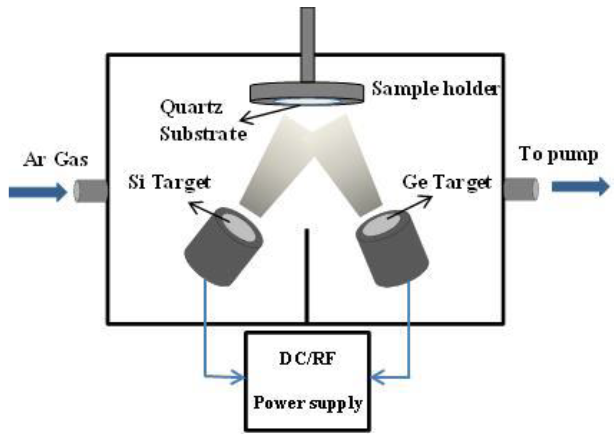
The p-type SiGe films were deposited on a pre-cleaned quartz substrates using single-crystal heavily doped p-type Si (99.9999% pure and ρ = 0.005–0.020 Ω.cm), and single-crystal n-type Ge (99.999% pure and ρ > 0.1 Ω.cm) targets by DC/RF Magnetron Sputter-NanoPVD (Model: S10A, Moorfield, UK). Figure 1 shows the schematic diagram of the deposition process of the SiGe films by co-sputtering of Si and Ge. The chamber was evacuated to the base pressure of 4.73 × 10⁻⁷ mbar. The highly doped p-type silicon (Si) target was used as a DC source and the low doped n-type germanium (Ge) was used as the RF source. Argon (Ar) was used as the sputter gas with a flow rate of 9.6 sccm. The deposition was carried out at room temperature with a rotating substrate (rotation speed of 2 rpm). Pre-sputtering was carried out to clean the surface of the targets with closed shutters to avoid any contamination of the deposited film. The deposition time was 4 h. Details of the growth parameters are given in Table 1.
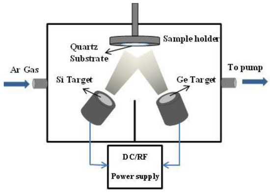
Figure 1.
Schematic diagram of co-sputtering by physical vapor deposition (nano-PVD).

Table 1.
Parameters for deposition of SiGe thin film.
The thickness of the SiGe film was estimated by a cross-sectional scanning electron microscopy (SEM) image of the deposited film and was found to be ~950 nm with a deposition rate of 3.96 nm·min−1. The deposited films were annealed at 670, 800, and 900 °C, under a nitrogen flow of 2.6 NL/min for 1 h in a tube furnace (Model: small blue tube furnace, temperature range: 25–1200 °C). The crystallographic parameters of the SiGe films were measured using thin film X-ray diffraction (Model: AXS D8 Discover, Bruker, Billerica, MA, USA) with a CuKα radiation source of 0.154 nm wavelength, a step size of 0.01°, and a scan speed 0.1 s per step. The surface morphology and composition of the deposited films were observed by a scanning electron microscope SEM/EDS (Model: IT-300, JEOL, Tokyo, Japan), with an accelerating voltage of 20 kV. A Raman spectrometer (Model: MN STEX-PRI 100, Photon Systems, Bruker, Billerica, MA, USA) with a laser wavelength of 632.8 nm was used to obtain the Raman spectra of the SiGe thin films. The in-plane Seebeck coefficient (S) measurements were performed at room temperature by a home-made setup. A temperature gradient was developed between the two opposite ends of the sample by heating one end using a heater and placing the other end on a cooler. The temperature difference ∆T between the two ends of the sample was measured using two thermocouples placed at both ends, and the Seebeck voltage ∆V was measured using the two probes across the ends. Figure 2 shows the schematic diagram of the Seebeck measurement setup. The Seebeck voltage was recorded at the temperature difference ∆T (°C) of 2, 4, 6, 8, 10 and 12, and the value of the Seebeck coefficient S was obtained from the slope of the ∆T-∆V curve, as S is the ratio between the Seebeck voltage and the negative of the temperature difference [13]. The electrical conductivity (σ) measurements were carried out by a four-probe setup (Model: KM3-AR, Jandel, Leighton Buzzard, UK). All the characterizations were performed at room temperature.
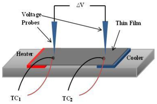
Figure 2.
Schematic diagram of homemade setup for Seebeck coefficient measurement.
3. Results and Discussion
3.1. XRD
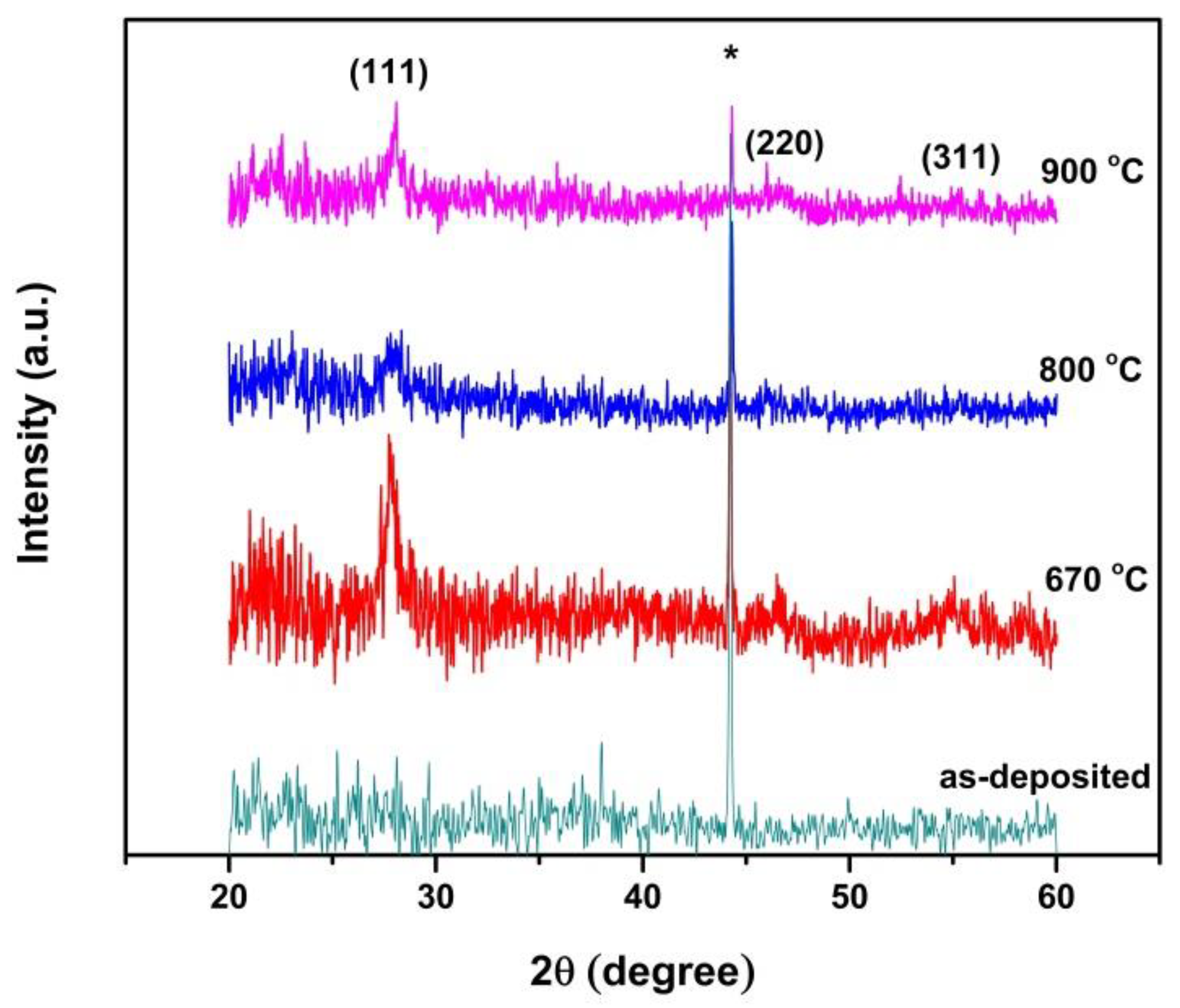
The XRD patterns of the as-deposited, 670, 800, and 900 °C annealed thin films of the SiGe alloy over the quartz substrates are shown in Figure 3. The XRD pattern of the as-deposited SiGe film demonstrated an amorphous nature. However, a peak marked as (*) belonged to an aluminum sample stage (JCPDS#: 00-004-0787). The XRD patterns from the samples annealed at 670, 800, and 900 °C showed that the SiGe alloy peaks at ~28°, 46°, and 55.3° related to (1 1 1), (2 2 0) and (3 1 1) planes of the SiGe alloy, respectively. The (1 1 1) peak was of a relatively high intensity and the presence of higher order peaks showed that the annealed SiGe films were crystalline in nature. A decrease in the intensity of all the peaks was observed from measurement to measurement, which occurred due to the apparatus artifact. The relative increase in the intensity of the (1 1 1) peak with an increasing annealing temperature showed improvement in the crystallinity of the SiGe thin films. The crystallite sizes of the annealed films were estimated with respect to the dominant peak (1 1 1) using Scherrer`s formula, given by the following Equation (2):
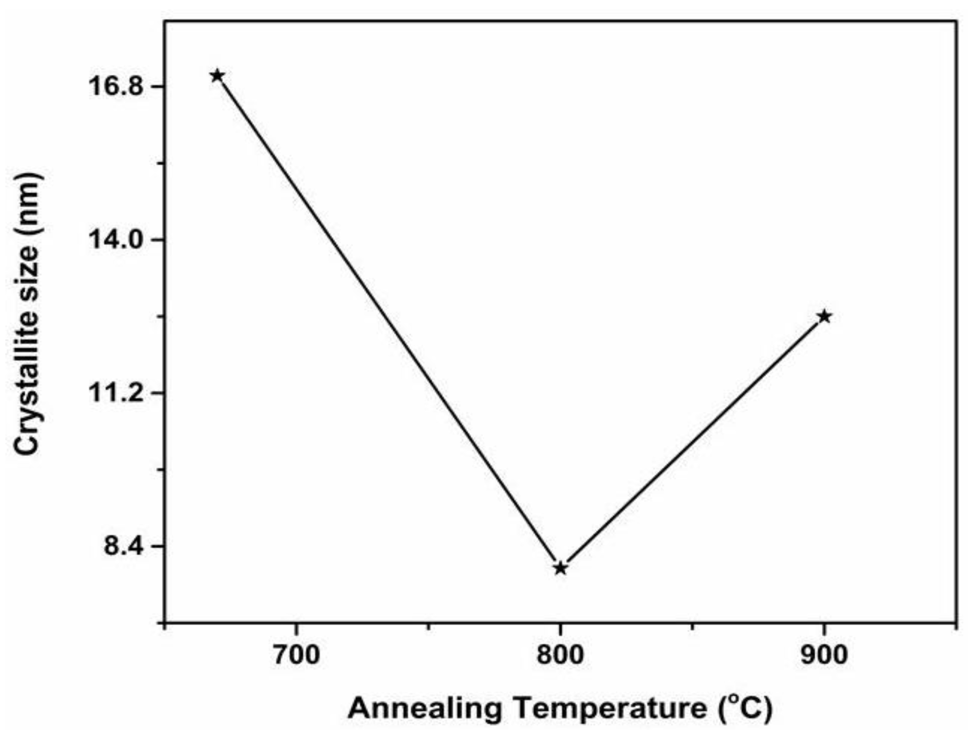
where β is the full width at half the maximum FWHM of the peak, K is the shape factor ~0.96, λ is the wavelength of the X-rays, and θ is the Bragg’s angle. The change in the crystallite size of the annealed films with an increase in the annealing temperature is displayed in Figure 4. It was observed that from 670 to 800 °C, the crystallite size changed from 17 nm to 8 nm; then, at 900 °C, it increased again to 12 nm. The reason for the decrease in the crystallite size at 800 °C may be associated with structural changes in the film, as explained earlier in the XRD pattern. The broadness of the (1 1 1) peak at 800 °C (in Figure 3) strengthens our assumption.
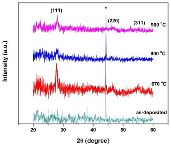
Figure 3.
XRD patterns of SiGe/quartz thin films. The peak marked as (*) belongs to sample stage.

Figure 4.
Influence of annealing temperature on crystalline size of SiGe thin films.
3.2. Raman Spectroscopy
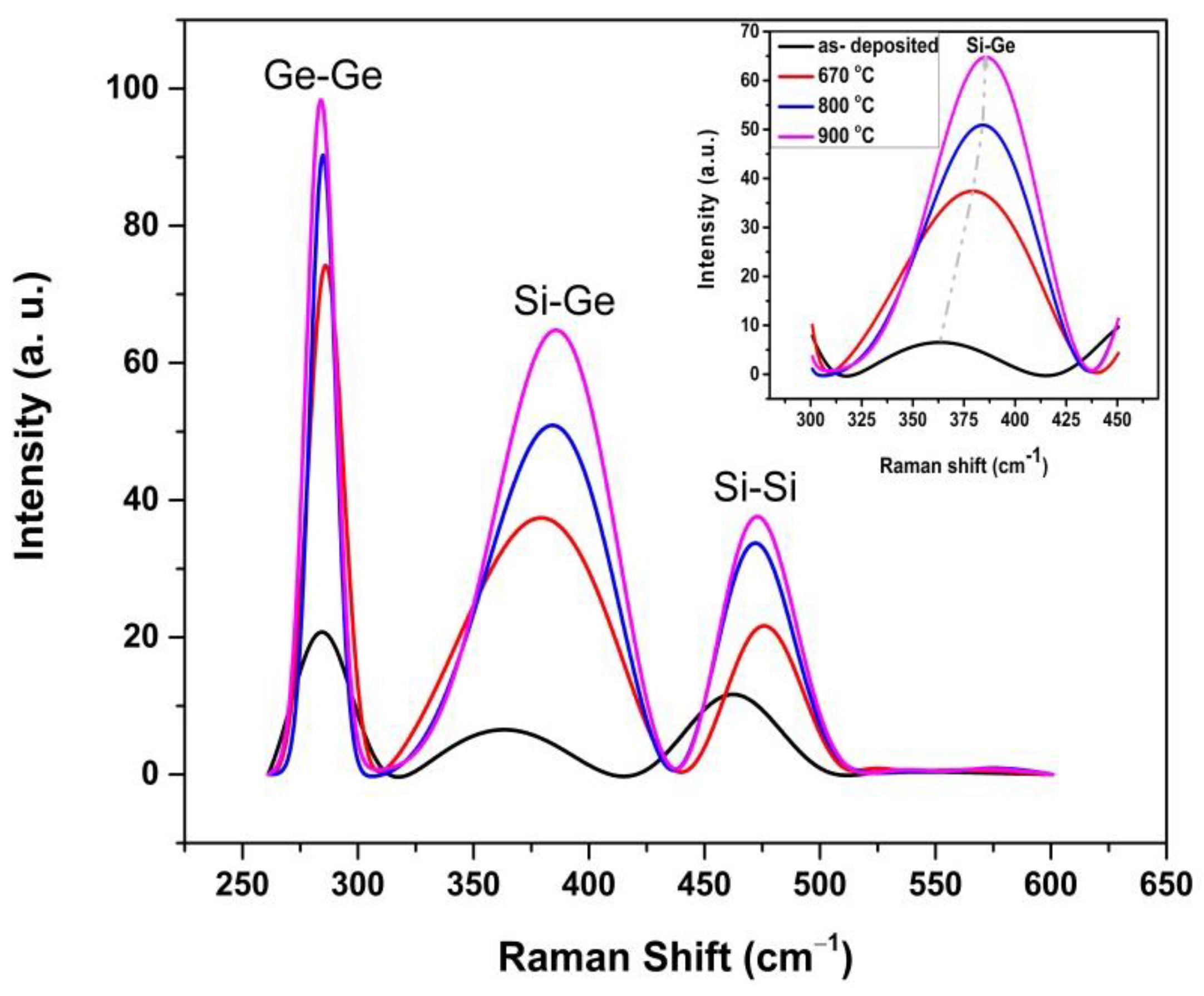
For more insight into the effect of the annealing temperature on the alloying process, Raman spectroscopy was performed. Figure 5 shows the Raman spectra of p-type SiGe thin films annealed at different temperatures. For reference, the Raman scan of the as-deposited SiGe film was also included. The scan from the as-deposited sample showed peaks near 284, 363, and 462 cm−1, related to the Ge-Ge, Si-Ge, and Si-Si TO (transverse optic) vibrational modes, respectively [14,15]. The peak from the Si-Ge vibrational mode confirmed the formation of the SiGe alloy. Furthermore, the Raman scans from the annealed samples revealed a blue-shift of the Si-Si and Si-Ge peaks to a higher wavenumber and a red-shift of the Ge-Ge peak to a lower wavenumber. There are two possible causes for these shifts in peaks: (i) changes in Si and Ge concentration in the SiGe thin films; and (ii) strain relaxation at higher annealing temperatures [16,17]. The shift in the Si-Ge peak with an annealing temperature is shown by the inset in Figure 4.

Figure 5.
Raman scans of as-deposited and 670, 800, and 900 °C annealed SiGe/quartz thin films. The inset displays shift in Si-Ge peak with annealing temperature.
The strain ε and the Ge content x in the SiGe thin films were calculated by the following pair of equations [18]:
As obtained, x and ε are depicted in Table 2. These values exhibited the increase in the Ge concentration and ε with an increasing annealing temperature in the SiGe thin films. These findings are understandable as the causes of the shifts in the Raman peaks.
Table 2.
Germanium content and strain in as-deposited and annealed SiGe thin films.
3.3. SEM
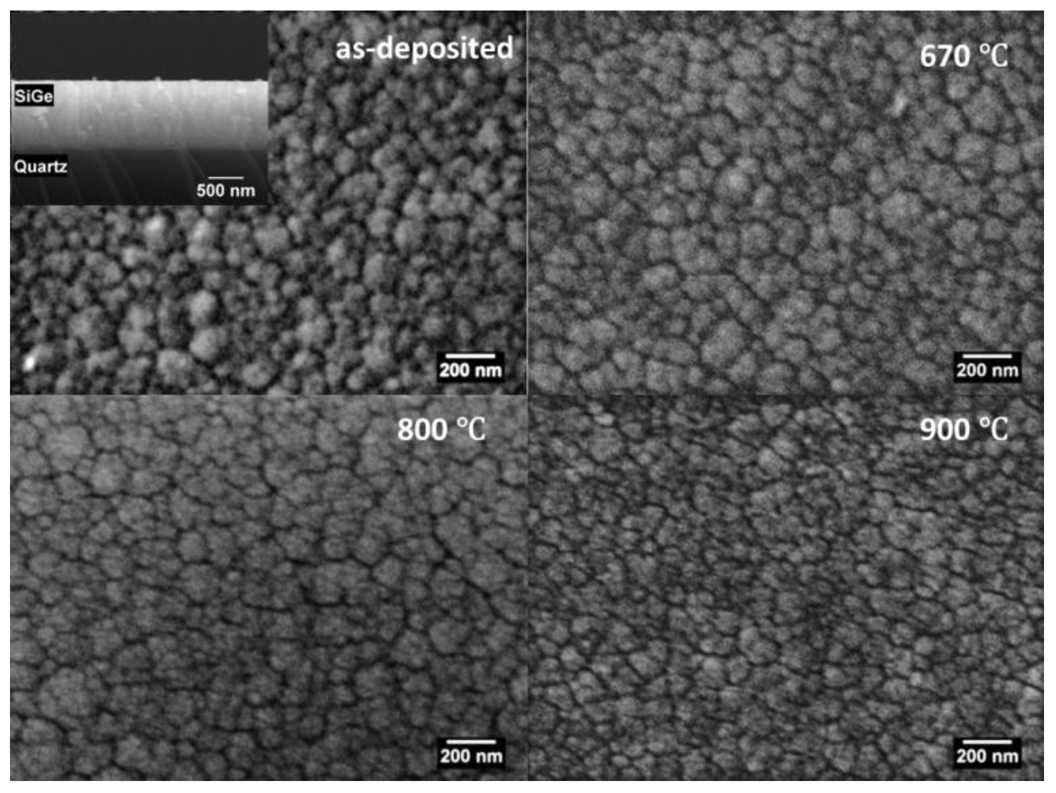
The SEM images of the as-deposited and annealed p-type SiGe thin films are presented in Figure 6; the average grain size in each image was estimated with the help of ImageJ (ver. 1.52a) software. There was small increase in the grain size of the thin films annealed at 670 °C. However, at a higher annealing temperature, the decrease in grain size occurred, as depicted in Table 3. The general trend of the grain size is consistent with the XRD measurements.

Figure 6.
The SEM images of as-deposited, 670, 800, and 900 °C annealed p-type SiGe/ quartz thin films. The inset shows cross-sectional view of as-deposited thin film.
Table 3.
Average grain size of as-deposited and annealed SiGe thin films.
3.4. Thermoelectric Properties
Figure 7 shows the temperature difference dependent on the Seebeck voltage (∆V) of 670, 800, and 900 °C annealed p-type SiGe/quartz thin films for 1 h under a nitrogen flow. The data corresponding to the as-deposited SiGe thin film were also included for reference. The measurements carried out at room temperature show that the Seebeck voltage increased with an increase in temperature difference. The value of the Seebeck voltage for the 670 °C annealed sample was greater than the as-deposited SiGe thin film. The values of ∆V decreased with a further increase in the annealing temperature. The sign of the Seebeck voltage was positive, indicating that the thin films were p-type. It is worthwhile to mention here that the source of the p-type SiGe thin film was a highly doped Si target, used in the deposition chamber.
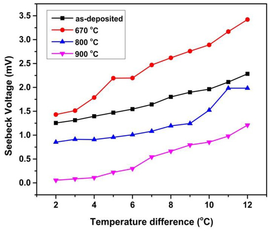
Figure 7.
Graph displaying Seebeck voltage and temperature difference of as-deposited and annealed p-type SiGe thin films.
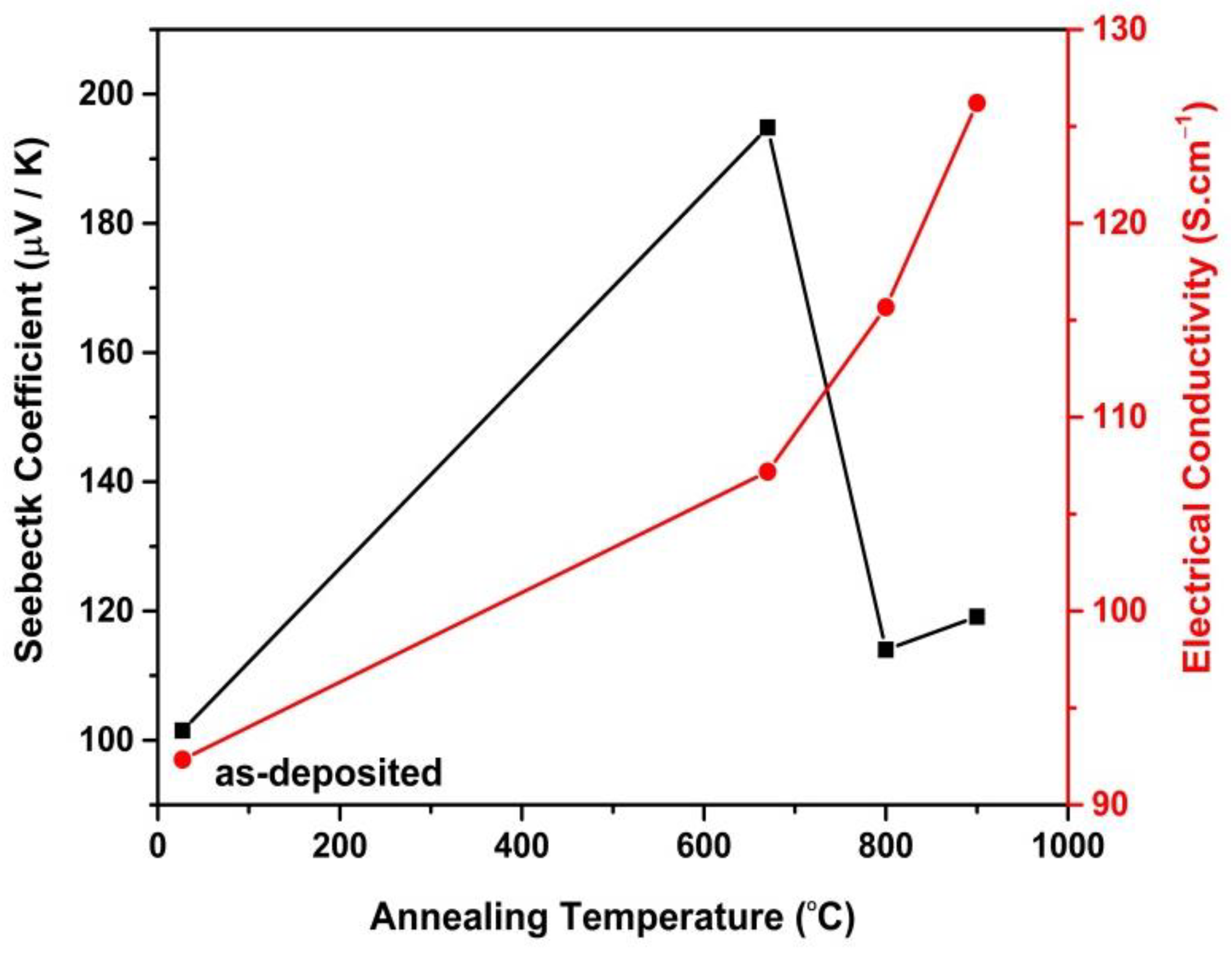
The variation in the value of the Seebeck coefficient and the electrical conductivity, measured at room temperature with an annealing temperature, is presented in Figure 8. The value of S is highest for the 670 °C annealed p-type SiGe thin film and is equal to 195 μVK−1, which is greater than the typical bulk p-type SiGe alloy (121 μVK−1) [19]. For the 800 °C annealed sample, S decreased to ~114 μVK−1 and slightly increased for the 900 °C annealed sample, in accordance with the Seebeck voltage. This behavior can be attributed to the increase in carrier concentration with a change in the Ge content in the SiGe thin films at a higher annealing temperature, as S has an inverse relation with the carrier concentration [20,21]. In other words, at 670 °C, the structure of the SiGe thin film transformed from amorphous to crystalline, which resulted in the enhancement of the Seebeck coefficient. With a further increase in the annealing temperature, the increase in the Ge content caused an increase in carrier concentration, which decreased the Seebeck coefficient value. The Seebeck coefficient value of all the annealed SiGe thin films was greater than the as-deposited samples. The sign of S was positive, indicating that the dominant charge carriers for the deposited thin films were holes.
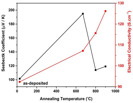
Figure 8.
Effect of annealing temperature on Seebeck coefficient (left) and electrical conductivity (right) of SiGe thin films.
The electrical conductivity of all the annealed SiGe thin-films was higher than the electrical conductivity of the as-deposited thin film (92.3 S·cm−1) and increased with the increasing annealing temperature up to 126 S·cm−1 for the 900 °C annealed sample. The enhancement in the electrical conductivity is accredited to an increase in the carrier concentration caused by annealing the SiGe thin films at a high temperature, as conductivity increases with increasing the carrier concentration.
Figure 9 shows the power factor (S2σ) of the as-deposited and annealed films at 670, 800, and 900 °C SiGe thin films. The power factor (PF) value reached its maximum for the SiGe film annealed at 670 °C, and for higher annealing temperatures, the thin films had a low PF value. This decrease in the PF value was attributed to the low Seebeck coefficient at 800 and 900 °C. The results show that the optimal annealing temperature for the p-type SiGe alloy thin films was around 670 °C. The maximum value of the PF attained for our samples was equal to 4.1 μWcm−1K−2, which is greater than that previously reported other p-type thermoelectric thin films at room temperatures. For instance, Lal et al. reported p-type BiSbTe thin films with a PF of 2.4 μWcm−1K−2, le Febvrier et al. reported p-type Cr0.96Al0.04N1.17 thin film with a PF of 0.5 μWcm−1K−2, and C. Yang et al. reported p-type CuI thin films with a PF of 3.75 μWcm−1K−2 [19,22,23].
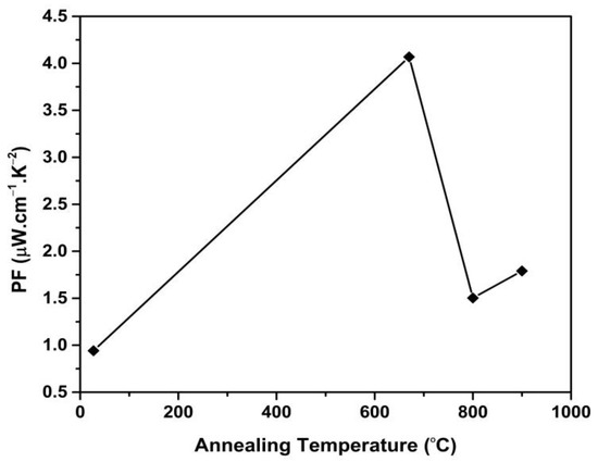
Figure 9.
Annealing temperature dependent power factor (PF) of SiGe thin films.
4. Conclusions
In this work, p-type SiGe thin films were deposited on quartz substrate by DC/RF magnetron sputtering. The deposited SiGe films that annealed at 670, 800, and 900 °C were polycrystalline with an average grain size of 35–120 nm. An increase in the Ge content was observed in the thin films with an increasing annealing temperature by the Raman analysis. The conductivity of the deposited thin films enhanced with an increase in the annealing temperature. The maximum Seebeck coefficient obtained was equal to 195 μVK−1, with a maximum power factor of 4.1 μWcm−1K−2 for the same sample. The obtained power factor value was high compared to that of other reported p-type materials [19,22,23]. The results showed that the optimal annealing temperature for the sputtered SiGe thin films was around 670 °C.
Author Contributions
Conceptualization, methodology, investigation, writing original draft: K.F.; visualization, data curation: H.N.; investigation, formal analysis: A.A.; project administration, resources: E.M.; supervision, writing—review and editing: M.A. All authors have read and agreed to the published version of the manuscript.
Funding
This research received no external funding.
Institutional Review Board Statement
Not applicable.
Informed Consent Statement
Not applicable.
Data Availability Statement
Data are contained within the article.
Acknowledgments
The authors highly acknowledge the financial support from IRSIP HEC Pakistan for working at University of Oslo, Norway.
Conflicts of Interest
The authors declare no conflict of interest.
References
- Takiguchi, H.; Matoba, A.; Sasaki, K.; Okamoto, Y.; Miyazaki, H.; Morimoto, J. Structural properties of heavily B-doped SiGe thin films for high thermoelectric power. Mater. Trans. 2010, 51, 878–881. [Google Scholar] [CrossRef] [Green Version]
- Peng, Y.; Miao, L.; Gao, J.; Liu, C.; Kurosawa, M.; Nakatsuka, O.; Zaima, S. Realizing high thermoelectric performance at ambient temperature by ternary alloying in polycrystalline Si1−x−yGexSny thin films with boron ion implantation. Sci. Rep. 2019, 9, 14342. [Google Scholar] [CrossRef] [PubMed]
- Alam, H.; Ramakrishna, S. A review on the enhancement of figure of merit from bulk to nano-thermoelectric materials. Nano Energy 2013, 2, 190–212. [Google Scholar] [CrossRef]
- Rowe, D.M. Thermoelectric waste heat recovery as a renewable energy source. Int. J. Innov. Energy Syst. Power 2006, 1, 13–23. [Google Scholar]
- Borup, K.A.; de Boor, J.; Wang, H.; Drymiotis, F.; Gascoin, F.; Shi, X.; Chen, L.; Fedorov, M.I.; Müller, E.; Iversen, B.B.; et al. Measuring thermoelectric transport properties of materials. Energy Environ. Sci. 2015, 8, 423–435. [Google Scholar] [CrossRef] [Green Version]
- Venkatasubramanian, R.; Siivola, E.; Colpitts, T.; O’Quinn, B. Thin-Film Thermoelectric Devices with High Room-Temperature Figures of Merit. Nature 2001, 413, 597–602. [Google Scholar] [CrossRef] [PubMed]
- Xie, K.; Mork, K.; Kortshagen, U.; Gupta, M.C. High temperature thermoelectric properties of laser sintered thin films of phosphorous-doped silicon-germanium nanoparticles. AIP Adv. 2019, 9, 015227. [Google Scholar] [CrossRef]
- Murugasami, R.; Vivekanandhan, P.; Kumaran, S.; Kumar, R.S.; Tharakan, T.J. Thermoelectric power factor performance of silicon-germanium alloy doped with phosphorus prepared by spark plasma assisted transient liquid phase sintering. Scr. Mater. 2018, 143, 35–39. [Google Scholar] [CrossRef]
- Romanjek, K.; Vesin, S.; Aixala, L.; Baffie, T.; Bernard-Granger, G.; Dufourcq, J. High-performance silicon–germanium-based thermoelectric modules for gas exhaust energy scavenging. J. Electron. Mater. 2015, 44, 2192–2202. [Google Scholar] [CrossRef]
- Taborda, J.P.; Romero, J.J.; Abad, B.; Rojo, M.M.; Mello, A.; Briones, F.; Gonzalez, M.S.M. Low thermal conductivity and improved thermoelectric performance of nanocrystalline silicon germanium films by sputtering. Nanotechnology 2016, 27, 175401. [Google Scholar] [CrossRef] [PubMed]
- Uchino, H.; Okamoto, Y.; Kawahara, T.; Morimoto, J. The study of the origin of the anomalously large thermoelectric power of Si/Ge superlattice thin film. Jpn. J. Appl. Phys. 2000, 39, 1675. [Google Scholar] [CrossRef]
- Ohta, H.; Kim, S.W.; Mune, Y.; Mizoguchi, T.; Nomura, K.; Ohta, S.; Nomura, T.; Nakanishi, Y.; Ikuhara, Y.; Hirano, M.; et al. Giant thermoelectric Seebeck coefficient of a two-dimensional electron gas in SrTiO3. Nat. Mater. 2007, 6, 129–134. [Google Scholar] [CrossRef] [PubMed]
- Fang, B.; Zeng, Z.; Yan, X.; Hu, Z. Effects of annealing on thermoelectric properties of Sb2Te3 thin films prepared by radio frequency magnetron sputtering. J. Mater. Sci. Mater. Electron. 2013, 24, 1105–1111. [Google Scholar] [CrossRef]
- Schlipf, J.; Tetzner, H.; Spirito, D.; Manganelli, C.L.; Capellinin, G.; Huang, M.R.S.; Koch, C.T.; Clausen, C.J.; Elsayed, A.; Oehme, M.; et al. Raman shifts in MBE-grown SixGe1−x−ySny alloys with large Si content. J. Raman Spectrosc. 2021, 52, 1167–1175. [Google Scholar] [CrossRef]
- Joseph, S.; Saraf, N.; Umamaheswara, A.; Madakasira, V.; Bhat, N. Role of thermal annealing on SiGe thin films fabricated by PECVD. Mater. Sci. Semicond. Process. 2015, 40, 655–663. [Google Scholar] [CrossRef]
- Cardona, M.; Merlin, R. Light Scattering in Solid IX; Springer: Berlin/Heidelberg, Germany, 2006; pp. 1–14. [Google Scholar]
- Wenli, Z.; Tinghui, L. Compositional dependence of Raman frequencies in SixGe1−x alloys. J. Semicond. 2012, 33, 112001. [Google Scholar]
- Alonso, M.I.; Winer, K. Raman spectra of c-Si1−xGex alloys. Phys. Rev. B 1989, 39, 10056. [Google Scholar] [CrossRef] [PubMed]
- Rowe, D.M.E. CRC Handbook of Thermoelectrics, 1st ed.; CRC Press: Boca Raton, FL, USA, 1995. [Google Scholar]
- Schäffler, F. High-mobility Si and Ge structures. Semicond. Sci. Technol. 1997, 12, 1515. [Google Scholar] [CrossRef]
- Snyder, G.J.; Toberer, E.S. Complex thermoelectric materials. In Materials for Sustainable Energy: A Collection of Peer-Reviewed Research and Review Articles from Nature Publishing Group; World Scientific: Singapore, 2011; pp. 101–110. [Google Scholar]
- Lal, S.; Gautam, D.; Razeeb, K.M. Optimization of annealing conditions to enhance thermoelectric performance of electrodeposited p-type BiSbTe thin films. APL Mater. 2019, 7, 031102. [Google Scholar] [CrossRef] [Green Version]
- Le Febvrier, A.; Van Nong, N.; Abadias, G.; Eklund, P. P-type Al-doped Cr-deficient CrN thin films for thermoelectrics. Appl. Phys. Express 2018, 11, 051003. [Google Scholar] [CrossRef] [Green Version]


Publisher’s Note: MDPI stays neutral with regard to jurisdictional claims in published maps and institutional affiliations. |
© 2021 by the authors. Licensee MDPI, Basel, Switzerland. This article is an open access article distributed under the terms and conditions of the Creative Commons Attribution (CC BY) license (https://creativecommons.org/licenses/by/4.0/).