Abstract
Field electron emission of cold-sprayed copper-silicon carbide composite coating on a steel substrate was investigated. Two types of copper powders morphologies, namely dendritic and spherical, were mixed with crushed silicon carbide ceramic, and used as a feedstock. The powder mixtures were sprayed on the substrates and formed coatings with the designed surface topography—(i) flat and (ii) wavy. The microstructure of the coatings as well as the ceramic contents were analyzed. Initial tests proved that field emission from the Cu-SiC composite coatings was possible and depended mostly on the copper powder morphology. It was found out that the additional SiC layer deposited onto the composite coating significantly increased the number of electron emitters and thus improved the intensity of field emission. The Fowler–Nordheim model was used to find the threshold electric field, Eth, and coefficient of electric field amplification, β. These important properties of Cu/SiC + SiC coatings were found to be in the range of Eth = 20 to 24 V/µm and β = 340 to 410, respectively.
1. Introduction
Low-power, low-temperature, high-current electron emitters are crucial to the development of many instruments, especially including further applications in space exploration [1,2,3]. Currently used thermionic emitters, while able to produce high currents, are very inefficient in their use of power. As most power goes to heating the filament and causes heating of the instrument, it has to be cooled [2]. The exemplary application of field emitters developed for space flight missions are the ionization source for a mass spectrometer, a part of the miniature X-ray tube used in an XRD (X-ray Diffractometer)/XRF (X-ray Fluorescence Spectrometer) instrument, control and measurement hazardous levels of spacecraft charging, or eventually power emitting devices for electrodynamic space-tether in long-term exploration of space. With an electrodynamic tether properly developed and applied, energy of the spacecraft would be converted to a drag force from interaction between the planet magnetic field and currents flowing in a wire, to adjust the orbit of a spacecraft [3].
Electron emission occurs in conductors, semiconductors or dielectrics, submitted to the action of external factors like (i) temperature leading to thermo-emission, (ii) photon bombardment leading to photo-emission; (iii) electron bombardment resulting in secondary electron emission; and (iv) strong electric field leading to field electron emission (FEE). FEE occurs by the tunnel effect and its most important parameter is the threshold electric field. The electric field at FEE should be about , which requires a high voltage or small distance between an emitter and the extracting electrode. However, in practice, the electric field value can change due to the emitter’s surface irregularities. Thus, while developing a new field emitter, the surface topography should be well controlled. Especially the irregularities of the surface, which require a small radius of curvature [4]. Such irregularities would enhance the electric field and, consequently, the electron emission. Spindt [5] presented a field emitter having such a surface, with an array of small molybdenum cones. This idea renewed the scientific interest in the field emission. However, the Spindt emitters technology is complicated and expensive. Therefore, new materials are proposed. Consequently, emitters using carbon nanotubes and diamond-like coatings are developed [6,7,8]. The materials useful for FEE might also be composites because of their specific structure, morphology, and configurations/compositions suitable to enhance the local electric field [9,10,11,12]. The composites composed of conductive particles immersed in a dielectric matrix were tested recently, as their properties are suitable for generating a high local electric field.
Silicon was proposed to be used in arrays of emitters by Gray [13]. Additionally, other semiconductors like GaN or SiC could be useful. In particular, silicon carbide is frequently applied in electronics [14], electric automobiles construction [15], in high power electronics as heat sink, and in many other applications [16] due to its wide band-gap, high thermal conductivity, and chemical stability [14,17,18]. It was also used in field electron emission [14,19,20]. Moreover, SiC addition improved the mechanical properties of composite materials [21,22,23,24]. Therefore, the Cu-SiC composite could be proposed to be a high voltage emitter working at high temperatures. The composite is interesting as the copper matrix might remove generated heat, while silicon carbide might withstand extremely high temperature without losing physical properties. As emission current depends on electronic work function, which is slightly smaller for SiC (4.56 eV) than for Cu (4.7 eV), silicon carbide might act as an electronic emitter.
The fabrication process of field electron emitters is usually complicated and expensive. The use of films and the coatings deposition method seem to be interesting. The most frequently used materials for films and coatings are—(i) different forms of carbon (e.g., graphene [25], diamond [26,27,28], carbon nanofibers [29] or nanotubes [30]) deposited by dip coating [25], plasma-enhanced chemical vapor deposition (PECVD) [26,29], sludge printing [30] or electrodeposition [27,28], and (ii) complex alloys and materials (e.g., ZnIn2S synthesized from zinc nitrate (Zn(NO3)2·6H2O), indium nitrate (In(NO3)3·H2O) and thiourea ((NH2)2CS) [31], perovskites as SrTiO3 [32], composite coating made from mixtures of CeO2, B4C, and PSON (mixture of polysiloxane and polysilazan) [33]) deposited by hydrothermal [31] or chemical [33] synthesis, or vacuum electron beam physical vapor deposition (EBPVD) technique [32,34]. Some of the processes are time consuming, such as chemical synthesis with long-time curing for 3 days [33], hydrothermal synthesis with a duration of 15 h [31]. Some others are expensive, such as the EBPVD [32,34] or PECVD technique [26,29]. Therefore, researchers are searching for shorter and cheaper methods.
The application of thermally sprayed coatings as electron emitters was tested recently [4,35,36,37]. Znamirowski et al. [35] tested Al2O3 + 13% TiO2 plasma-sprayed coatings and found the threshold intensity of an electric field of 20 V/µm. Czarczyński et al. [4] found this parameter to be equal to 12 V/µm in these coatings, which was comparable to that of carbon emitters. Another thermal spraying technology enabling the deposition of composite coatings is cold spraying [38,39,40]. The cold-sprayed powder particles reach supersonic velocities due to the de Laval nozzle. The nozzle consists of two parts, e.g., convergent and divergent [38,39]. When a highly pressurized and preheated gas, typically air, nitrogen or helium, is introduced to the convergent part of the nozzle, it gains sonic velocity in the nozzle throat. However, due to expansion in the divergent part of the nozzle, the gas is accelerated to supersonic velocity. Powder feedstock is fed into the supersonic part of the nozzle and gains velocity from the flowing gas. The high kinetic energy of particles impacting the substrate transforms to plastic deformation, enabling coating formation. This spray technology could be used to obtain MMCs coatings with SiC as reinforcement [41,42]. The present study is the first to use cold spraying to obtain coatings used as field electron emitters.
2. Materials and Methods
2.1. Materials
Two types of copper powder were used in this work:
- -
- electrolytic copper powder with dendritic shape with particle sizes of 7 to 50 µm, noted as E-Cu;
- -
- gas atomized copper powder with spherical shape with particle sizes of 10 to 40 µm, called O-Cu.
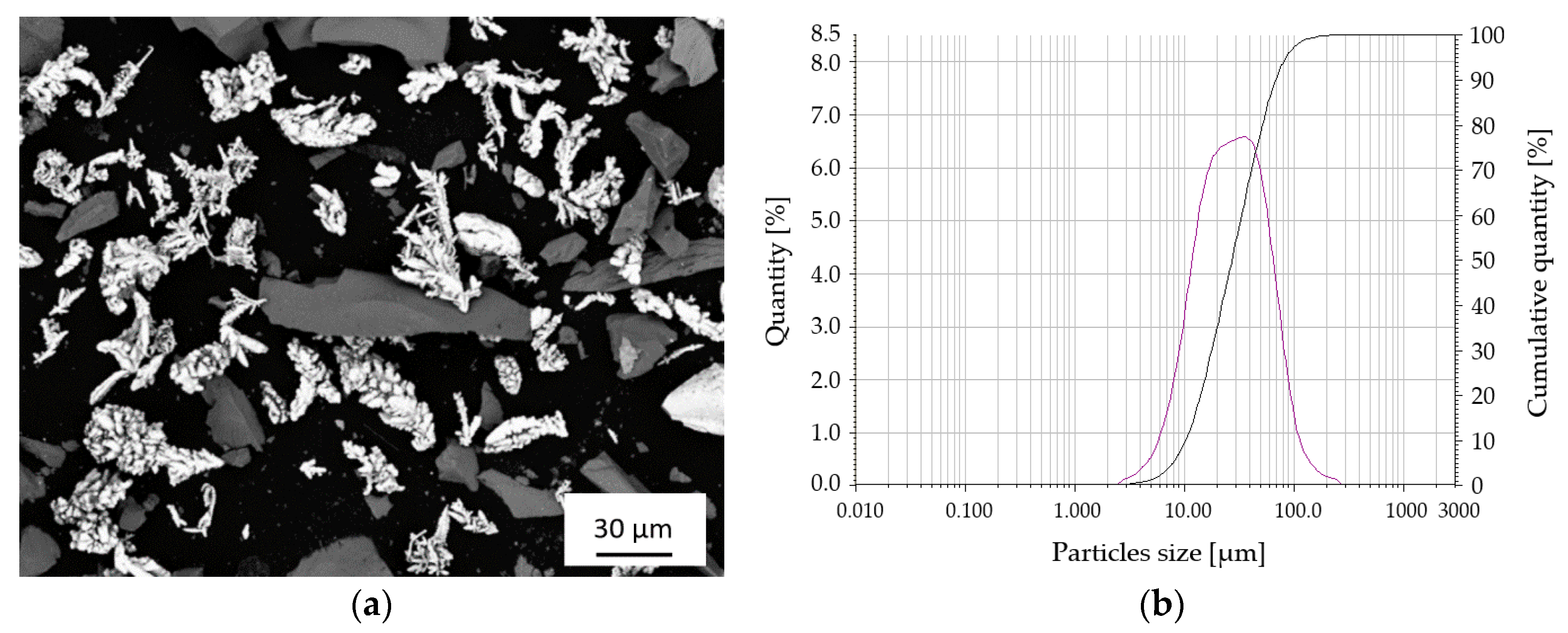
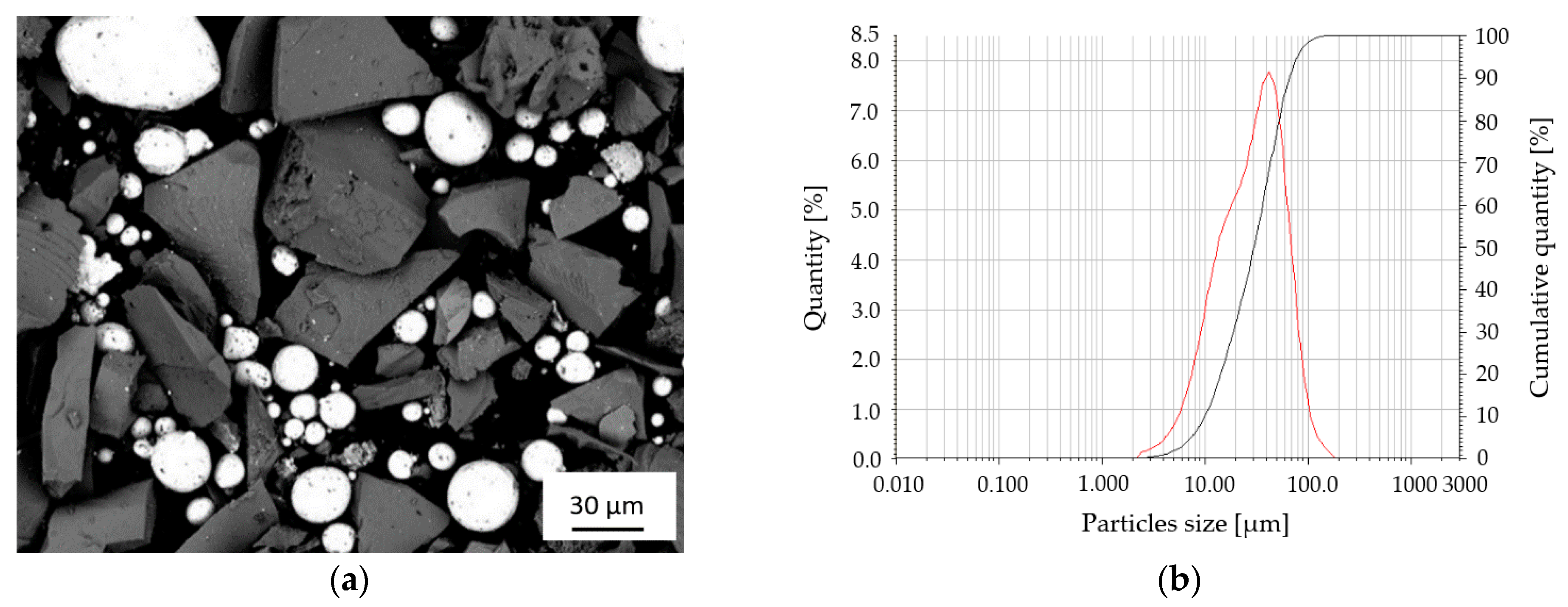
SiC powder, manufactured by crushing with irregular shape and particles size in the range of 15 to 63 µm, was used as ceramic in composite coatings. Metal and ceramic powders were mixed in the weight ratio 1:1. The mixtures are shown in Figure 1a and Figure 2a. Granulometry tester (Analysette 22 MicroTec plus, Fritsch, Markt Einersheim, Kitzingen, Germany) was used to analyze the size of the mixed powders. The results of size distribution are presented in Figure 1b and Figure 2b. Red and violet lines present the number of particles that fall into each of the size ranges, while the black lines express the total number of particles with various sizes, each given as a percentage of the total number in the sample of interest. The powders were sprayed on the S235JR steel substrates of dimensions 15 × 15 × 3 mm3. The substrates were degreased and grit-blasted under a pressure of 0.6 MPa, using alumina powder (mesh 20) to activate the surface, prior to spraying.
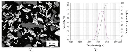
Figure 1.
Scanning electron microscope—SEM (back-scattered electrons—BSE) micrograph of E-Cu/SiC powder (a mixture of dendritic Cu powder and SiC powder) (a) and size analysis of the mixed powders (b).
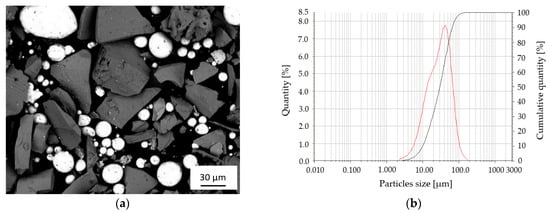
Figure 2.
Scanning electron microscope—SEM (back-scattered electrons—BSE) micrograph of O-Cu/SiC powder (a mixture of spherical Cu powder and SiC powder) (a) and size analysis of the mixed powders (b).
2.2. Spraying Process Parameters
The coatings were deposited using a low-pressure cold spraying unit, Dymet 413 (Obninsk Centre for powder Spraying, Obninsk, Russia), equipped with 3.3 kW internal gas heater in a spraying gun. A standard de Laval nozzle with a tubular shape and an outlet diameter of 5 mm was used. Powder was fed radially, at the beginning of the divergent part of the nozzle. Air was used as a working gas. The spraying gun was attached to a manipulator holder (BZT Maschinenbau GmbH, Leopoldshöhe, Germany). The spray parameters are collected in Table 1. Coating surface topography, thickness, and density strongly depended on the powder material morphology and oxidation level, feeding rate, gas preheating temperature, and pressure [38]. Therefore, to ensure a better comparison of the coatings, both powder mixtures were sprayed with the same parameters. The highest possible gas temperature and pressure for low-pressure cold-sprayed unit were applied to minimize the porosity of the coatings.

Table 1.
Low pressure cold-spraying process parameters.
The design of composite field emitters is shown in Figure 3. The powders were deposited on the substrate surfaces (see Figure 4)—(i) flat and (ii) wavy. A flat coating trajectory consisted of straight longitudinal moves of the spraying gun with a small distance between the beads equal to 2 mm, which resulted in a flat coating surface. In the case of wavy coating trajectory, the spraying gun each stopped 3 mm and moved aside 2 mm to form repeated and multiplied peaks on the surface, while the distance between the next beads was established to be 6 mm. Trajectories of the spray gun for both surfaces are presented in Figure 5. These two extremely different spraying paths were applied to compare the influence of coating surface topography on field emission properties. Both types of coatings were sprayed as a single layer in one manipulator program cycle. SiC powder was additionally sprayed on the surface of some coatings to increase the number of electron emitters. Samples with an extra SiC layer were noted as Cu/SiC + SiC. Table 2 shows all tested coatings.

Figure 3.
Sketch of composite cold-sprayed coating working as a cathode.
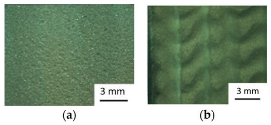
Figure 4.
Morphologies of the deposited coating surfaces—flat (a) and wavy (b).
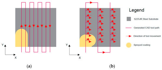
Figure 5.
Planar trajectories of the spraying gun movements used for the deposition of flat (a) and wavy (b) coating.

Table 2.
Collected samples with designation.
2.3. Coatings Characterization
The cross-sections and the surfaces of the coated samples as well as the powder morphology were analyzed using scanning electron microscope—SEM (Tescan VEGA 3 SBH, Brno, Czech Republic), equipped with secondary electrons (SE) and back-scattered electrons (BSE) detectors, as well as the energy-dispersive X-ray spectroscopy (EDX) system enabling elemental analysis. The sizes of particles were analyzed using particle size analyzer Mastersizer 3000 (Malvern Panalytical Ltd., Malvern, UK).
The topography of the as-sprayed samples was characterized using a surface profilometer (Form Talysurf 120 L). The quantity of SiC particles on the surface cross-section of deposited coatings was found by semi-quantitative graphical analysis, using the ImageJ software. Three images with magnification of 1000 were used to estimate the mean value of the SiC phase.
2.4. Field Electron Emission Tests
The externally applied electric field E used in the tests of emission was defined as:
where U [V] and d [μm] are the voltage between cathode and anode and inter-electrode distance, respectively. It should be noted that Equation (1) was only valid when the electric field was applied between two plane-parallel flat surfaces. In real conditions, some irregularities occur on the surface of electrodes causing a local increase of electric field. Those irregularities of the electrode surface become emission points. Local electric field El in the emission point is strictly connected with the macroscopic electric field E by the following equation:
where β is the coefficient of electric field amplification [1/1]. Therefore, the emitter’s surface can be purposefully modified to produce emission points and increase amplification of the electric field.
E = U/d [V/μm]
El = β·E [V/μm]
The emission current I [µA] describing the Fowler-Nordheim (FN) relationship is defined as [43]:
in which α [cm2] and ϕ [eV] are the emitting surface area and work function, respectively.
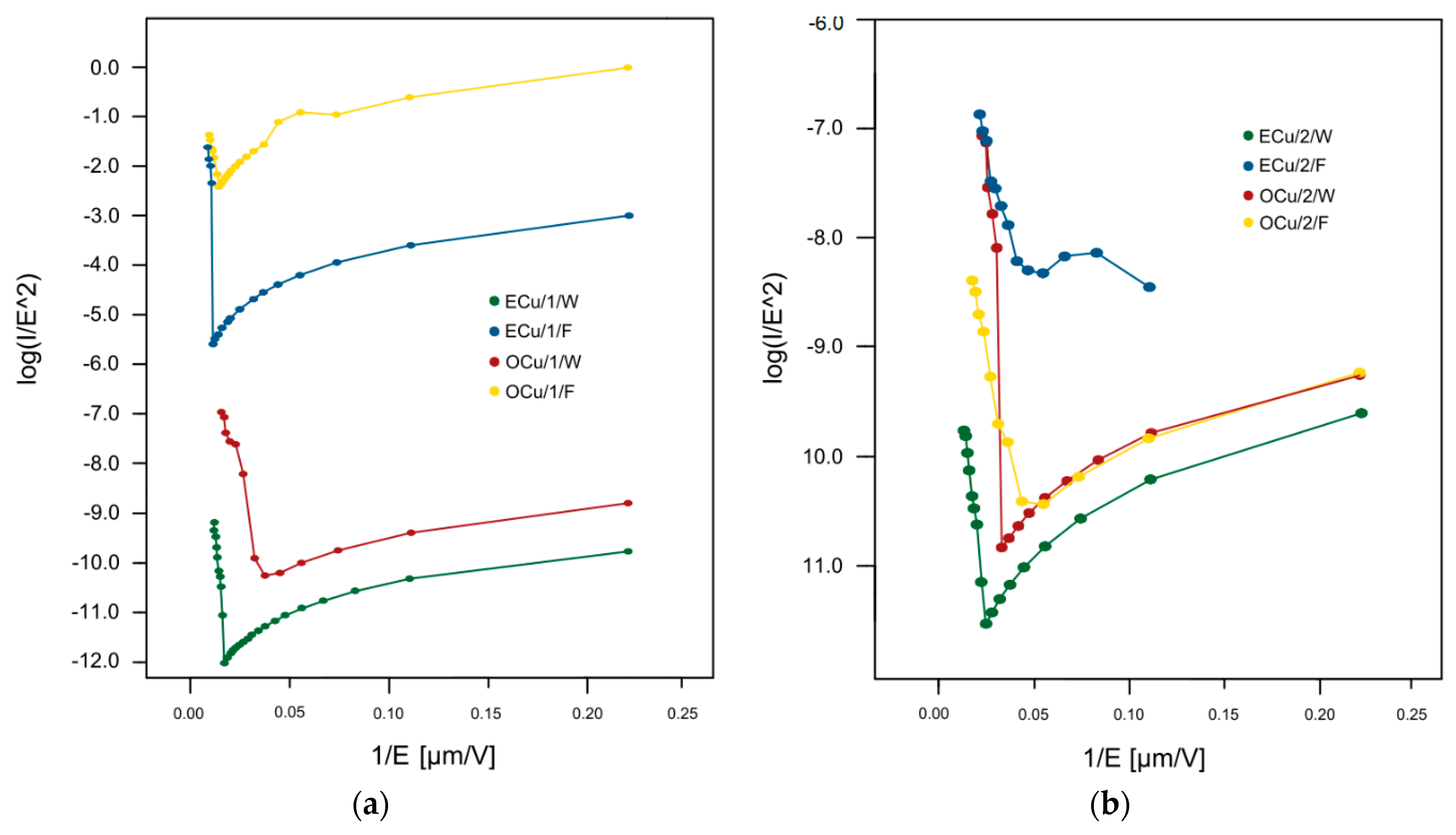
For an easier evaluation of field electron emission properties, e.g., the threshold electric field Eth [V/µm] and the coefficient of β, Equation (3) can be transformed into log(1/E2) as a function of (1/E) and known as the F-N plot [43]:
The relationship is a straight line in the Fowler–Nordheim graphs. The slope of the line depends on the coefficient β, while its y-intercept is determined by the surface area of emission α. Finally, the threshold electric field Eth, which describes the conditions to start electron emission could be estimated.
The tests of field emission were carried out at room temperature in a vacuum chamber, under pressure of 3 . The system included a high-voltage source generating up to 2.5 kV. The current was measured with a Pracitronic MV 40 DC-Milli-Pico-Meter (Präcitronic, Dresden, Germany), while the voltage was measured with an APPA 305 True RMS Multimeter (Appa, New Taipei, Taiwan). The system was protected against electronic noise by a Faraday cage. A hemispherical stainless steel anode of diameter 5 mm was attached in the distance of 25 μm, above the coated samples working as cathode.
3. Results
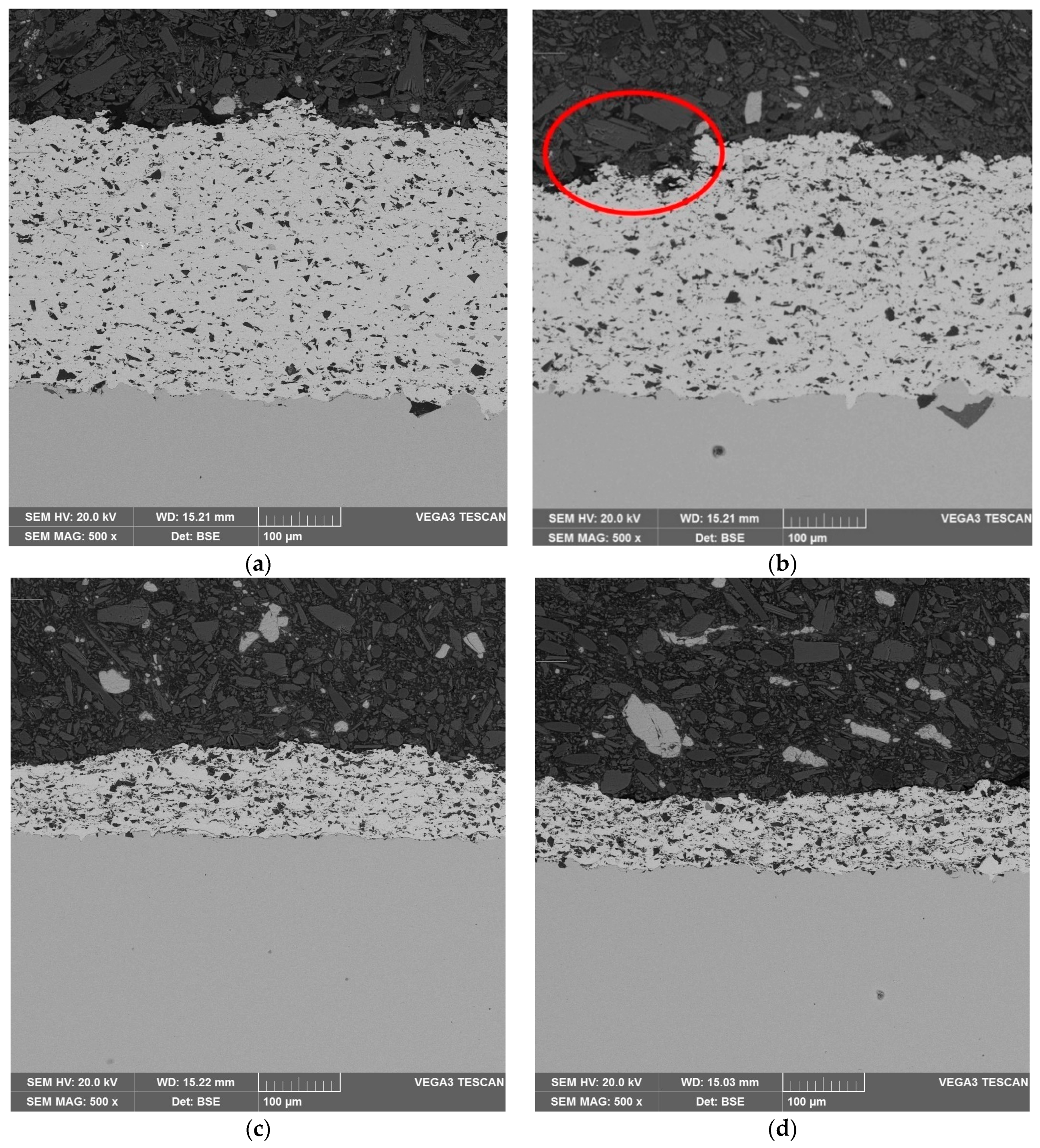
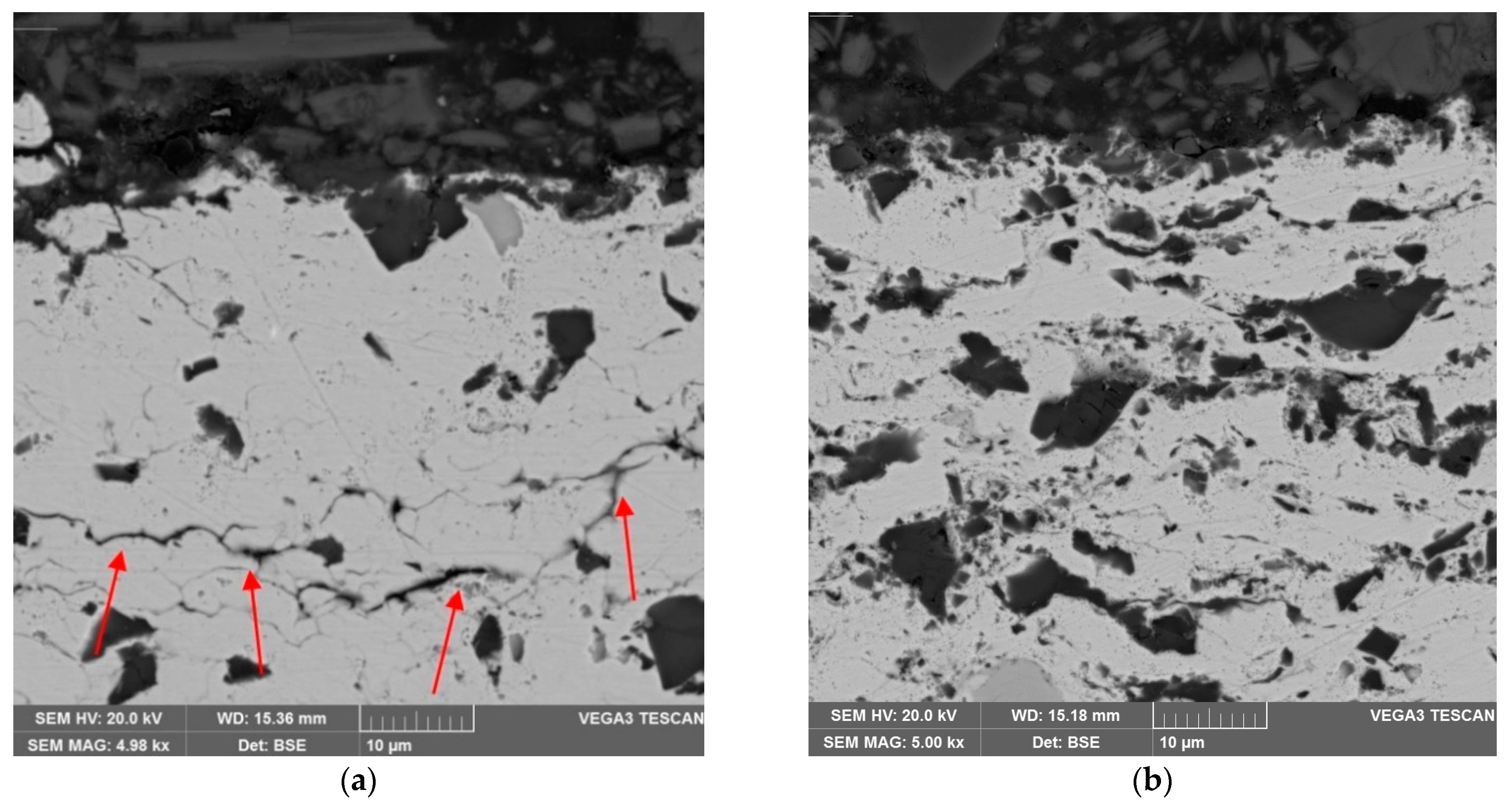
The microstructure of deposited coatings is characterized by high density (Figure 6). Total thickness of the coatings was in the range of 300–450 µm and 80–120 µm for flat or 1200–1800 µm and 300–600 µm for wavy ECu and SCu samples, respectively. Flat and wavy coatings deposited with the use of the same powder mixture showed a similar microstructure. Spraying the layer of pure SiC powder negligibly influenced the thickness of the coatings. Nevertheless, in the case of the ECu/2/F and ECu/2/W samples, pieces of metallic matrix were locally tore off by the incoming ceramic particles, due to an eroding effect (Figure 6b). Moreover, the top part of the coating showed local damage in the form of micro-porosity arising from SiC bombardment (Figure 7a). However, SiC particles cause no defects or material loss in the OCu coatings (Figure 7b). The spherical Cu powder formed more compacted coatings and showed a higher SiC particles content of 24.1% compared to 11.6% in the ECu coatings.

Figure 6.
SEM (BSE) images of ECu (a,b) and SCu (c,d) coatings cross-section without (a,c) or with (b,d) additional SiC layer. Red circle mark the torn off piece of coating.

Figure 7.
SEM (BSE) micrographs of the top part of the ECu/2/F (a) and OCu/2/F (b) coatings. Red arrows mark the damaged region by spraying an additional layer of SiC.
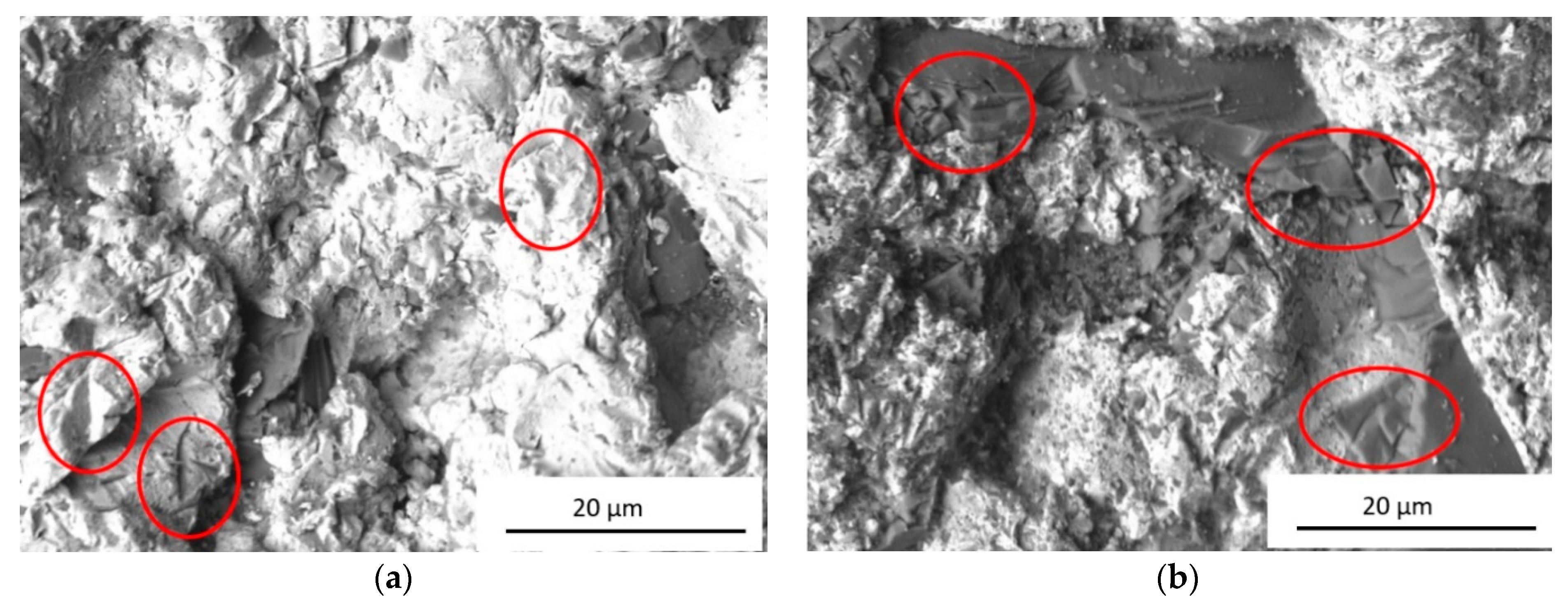
The surface of the as-sprayed coatings is continuous and regular (see Figure 8). The presence of SiC particles is visible in all coating surfaces. Figure 4 shows the topography of surface (flat or wavy) influenced coatings morphology in macroscale. The coatings deposited using powder mixture had a surface with well visible initial particles of copper and silicon carbide (see Figure 9a). A part of ceramic particles should rebound, leaving traces in the metal matrix. The additional spraying of SiC powder did not influence the coatings’ thickness. In fact, the ceramic powder impacted previously deposited coating and were interlocked in the copper matrix. The additional SiC powder resulted in a significant increase of ceramic particles amount on the coatings surface from about 30–38% up to 49–58% for the single-layered and double-layered coatings, respectively (see Table 2). The ceramic particles were crushed at impact leaving a lot of small particles on the coatings’ surface (as shown in Figure 8b), such that the hard particles surely densified the soft copper matrix. The SiC particles increased the as-sprayed coating surface roughness (see Table 2) and these particles had much sharper edges compared to the copper particles. It should be stressed upon that the electric field depended on the emitter apex radius, r, as β ~ 1/r. Consequently, the SiC particles emitted more electrons than copper particles.
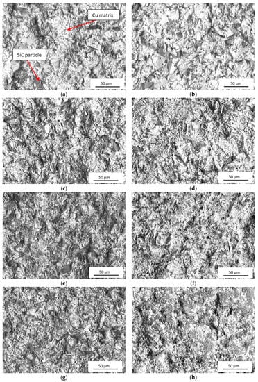
Figure 8.
SEM micrographs (SE) of flat coatings surface—ECu/1/F (a), OCu/1/F (c), ECu/2/F (e), and O-Cu/2/F (g); and wavy coatings surface—ECu/1/W (b), OCu/1/W (d), ECu/2/W (f), and OCu/2/W (h).

Figure 9.
SEM micrograph of flat coatings surface, ECu/1/F (a) and ECu/2/F (b). Red circles mark indents in figure (a) and crushed SiC particles in figure (b).
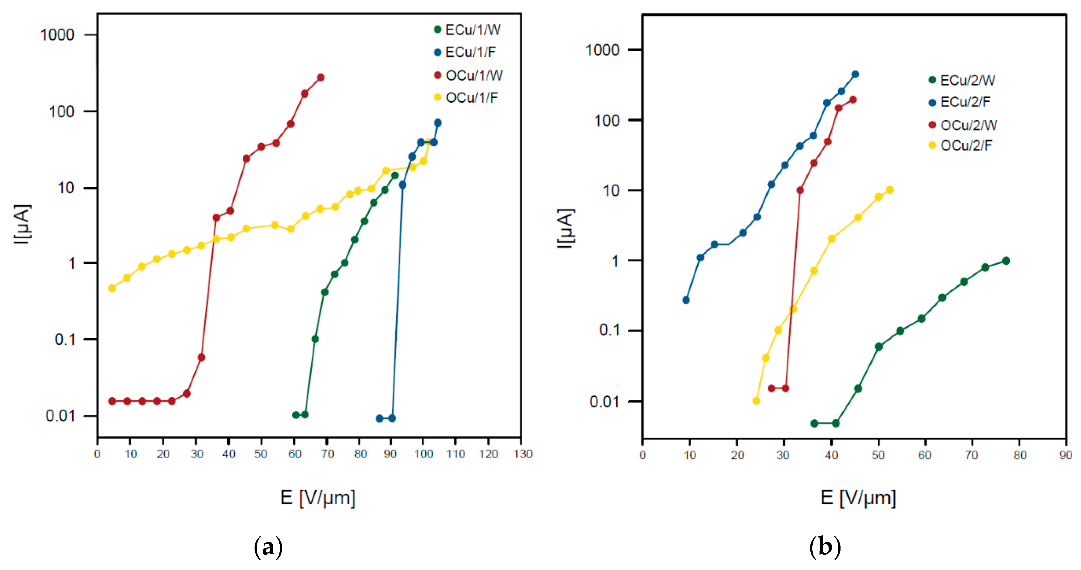
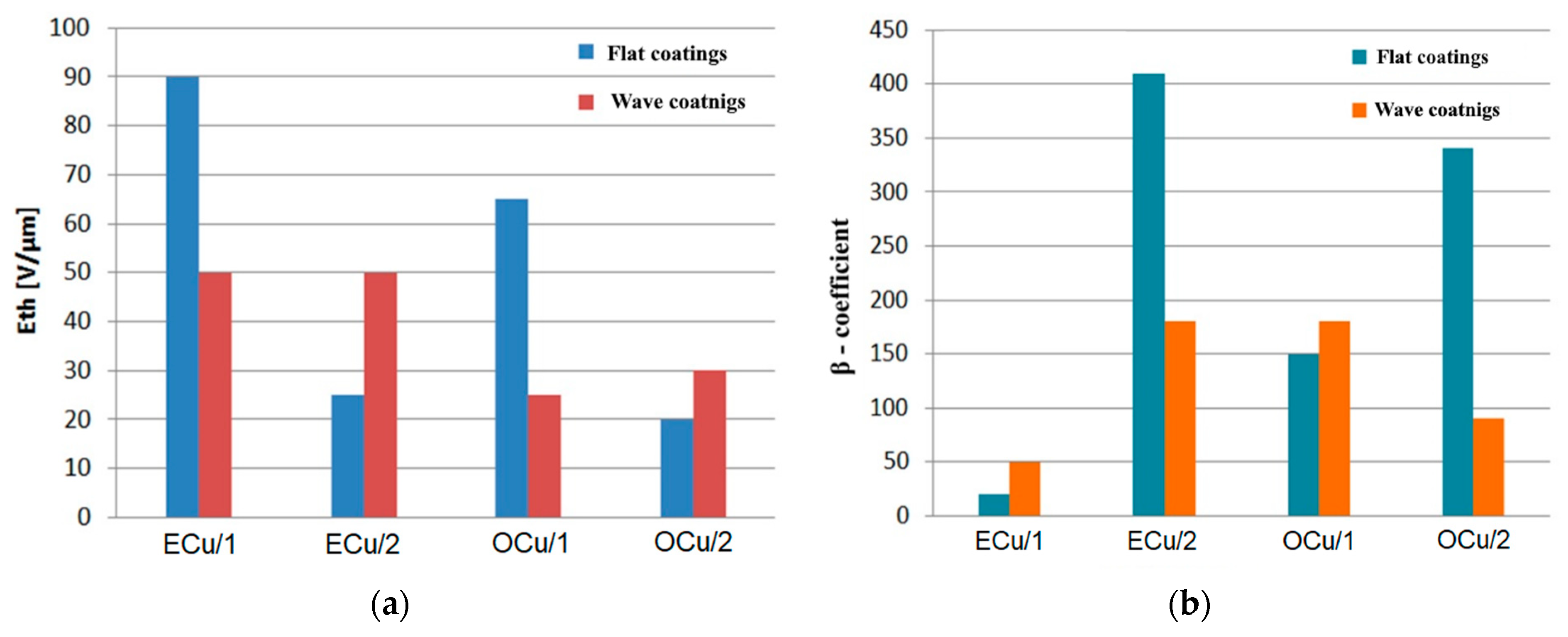
The emission current of the samples in function of voltage, between the anode and the cathode, is proposed by Equation (1) and Fowler–Nordheim graphs described by Equation (2) are shown in Figure 10 and Figure 11, respectively. These figures enabled determining—(i) the coefficient of the electric field amplification, β; (ii) threshold electric field Eth; and (iii) emitting surface, α. Table 3 shows the emitting surface α, while Figure 12 presents the coefficient of electric field amplification and threshold electric field of all tested samples. These parameters enabled describing emission from tested samples, gradually from very weak to very good emission (see Table 3). The best emitters were the samples ECu/2/F and OCu/2/F and the worst ones were samples ECu/1/F and ECu/1/W.
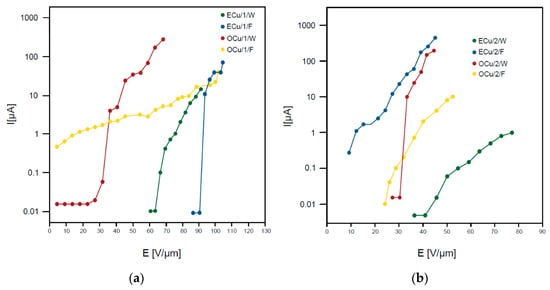
Figure 10.
Emission current vs. voltage between anode and cathode for the single-layered (a) and double-layered (b) samples.
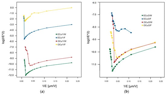
Figure 11.
Fowler-Nordheim graph of the single-layered (a) and double-layered (b) samples.

Table 3.
Composite coatings characterization.
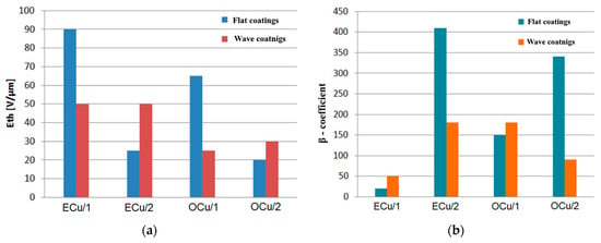
Figure 12.
The threshold electric field, Eth (a) and coefficient of electric field amplification, β (b) of tested samples.
4. Discussion
Cold spray was successfully applied to a deposition of Cu-SiC composite coatings, with a high amount of ceramic particles on the surface. However, despite the same amount of powder feeding rate, coatings showed different thickness. It resulted from a difference in powder morphology and probably oxidation level [44]. Dendritic powder had more developed morphology (see Figure 2), as compared to compacted spherical particles (see Figure 3) and thus was more willing to deform plastically and embed [44]. Nevertheless, spraying an additional layer of SiC resulted in tearing off of metallic particles (Figure 6b and Figure 7a). This effect was not noticed in the OCu coatings characterized by a higher amount of SiC particles in the microstructure. Presence of ceramic strengthens the structure of composite material by increasing the hardness, wear, and erosion resistance [45].
The quality of the tested samples can be divided—in view of electron emission measurement—into two basic groups: (i) good and very good emitters with β coefficient higher than 160; and (ii) weak and very weak emitters with β coefficient lower than 160 (see Table 3). Two outstanding samples, namely ECu/2/F and OCu/2/F belong to the first group (see Figure 8). The coefficients of electric field amplification obtained for these coatings were equal to β = 410 and 340, respectively. These results were comparable to those reported for the best electron emitters, namely, carbon nanotubes, reportedly having a mean value of β ~ 500 [46,47]. On the other hand, the threshold electric fields of the carbon nanotube emitters were in the range of Eth = 5–16 V/μm [8,48,49]. The tested coating samples OCu/2/F had a slightly greater value of this parameter of Eth = 20 V/μm. The samples being weak emitters were e.g., ECu/1/F, ECu/1/W, OCu/1/F, and OCu/2/W. The emission was difficult to initiate and had a high instability, due to insufficient amount of protruding SiC particles and small roughness. The emission was difficult to initiate and had high instability. It should be stressed upon that the materials, such as perovskite as SrTiO3 or ZnIn2S4, could provide a much lower critical field of less than Eth < 9 V/µm or even less than Eth < 1 V/µm, respectively. Some authors, e.g., Roy et al. [27] who tested diamond-like carbon films, found that the emission parameters strongly depended on the deposition conditions and on the microstructure of the films. The authors showed that the critical field of the films varied between Eth = 2 and 28 V/µm and the field amplification coefficient was in the range of β = 4 and 700.
An important factor influencing electron emission was the emitting surface area. The greater emitting surface enabled a reduction of emission current density. The samples assessed as very good emitters, e.g., ECu/2/F and OCu/2/F, had a rather small emitting surface area equal to α = 6.31 × 10⁻¹⁵ and 3.09 × 10⁻¹⁶ cm2, respectively. On the other hand, the coatings with rather weak emission, e.g., ECu/1/F and OCu/1/W (i.e., single-layered coatings), showed a higher value of emitting surface area (see Table 2). The SEM micrographs analysis of the sample surface enabled us to see the difference of morphology between the two groups of emitters (see Figure 8). It was seen that double-layered coatings showed dense packing of small ceramic particles, while in single-layered coatings, the SiC particles were hardly visible. The explanation of this observation could be such that the surfaces with densely packed emitters were characterized by a lower penetration of the electric field, which potentially reduced the coefficient of electric field amplification [50]. This effect is known as the electric field shielding. On the other hand, the sharp edges of the SiC particles in the deposited coatings enabled obtaining high values of β coefficient. Moreover, the field emission occurred from the highest points above the emitter’s surface. Therefore, densely packed sources of electron emission not only cause a decrease of current density, but simultaneously increase the emitter’s life-time. Nevertheless, the OCu/2/W sample showed an excessive decrease of the β coefficient value due to the densification of extremely small SiC particles (see Figure 8h). Protruding and sharply finished particles are desired to improve emission properties. It is stated that presence of waviness disabled deposition of SiC particles with size higher than 10 µm, limiting the number of highest points above the coating surface. Further research is needed to determine optimal size of SiC particles in cold-sprayed coatings dedicated for field electron emitters.
5. Conclusions
The paper presents the technology of Cu-SiC composite coatings deposited onto S235JR steel through low-pressure cold spraying. Two morphologies of copper powders, i.e., dendritic and spherical, were used. These powders were mixed with crushed SiC ceramic powder. The powders were sprayed to form regular and continuous coatings. Some of the as-sprayed coatings were covered with additional SiC layer. These coatings showed that many SiC particles were implanted on the surface. Two types of coating shapes were designed—(i) flat and (ii) wavy. SEM analysis of coating surfaces confirmed the implantation of SiC particles in coatings with additional SiC layer. All examined emitters showed a relatively stable emission. The field emission characteristics were influenced by the quantity and shape of SiC particles. The tested samples could be divided into two basic groups—(i) good and very good emitters, and (ii) weak or very weak emitters. The first group included two outstanding samples of E-Cu/SiC + SiC and O-Cu/SiC + SiC, which had flat coatings with a threshold field Eth of 20 V/µm and 24 V/µm and β coefficient of 340 and 410, respectively.
Author Contributions
Conceptualization, M.W. and Z.Z.; methodology M.W. and Z.Z.; software, M.W.; validation, M.W. and Z.Z.; formal analysis, M.W. and W.Ł.; investigation, M.W. and Z.Z.; resources, M.W. and Z.Z.; data curation, M.W. and W.Ł.; writing—original draft preparation, M.W. and W.Ł.; writing—review and editing, M.W. and W.Ł.; visualization, M.W.; supervision, M.W. and Z.Z.; project administration, M.W.; funding acquisition, M.W. All authors have read and agreed to the published version of the manuscript.
Funding
This research was funded by Polish National Science Centre, grant number 2016/23/D/ST8/00675 (Project title: The mechanism of joining submicron ceramic particles in cold spraying process).
Institutional Review Board Statement
Not applicable.
Informed Consent Statement
Not applicable.
Data Availability Statement
The data presented in this study are available.
Acknowledgments
The authors thank to Lech Pawłowski for help in redaction and for many useful discussions.
Conflicts of Interest
The authors declare no conflict of interest.
References
- Anguero, V.M.; Adamo, R.C. Space Applications of Spindt Cathode Field Emission Arrays. In Proceedings of the 6th Space-Craft Charging Conference, Hanscom AFB, MA, USA, 2–6 November 1998; pp. 347–352. [Google Scholar]
- Matéo-Vélez, J.-C.H.; Belhaj, M.; Roussel, J.-F.; Rodgers, D.; Cipriani, F. Design and Numerical Assessment of a Passive Electron Emitter for Spacecraft Charging Alleviation. IEEE Trans. Plasma Sci. 2015, 43, 2839–2848. [Google Scholar] [CrossRef]
- Fléron, R.A.W.; Blanke, M. Electron Emitter for Small-Size Electrodynamic Space-Tether Using Mems Technology. In Proceedings of the ESA Symposium on Small Spacecraft Systems, La Rochelle, France, 20–24 September 2004; European Space Agency: Noordwijk, The Netherlands, 2004; pp. 227–232. [Google Scholar]
- Czarczynski, W.; Znamirowski, Z. Field electron emission experiments with plasma sprayed layers. Surf. Coat. Technol. 2008, 202, 4422–4427. [Google Scholar] [CrossRef]
- Spindt, C.A. A Thin-Film Field-Emission Cathode. J. Appl. Phys. 1968, 39, 3504–3505. [Google Scholar] [CrossRef]
- Luo, J.; Liu, L.; Sun, F.; Tang, X.; Zheng, R.-T.; Wu, X.-L.; Cheng, G.-A. Effect of purification methods on the cross-sectional field emission properties of carbon nanotube and graphene composite films. Diam. Relat. Mater. 2020, 106, 107848. [Google Scholar] [CrossRef]
- Shiroishi, T.; Hosono, A.; Sono, A.; Nishimura, K.; Suzuki, Y.; Nakata, S.; Okuda, S. Improvement of emission characteristics uniformity of carbon nanotube field emission display by surface treatment. J. Vac. Sci. Technol. B Microelectron. Nanometer Struct. 2006, 24, 979. [Google Scholar] [CrossRef]
- Kimura, C.; Yamamuro, Y.; Aoki, H.; Sugino, T. Improved field emission characteristics of carbon nanofiber treated with nitrogen plasma. Diam. Relat. Mater. 2007, 16, 1383–1387. [Google Scholar] [CrossRef]
- Forbes, R.G. Low-macroscopic-field electron emission from carbon films and other electrically nanostructured heterogeneous materials: Hypotheses about emission mechanism. Solid-State Electron. 2001, 45, 779–808. [Google Scholar] [CrossRef]
- Sunab, L.; Chenb, E.; Guob, T. Field emission enhancement of composite structure of ZnO quantum dots and CuO nanowires by Al2O3 transition layer optimization. Ceram. Int. 2020, 46, 15565–15571. [Google Scholar] [CrossRef]
- Wu, X.; Wang, Y.; Yang, P. The field emission properties from the pristine/B-doped graphene–C 70 composite. Phys. Lett. A 2017, 381, 2004–2009. [Google Scholar] [CrossRef]
- Wu, Y.; Li, J.; Ye, J.; Song, Y.; Chen, X.; Huang, S.; Sun, Z.; Ou-Yang, W. Outstanding field emission properties of titanium dioxide /carbon nanotube composite cathodes on 3D nickel foam. J. Alloys Compd. 2017, 726, 675–679. [Google Scholar] [CrossRef]
- Litovchenko, V.; Evtukh, A.; Kryuchenko, Y.; Goncharuk, N.; Yilmazoglu, O.; Mutamba, K.; Hartnagel, H.; Pavlidis, D. Quantum-size resonance tunneling in the field emission phenomenon. J. Appl. Phys. 2004, 96, 867–877. [Google Scholar] [CrossRef]
- Wang, H.; Jiang, W.; Kang, L.; Li, Z. Photoluminescence and electron field-emission properties of SiC-SiO2 core-shell fibers and 3C–SiC nanowires on silicon nanoporous pillar array. J. Alloys Compd. 2013, 553, 125–128. [Google Scholar] [CrossRef]
- Matallana, A.; Ibarra, E.; López, I.; Andreu, J.; Garate, J.; Jordà, X.; Rebollo, J. Power module electronics in HEV/EV applications: New trends in wide-bandgap semiconductor technologies and design aspects. Renew. Sustain. Energy Rev. 2019, 113. [Google Scholar] [CrossRef]
- Lelis, A.J.; Green, R.; Habersat, D.B.; El, M. Basic Mechanisms of Threshold-Voltage Instability and Implications for Reliability Testing of SiC MOSFETs. IEEE Trans. Electron Devices 2015, 62, 316–323. [Google Scholar] [CrossRef]
- Masri, P. Silicon carbide and silicon carbide-based structures. Surf. Sci. Rep. 2002, 48, 1–51. [Google Scholar] [CrossRef]
- Buttay, C.; Planson, D.; Allard, B.; Bergogne, D.; Bevilacqua, P.; Joubert, C.; Lazar, M.; Martin, C.; Morel, H.; Tournier, D.; et al. State of the art of high temperature power electronics. Mater. Sci. Eng. B 2011, 176, 283–288. [Google Scholar] [CrossRef]
- Ying, P.-Z.; Chen, S.; Ren, X.-L.; Chen, Q. Investigation of temperature on the field electron emission from flexible N-doped SiC nanoneedles. Superlattices Microstruct. 2015, 86, 250–255. [Google Scholar] [CrossRef]
- Deng, J.-H.; Sun, P.-C.; Cheng, G.-A.; Zheng, R. Improved field electron emission from SiC assisted carbon nanorod/nanotube heterostructured arrays by using energetic Si ion irradiation. Surf. Coat. Technol. 2013, 228, S323–S327. [Google Scholar] [CrossRef]
- Winnicki, M.; Malachowska, A.; Baszczuk, A.; Rutkowska-Gorczyca, M.; Kukla, D.; Lachowicz, M.; Ambroziak, A. Corrosion protection and electrical conductivity of copper coatings deposited by low-pressure cold spraying. Surf. Coat. Technol. 2017, 318, 90–98. [Google Scholar] [CrossRef]
- Kumar, S.D.; Ravichandran, M.; Sakthivelu, S.; Meignanamoorthy, M.; Chanakyan, C.; Alagarsamy, S. Mechanical properties of magnesium-silicon carbide composite fabricated through powder metallurgy route. Mater. Today Proc. 2020, 27, 1137–1141. [Google Scholar] [CrossRef]
- Kee, S.-H.; Kim, W.-J.; Jung, J.-P. Copper-silicon carbide composite plating for inhibiting the extrusion of through silicon via (TSV). Microelectron. Eng. 2019, 214, 5–14. [Google Scholar] [CrossRef]
- Chmielewski, M.; Nosewicz, S.; Wyszkowska, E.; Kurpaska, Ł.; Strojny-Nędza, A.; Piątkowska, A.; Bazarnik, P.; Pietrzak, K. Analysis of the micromechanical properties of copper-silicon carbide composites using nanoindentation measurements. Ceram. Int. 2019, 45, 9164–9173. [Google Scholar] [CrossRef]
- Kaur, G.; Kumar, R.; Lahiri, I. Field electron emission from protruded GO and rGO sheets on CuO and Cu nanorods. Phys. E Low-Dimens. Syst. Nanostruct. 2019, 112, 10–18. [Google Scholar] [CrossRef]
- Tzeng, Y.; Liu, C.; Hirata, A. Effects of oxygen and hydrogen on electron field emission from microwave plasma chemically vapor deposited microcrystalline diamond, nanocrystalline diamond, and glassy carbon coatings. Diam. Relat. Mater. 2003, 12, 456–463. [Google Scholar] [CrossRef]
- Roy, R.; Gupta, S.; Deb, B.; Pal, A. Electron field emission properties of electro-deposited diamond-like carbon coatings. Vacuum 2003, 70, 543–549. [Google Scholar] [CrossRef]
- Zhai, C.; Yun, J.; Zhao, L.; Zhang, Z.; Wang, X.-W.; Chen, Y. Effect of annealing on field emission properties of nanodiamond coating. Phys. B Condens. Matter 2011, 406, 1124–1128. [Google Scholar] [CrossRef]
- Waldmann, O.; Persaud, A.; Kapadia, R.; Takei, K.; Allen, F.I.; Javey, A.; Schenkel, T. Effects of palladium coating on field-emission properties of carbon nanofibers in a hydrogen plasma. Thin Solid Films 2013, 534, 488–491. [Google Scholar] [CrossRef]
- Jiang, R.; Zeng, B.; Liu, J.; Chai, X.; Chen, T.; Wu, Z.; Zhang, X.; Yang, K. Enhanced field electron emission of single-walled carbon nanotubes prepared by imprinting technique. J. Alloys Compd. 2020, 816, 152669. [Google Scholar] [CrossRef]
- Bankar, P.K.; Kolhe, P.S.; Mutadak, P.R.; Kawadeb, A.; Sonawane, K.M.; More, M.A. Evaluation of field electron emission properties of ZnIn2S4 nanopetals grown on conducting carbon substrate. Phys. E Low-Dimens. Syst. Nanostruct. 2021, 125, 114363. [Google Scholar] [CrossRef]
- Yang, Y.; Wang, L.-J.; Wang, X.-P.; Chen, J.-X.; Yang, X.-W.; Li, M.-H.; Deng, M.-J. Perovskite-type SrTiO3 thin film preparation and field emission properties. Vacuum 2020, 178, 109466. [Google Scholar] [CrossRef]
- Li, J.; Luo, Z. Fabrication and performances of preceramic polymer-based high-temperature High emissivity coating. J. Eur. Ceram. Soc. 2020, 40, 5217–5225. [Google Scholar] [CrossRef]
- Wang, X.-P.; Li, M.-H.; Guo, M.-M.; Wang, L.-J.; Yang, X.-W.; Yang, Y.; Deng, G.-R.M.-J.; Yang, G.-R.; Qian, Y.-T. Effect of metal coating material on field emission of vertically grown layered MoS2 nanosheets. Vacuum 2020, 177, 109386. [Google Scholar] [CrossRef]
- Znamirowski, Z.; Pawłowski, L.; Cichy, T.; Czarczynski, W. Low macroscopic field electron emission from surface of plasma sprayed and laser engraved TiO2, Al2O3+13TiO2 and Al2O3+40TiO2 coatings. Surf. Coat. Technol. 2004, 187, 37–46. [Google Scholar] [CrossRef]
- Tomaszek, R.; Znamirowski, Z.; Pawlowski, L.; Zdanowski, J. Effect of Conditioning on Field Electron Emission of Sus-pension Plasma Sprayed TiO2 Coatings. Vacuum 2007, 81, 1278–1282. [Google Scholar] [CrossRef]
- Znamirowski, Z.; Ladaczek, M. Lighting segment with field electron titania cathode made using suspension plasma spraying. Surf. Coat. Technol. 2008, 202, 4449–4452. [Google Scholar] [CrossRef]
- Champagne, V.K. The Cold Spray Materials Deposition Process, 1st ed.; Woodhead Publishing Ltd.: Cambridge, UK, 2007. [Google Scholar]
- Assadi, H.; Schmidt, T.; Richter, H.; Kliemann, J.-O.; Binder, K.; Gärtner, F.; Klassen, T.; Kreye, H. On Parameter Selection in Cold Spraying. J. Therm. Spray Technol. 2011, 20, 1161–1176. [Google Scholar] [CrossRef]
- Li, C.-J.; Wang, H.-T.; Zhang, Q.; Yang, G.-J.; Li, W.-Y.; Liao, H.L. Influence of Spray Materials and Their Surface Oxidation on the Critical Velocity in Cold Spraying. J. Therm. Spray Technol. 2009, 19, 95–101. [Google Scholar] [CrossRef]
- Wang, Y.; Normand, B.; Mary, N.; Yu, M.; Liao, H. Microstructure and corrosion behavior of cold sprayed SiCp/Al 5056 composite coatings. Surf. Coat. Technol. 2014, 251, 264–275. [Google Scholar] [CrossRef]
- Arrabal, R.; Pardo, A.; Merino, M.C.; Mohedano, M.; Casajús, P.; Merino, S. Al/SiC thermal spray coatings for corrosion protection of Mg-Al alloys in humid and saline environments. Surf. Coat. Technol. 2010, 204, 2767–2774. [Google Scholar] [CrossRef]
- Altman, I.S.; Pikhitsa, P.V.; Choi, M. Electron field emission from nanocarbons: A two-process model. Appl. Phys. Lett. 2004, 84, 1126–1128. [Google Scholar] [CrossRef]
- Schmidt, T.; Gärtner, F.; Assadi, H.; Kreye, H. Development of a generalized parameter window for cold spray deposition. Acta Mater. 2006, 54, 729–742. [Google Scholar] [CrossRef]
- Szala, M.; Łatka, L.; Walczak, M.; Winnicki, M. Comparative study on the cavitation erosion and sliding wear of cold-sprayed Al/Al2O3 and Cu/Al2O3 coatings, and stainless steel, aluminium alloy, copper and brass. Metals 2020, 10, 856. [Google Scholar] [CrossRef]
- Teo, K.B.K.; Lee, S.-B.; Chhowalla, M.; Semet, V.; Binh, V.T.; Groening, O.; Castignolles, M.; Loiseau, A.; Pirio, G.; Legagneux, P.; et al. Plasma enhanced chemical vapour deposition carbon nanotubes/nanofibres how uniform do they grow? Nanotechnology 2003, 14, 204–211. [Google Scholar] [CrossRef]
- Milne, W.; Teo, K.; Chhowalla, M.; Amaratunga, G.; Pribat, D.; Legagneux, P.; Pirio, G.; Binh, V.T.; Semet, V. Electron emission from arrays of carbon nanotubes/fibres. Curr. Appl. Phys. 2002, 2, 509–513. [Google Scholar] [CrossRef]
- Su, C.-Y.; Juang, Z.-Y.; Chen, Y.; Leou, K.; Tsai, C. The field emission characteristics of carbon nanotubes coated by boron nitride film. Diam. Relat. Mater. 2007, 16, 1393–1397. [Google Scholar] [CrossRef]
- Hong, X.; Zheng, H.; Liang, D. Stable electron field emission from graphene/hexagonal boron nitride hybrid structure. Mater. Lett. 2020, 277, 128356. [Google Scholar] [CrossRef]
- Znamirowski, Z.; Posadowski, W.; Pawłowski, L.; Cattini, A.; Latka, L. Electron emission from the zirconium coated suspension plasma sprayed bioglass. Surf. Coat. Technol. 2015, 268, 63–69. [Google Scholar] [CrossRef]
Publisher’s Note: MDPI stays neutral with regard to jurisdictional claims in published maps and institutional affiliations. |
© 2021 by the authors. Licensee MDPI, Basel, Switzerland. This article is an open access article distributed under the terms and conditions of the Creative Commons Attribution (CC BY) license (http://creativecommons.org/licenses/by/4.0/).

