Article

Research on Material Removal Mechanism of Micro-EDM in Deionized Water

1
Key Laboratory of Laser Green Intelligent Manufacturing Technology, Qingdao University of Technology, Qingdao 266525, China
2
Qingdao Haijian Energy Conservation and Environmental Protection Co., Ltd., Qingdao 266235, China
3
Dong Fang International Container (Qingdao) Co., Ltd., Qingdao 266500, China
*
Author to whom correspondence should be addressed.
Coatings 2021, 11(3), 322; https://doi.org/10.3390/coatings11030322
Submission received: 8 February 2021 / Revised: 8 March 2021 / Accepted: 8 March 2021 / Published: 11 March 2021

Abstract

:
As one of the most promising processing methods, the microelectrical discharge machining (micro-EDM) process is widely used in industrial production; however, the material removal mechanism of micro-EDM in deionized water has not been clarified due to scale effect. In this paper, the influence of discharge parameters on the discharge crater size was studied by means of a single-pulse discharge experiment using a resistor–capacitor circuit (RC circuit). The variation trend of the discharge crater size with open-circuit voltage and capacitance was discussed based on the experimental results. The results show that the diameter and depth of the discharge crater increases with capacitance and open-circuit voltage due to the increasing discharge duration and the energy density of the discharge plasma. The discharge energy increases with the increase of capacitance and open-circuit voltage, which causes more materials to melt and vaporize, leading to the crater volume becoming larger. This study has reference value for the further application of micro-EDM adopting deionized water as a dielectric.

1. Introduction

Due to the advantage of being suitable for machining hard materials and complex shape geometries, the electrical discharge machining (EDM) process is applied to produce injection molds, forging and aircraft parts [1,2], etc. The material removal during the EDM process is based on the electrothermal corrosion between the workpiece and the tool (positive and negative electrodes) immersed in the dielectric, until the predetermined processing requirements for the size, shape, and surface quality of metal parts are met. EDM oil is adopted as dielectric by lots of reports. During the EDM process, the material at the discharge point of metal workpiece and tool melt and vaporize rapidly, and the dielectric between workpiece and tool also evaporates and decomposes rapidly [3]. Due to its especial machining mechanism, electromagnetic radiation and harmful gas emission in the EDM process are more serious than traditional machining methods [4]. The gas emitted is harmful to the human nervous system, cardiovascular system, respiratory system, vision, and skin tissue [5]. The composition of smoke emission during the EDM process is related to the material and viscosity of the tool, workpiece, and insulating dielectric.
An effective method to reduce pollution is adopting deionized water as a dielectric. Baroi et al. [6] studied the machining characteristics of EDM in hydrocarbon oil and deionized water. They indicated that deionized water can reduce toxic emissions effectively compared to hydrocarbon oil. Nguyen et al. [7] indicated that deionized water is a relatively low-cost and eco-friendly dielectric fluid owing to the higher material removal rate and lower tool wear than hydrocarbon oil. Chung et al. [8] found that the surface roughness of micro hole surfaces processed by micro-EDM in deionized water can be reduced to 0.066 µm. Yu and Kunieda [9] indicated that higher machining efficiency can be obtained when adopting deionized water as a dielectric because the water can be decomposed into oxygen during arc discharge, which would accelerate the oxidation of electrode materials. However, the material removal mechanism of micro-EDM is extremely complex, as it is different from conventional EDM due to the very short discharge duration and very small discharge gap. The discharge characteristic and material removal mechanism of micro-EDM in deionized water has still not been clarified [10]. Therefore, it is necessary to further clarify the machining mechanism of micro-EDM in deionized water.
As the machining process of micro-EDM can be divided into single-pulse discharge, it is a simple and effective method for analyzing single-pulse discharge characteristics instead of continuous discharge machining performance [11,12]. The energy efficiency and machinability of micro-EDM can be evaluated by studying the characteristics of a single discharge [13]. In addition, the machining process can be optimized by developing predictive models when collecting the effective number of spark discharges [14]. Therefore, it is very important to clarify the material erosion characteristics of the single-pulse discharge for improving the machining characteristics of micro-EDM. In this paper, an electrothermal model is analyzed, and the experimental study of a single-pulse discharge using resistor–capacitor circuit (RC circuit) is conducted. The variation trend of the discharge crater size with open-circuit voltage and capacitance is discussed in relation to the experimental results.

2. Materials and Methods

2.1. Electrothermal Model

The material is eroded by the instantaneous high pressure and high temperature produced by the discharge plasma channel of micro-EDM [15]. During each effective discharge, the dielectric between the tool and the workpiece electrode is broken down to form a plasma channel. The instantaneous high temperature and high pressure generated by the plasma channel make the electrode material at the discharge point melt and vaporize rapidly. Under the action of thermodynamics, electrodynamics, and hydrodynamics, all the vaporized material and partially melted material are thrown away from the electrode surface, and a part of melted material is solidified again to form the discharge crater with a recast layer after the discharge. This is the recognized material removal process. Actually, there is material removed during each discharge, and the EDM process is composed of numerous continuous single pulse discharges.
The schematic diagram of the thermal conduction of the discharge point in workpiece material is as shown in Figure 1. The transient Fourier heat conduction equation involving a single spark discharge can be expressed as:
1 α T t = 2 T z 2 + 2 T r 2 + 1 r T r
where   t is the discharge duration (s), z is the vertical distance (m), α is the thermal diffusivity (m2/s), r is the radial distance (m), and T represents the temperature distribution, T = f r , z , t .
When assumed that all the melted material at the discharge point during EDM is eroded, the thermal diffusivity can be modified by taking the latent heat of melting into consideration, and the expression is written as:
α = K t ρ C p + L m / T m
where K t is the thermal conductivity of the workpiece (W/(m·K)), C p is the specific heat of the material, L m is the latent heat of melting (kJ/mol), ρ is the density of workpiece, and T m represents the melting point (K).
However, most of the material is removed by vaporization due to the high energy density and ultra-short discharge duration of micro-EDM [16]. Therefore, the latent heat of vaporization has significant influence on the material removal. Equation (2) can be rewritten as:
α = K t ρ C p + L m + L v / ( T v T 0
where T 0 is the ambient temperature ( T 0 = 293 K), T v is the vaporization temperature (K), and L v represents the latent heat of vaporization (kJ/mol).
By means of a Hankel transformation and Laplace transformation, Equation (1) can be solved as [17]:
T r , z , t = 2 Q f α t K t i e r f c z 2 α t i e r f c z 2 + R 2 2 α t e r 2 4 α t
where i e r f c represents the complementary error function, R represents the radius of the discharge plasma (m), and Q f represents the heat flux of the discharge plasma.
The heat flux of discharge plasma   Q f can be represented as:
Q f = μ U I / π R 2
where U represents the discharge voltage (V), μ represents the energy distribution rate, I represents the discharge electric current (A), and R represents the radius of the discharge plasma (m).
Thus, Equation (4) can be rewritten as:
T r , z , t = 2 μ U I α t π R 2 K t i e r f c z 2 α t i e r f c z 2 + R 2 2 α t e r 2 4 α t
From Equation (6), it can be noticed that the temperature gradient is proportional to the discharge voltage and discharge electric current when the thermal characteristics are kept constant. Since the higher temperature gradient causes the material to erode more easily, the material erosion of micro-EDM depends on the discharge voltage and discharge electric current. It was indicated that the material removal rate of micro-EDM increases with the discharge voltage and peak current [18]. When the discharge voltage or discharge electric current becomes higher, the size of the discharge crater becomes larger, and the material removal rate becomes higher.

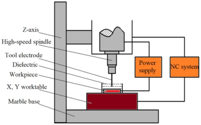
2.2. Experimental Setup

The micro-EDM platform that was adopted to conduct the single-pulse discharge experiments is as shown in Figure 2.
The resolution of the servo feed system was 0.2 mm, which was driven by a precision servo motor (BX4 Cx, FAULHABER Corp., Clearwater, FL, USA) The power supply consists of a direct current (DC) power supply and a resistor–capacitor circuit (RC circuit), which can adjust discharge energy by changing the capacitance and open-circuit voltage. A tungsten rod with diameter of 0.5 mm that was fastened to a rotating spindle was adopted as the tool electrode (the rotation speed was kept as 2000 rpm). Austenitic stainless steel (AISI 304, TISCO, Taiyuan, China) with thickness of 0.3 mm was used as the workpiece. Deionized water was used as a dielectric. The polarity of the tool and workpiece was negative and positive, respectively. The material of the worktable was marble to minimize the effect of parasitic capacitance. The main discharge parameters are listed in Table 1.

2.3. Experimental Procedure

The interelectrode voltage was monitored by an oscilloscope (DSO-X2024A, Agilent, CA, USA). Before the experiment, we allowed the tool to contact the surface of the workpiece, and then we adjusted the gap between the tool and the workpiece electrode to 20 µm. We fed the tool step by step after the intended discharge parameters were set. Once discharge occurred, we returned the tool to original position and prepared for the next discharge. The single factor experimental method was adopted in this study, while the open-circuit voltage and capacitance were selected as variables. The experiments were conducted by changing only one parameter (open-circuit voltage or capacitance) when the other parameters were kept constant. Each discharge was repeated three times, and the average value was taken as result. The surface topography of the discharge crater was observed and measured by an optical microscopy system (MX-6R, EAST IMAGE, Shanghai, China). The picture of the discharge crater is as shown in Figure 3.

3. Results and Discussion

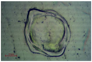
3.1. Influence of Discharge Energy on Discharge Crater Diameter

Figure 4 shows the evolutions of the discharge crater diameter with open-circuit voltage and discharge energy. As shown in Figure 4a, the diameter of the discharge crater increases with the open-circuit voltage, regardless of capacitance. This is because the higher the open-circuit voltage, the larger the gap between tool and workpiece electrodes. The larger discharge gap leads to the larger diameter of the discharge plasma, which causes a larger heat source diameter and discharge crater diameter. In addition, it can be found that the diameter of the discharge crater increases with capacitance when the open-circuit voltage is kept constant. The larger the capacitance, the longer the discharge duration; thus, there is more energy consumed in the production of a discharge crater. As a result, the diameter of the discharge crater is larger when the capacitance is higher.
In the case of the RC circuit, the discharge energy W of each discharge can be estimated by
W = 1 2 C U c 2
where U c represents the open-circuit voltage (V), and C represents the capacitance (nF).
From Equation (7), it can be noted that the discharge energy W increases as the open-circuit voltage and capacitance increased. During spark discharge, there is only a portion of discharge energy that is consumed for material erosion, while the rest is lost owing to ionization, light, radiation and heat conduction [11]. However, even if the energy distribution ratio is constant, the higher the total discharge energy, the more the energy that is transmitted to the electrode for melting and vaporization. Therefore, the higher the open-circuit voltage and capacitance, the larger the discharge energy, and thus there is more material being eroded. As a result, it can be observed from Figure 4b that the discharge crater diameter significantly increases as the discharge energy increased. The minimum diameter of the discharge crater is 0.85 µm when the discharge energy is 4.5 × 10⁻⁵ mJ, while the maximum diameter of the discharge crater is 79.1 µm when the discharge energy is 4.05 mJ.

3.2. Influence of Discharge Energy on Discharge Crater Depth

The evolutions of the discharge crater depth with open-circuit voltage and discharge energy are illustrated in Figure 5.
It can be observed from Figure 5a that the discharge crater depth increases with the open-circuit voltage, regardless of the capacitance. The higher the open-circuit voltage, the higher the energy density of the discharge plasma when the dielectric is broken down. Therefore, more material on the bottom of the crater is eroded, resulting in the deeper crater. It can also be noticed that the discharge crater depth increases as the capacitance increased. Similarly, a larger capacitance leads to a longer discharge duration time and more material is eroded, thus producing a deeper discharge crater. Since the discharge energy depends on the open-circuit voltage and capacitance, the discharge energy significantly increases when the open-circuit voltage and capacitance increase. As a result, the discharge crater depth significantly increased as the discharge energy increased, as shown in Figure 5b. The minimum depth of a discharge crater is 0.1 µm when the discharge energy is 4.5 × 10⁻⁵ mJ, while the maximum depth of a discharge crater is 11 µm when the discharge energy is 4.05 mJ.

3.3. Influence of Discharge Energy on Discharge Crater Volume

It can be assumed that the shape of the discharge crater is spherical coronal, and thus the discharge crater volume V can be expressed as:
V = 1 6 π h 3 R c 2 + h 2
where h represents the depth of the discharge crater (μm), and R c is the radius of the discharge crater (μm).
It can be noticed from Equation (2) that the volume of the discharge crater is proportional to its diameter and depth. The evolutions of the discharge crater volume with open-circuit voltage and discharge energy are shown in Figure 6.
It can be found from Figure 6a that the volume of the discharge crater increases with open-circuit voltage when capacitance is kept constant. The discharge energy and energy density of each discharge becomes higher when open-circuit voltage increases, which results in a larger diameter and depth of the discharge crater. As a result, the discharge crater volume becomes larger when the open-circuit voltage increases. In addition, it can be found that the increase of capacitance causes a dramatic increase of the discharge crater volume. Because both the depth and diameter of the discharge crater increases with the capacitance, the volume of the discharge crater therefore increases exponentially with the capacitance. When the capacitance is 1000 nF, the volume of the discharge crater can be as large as 50 times of that when the capacitance is 100 nF. The line when the capacitance is 1000 nF is not given in Figure 6a in the case of the other four lines being intertwined. The minimum volume of the discharge crater is 0.03 µm3 when the discharge energy is 4.5 × 10⁻⁵ mJ, while the maximum volume of the discharge crater is 27,724 µm3 when the discharge energy is 4.05 mJ.
The above analysis shows that the discharge energy increases with the increase of the open-circuit voltage and capacitance, causing more materials to be melted and vaporized, which leads to a significant increase in discharge crater volume (as shown in Figure 6b). The experimental results are consistent with the theoretical analysis.

4. Conclusions

In this paper, the influence of discharge parameters on discharge crater sizes was studied based on a single-pulse discharge experiment using a RC circuit. The variation trend of the discharge crater size with the capacitance and open-circuit voltage was discussed and analyzed. The main conclusions are summarized as follows:
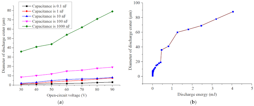
  • The larger the open-circuit voltage and capacitance, the larger the discharge energy, and thus there is more energy consumed in the formation of a discharge crater. The diameter of the discharge crater increases with capacitance and open-circuit voltage. The minimum diameter of the discharge crater is 0.85 µm when the discharge energy is 4.5 × 10⁻⁵ mJ, while the maximum diameter of the discharge crater is 79.1 µm when the discharge energy is 4.05 mJ.
  • Due to the high energy density of the discharge plasma when the dielectric is broken down, the depth of the discharge crater significantly increases with the capacitance and open-circuit voltage.
  • The increase of the discharge energy causes more materials to melt and vaporize, leading to the increase of the discharge crater volume. The minimum volume of the discharge crater is 0.03 µm3 when the discharge energy is 4.5 × 10⁻⁵ mJ, while the maximum volume of the discharge crater is 27,724 µm3 when the discharge energy is 4.05 mJ. This is consistent with the theoretical analysis. This study has reference value for the further application of micro-EDM in adopting deionized water as a dielectric.

Author Contributions

Conceptualization, Q.L. and T.N.; methodology, Z.C.; validation, Q.L. and Y.W.; formal analysis, D.J. and Y.W.; investigation, T.N. and Y.W.; resources, Q.L.; data curation, T.N. and Y.W.; writing—original draft preparation, T.N.; writing—review and editing, Q.L.; supervision, Q.L. and Z.C.; project administration, Q.L.; funding acquisition, Q.L. All authors have read and agreed to the published version of the manuscript.

Funding

Natural Science Foundation of Shandong, China (Grant No. ZR2019BEE037); Applied Basic Research Program of Qingdao (Grant No. 18-2-2-6-jch).

Data Availability Statement

Data is contained within the article.

Conflicts of Interest

The authors declare no conflict of interest.

References

  1. Rafa, W.; Dorota, O. Experimental investigation of surface layer properties of high thermal conductivity tool steel after electrical discharge machining. Metals 2017, 7, 550. [Google Scholar]
  2. Sabyrov, N.; Jahan, M.; Bilal, A.; Perveen, A. Ultrasonic vibration assisted electro-discharge machining (EDM)—An overview. Materials 2019, 12, 522. [Google Scholar] [CrossRef] [Green Version]
  3. Quarto, M.; Bissacco, G.; D’Urso, G. Study on ZrB2-based ceramics reinforced with SiC fibers or whiskers machined by micro-electrical discharge machining. Micromachines 2020, 11, 959. [Google Scholar] [CrossRef] [PubMed]
  4. Muthuramalingam, T. Effect of diluted dielectric medium on spark energy in green EDM process using TGRA approach. J. Clean. Prod. 2019, 238, 117894.1–117894.8. [Google Scholar] [CrossRef]
  5. Ray, A. Multi-objective optimization of green EDM: An integrated theory. J. Inst. Eng. 2014, 96, 41–47. [Google Scholar]
  6. Baroi, B.K.; Jagadish, T.D.; Patowari, P.K. Machinability assessment of titanium grade 2 alloy using deionized water in EDM. Mater. Today Proc. 2020, 26, 2221–2225. [Google Scholar] [CrossRef]
  7. Nguyen, M.D.; Rahman, M.; Wong, Y.S. An experimental study on micro-EDM in low-resistivity deionized water using short voltage pulses. Int. J. Adv. Manuf. Tech. 2012, 58, 533–544. [Google Scholar] [CrossRef]
  8. Chung, D.K.; Shin, H.S.; Kim, B.H.; Park, M.S.; Chu, C.N. Surface finishing of micro-edm holes using deionized water. J. Micromech. Microeng. 2009, 19, 045025. [Google Scholar] [CrossRef]
  9. Yu, Z.; Kunieda, M. Study on material removal rate of EDM in deionized water. Denki Kako Gakkaishi 2010, 33, 28–36. [Google Scholar] [CrossRef]
  10. Liu, Q.; Zhang, Q.; Zhang, M.; Zhang, J. Review of size effects in micro electrical discharge machining. Precis. Eng. 2016, 44, 29–40. [Google Scholar] [CrossRef]
  11. Liu, Q.; Zhang, Q.; Zhang, M.; Yang, F. Study on the discharge characteristics of single-pulse discharge in micro-EDM. Micromachines 2020, 11, 55. [Google Scholar] [CrossRef] [PubMed] [Green Version]
  12. Ablyaz, T.R.; Shlykov, E.S.; Muratov, K.R.; Mahajan, A.; Singh, G.; Devgan, S.; Sidhu, S.S. Surface characterization and tribological performance analysis of electric discharge machined duplex stainless steel. Micromachines 2020, 11, 926. [Google Scholar] [CrossRef] [PubMed]
  13. Quarto, M.; Bissacco, G.; D’Urso, G. Machinability and energy efficiency in micro-EDM milling of zirconium boride reinforced with silicon carbide fibers. Materials 2019, 12, 3920. [Google Scholar] [CrossRef] [PubMed] [Green Version]
  14. D’Urso, G.; Maccarini, G.; Quarto, M.; Ravasio, C.; Caldara, M. Micro-electro discharge machining drilling of stainless steel with copper electrode: The influence of process parameters and electrode size. Adv. Mech. Eng. 2016, 8, 1–16. [Google Scholar] [CrossRef] [Green Version]
  15. Zhu, Z.; Guo, D.; Xu, J.; Lin, J.; Lei, J.; Xu, B.; Wu, X.; Wang, X. processing characteristics of micro electrical discharge machining for surface modification of TiNi shape memory alloys using a TiC powder dielectric. Micromachines 2020, 11, 1018. [Google Scholar] [CrossRef] [PubMed]
  16. Wang, K.; Zhang, Q.; Zhu, G.; Liu, Q.; Huang, Y.; Zhang, J. Research on the energy distribution of micro EDM by utilization of electro-thermal model. Int. J. Adv. Manuf. Tech. 2017, 93, 4179–4186. [Google Scholar] [CrossRef]
  17. Panda, D.K.; Bhoi, R.K. Developing transient three dimensional thermal models for electro discharge machining of semi infinite and infinite solid. J. Mater. Process. Manuf. Sci. 2001, 10, 71–89. [Google Scholar] [CrossRef]
  18. D’Urso, G.; Maccarini, G.; Ravasio, C. Process performance of micro-EDM drilling of stainless steel. Int. J. Adv. Manuf. Tech. 2014, 72, 1287–1298. [Google Scholar] [CrossRef]
Figure 1. Diagrammatic sketch of the thermal conduction at discharge point.
Coatings 11 00322 g001
Figure 2. Schematic diagram of microelectrical discharge machining (micro-EDM) platform.
Coatings 11 00322 g002
Figure 3. Picture of the discharge crater (Open-circuit voltage U = 110 V and capacitance C = 1000 pF).
Coatings 11 00322 g003
Figure 4. Effect of open-circuit voltage (a) and discharge energy (b) on the diameter of the discharge crater.
Coatings 11 00322 g004
Figure 5. Effect of open-circuit voltage (a) and discharge energy (b) on the depth of the discharge crater.
Coatings 11 00322 g005
Figure 6. Effect of open-circuit voltage (a) and discharge energy (b) on discharge crater volume.
Coatings 11 00322 g006
Table 1. Main discharge parameters.
Machining ParameterValue
Open-circuit voltage (U/V)30, 40, 50, 60, 70, 80, 90
Capacitance (C/nF)0.1, 1, 10, 100, 1000
Current-limiting resistance (R/Ω)50
Publisher’s Note: MDPI stays neutral with regard to jurisdictional claims in published maps and institutional affiliations.

