
Statistical Analysis on the Structural Size of Simulated Thin Film Growth with Molecular Dynamics for Glancing Angle Incidence Deposition


Abstract
:
1. Introduction
2. Materials and Methods
3. Results
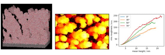
3.1. TiO2
3.2. SiO2
4. Discussion and Conclusions
Author Contributions
Funding
Institutional Review Board Statement
Informed Consent Statement
Data Availability Statement
Conflicts of Interest
References
- Turowski, M.; Jupé, M.; Melzig, T.; Moskovkin, P.; Daniel, A.; Pflug, A.; Lucas, S.; Ristau, D. Practice-oriented optical thin film growth simulation via multiple scale approach. Thin Solid Films 2015, 592, 240–247. [Google Scholar] [CrossRef]
- Turowski, M.; Jupé, M.; Ehlers, H.; Melzig, T.; Pflug, A. Simulation in thin film technology. In Optical Systems Design 2015: Advances in Optical Thin Films V; SPIE: Bellingham, WA, USA, 2015; Volume 9627, p. 962707. [Google Scholar] [CrossRef] [Green Version]
- Turowski, M.; Jupé, M.; Melzig, T.; Pflug, A.; Demircan, A.; Ristau, D. Multiple scale modeling of PVD sputter processes. Opt. Interf. Coat. 2016. [Google Scholar] [CrossRef]
- Grigoriev, F.; Sulimov, A.; Katkova, E.; Kochikov, I.; Kondakova, O.; Sulimov, V.; Tikhonravov, A. Full-atomistic nanoscale modeling of the ion beam sputtering deposition of SiO2 thin films. J. Non-Cryst. Solids 2016, 448, 1–5. [Google Scholar] [CrossRef]
- Steinecke, M.; Badorreck, H.; Jupé, M.; Willemsen, T.; Hao, L.; Jensen, L.; Ristau, D. Quantizing nanolaminates as versatile materials for optical interference coatings. Appl. Opt. 2020, 59, A236–A241. [Google Scholar] [CrossRef] [PubMed]
- Badorreck, H.; Steinecke, M.; Jensen, L.; Ristau, D.; Jupé, M.; Müller, J.; Tonneau, R.; Moskovkin, P.; Lucas, S.; Pflug, A.; et al. Correlation of structural and optical properties using virtual materials analysis. Opt. Express 2019, 27, 22209–22225. [Google Scholar] [CrossRef] [PubMed]
- Grineviciute, L.; Badorreck, H.; Jensen, L.; Ristau, D.; Jupé, M.; Selskis, A.; Tolenis, T. Impact of deposition conditions on nanostructured anisotropic silica thin films in multilayer interference coatings. Appl. Surf. Sci. 2021, in press. [Google Scholar]
- Grigoriev, F.V.; Sulimov, V.B.; Tikhonravov, A.V. Structure of highly porous silicon dioxide thin film: Results of atomis-tic simulation. Coatings 2019, 9, 568. [Google Scholar] [CrossRef] [Green Version]
- Matsui, M.; Akaogi, M. Molecular dynamics simulation of the structural and physical properties of the four polymorphs of TiO2. Mol. Simul. 1991, 6, 239–244. [Google Scholar] [CrossRef]
- Zhang, S.; Zhang, X.; Peng, H.; Wen, L.; Qiu, G.; Hu, M.; Bai, C. Structure analysis of CaO–SiO2–Al2O3–TiO2 slag by molecular dynamics simulation and FT-IR Spectroscopy. ISIJ Int. 2014, 54, 734–742. [Google Scholar] [CrossRef] [Green Version]
- Baskes, M.I.; Nelson, J.S.; Wright, A.F. Semiempirical modified embedded-atom potentials for silicon and germanium. Phys. Rev. B 1989, 40, 6085–6100. [Google Scholar] [CrossRef] [PubMed]
- Lee, E.; Lee, K.-R.; Baskes, M.I.; Lee, B.-J. A modified embedded-atom method interatomic potential for ionic systems:2NNMEAM+Qeq. Phys. Rev. B 2016, 93, 144110. [Google Scholar] [CrossRef] [Green Version]
- Buckingham, R.A.; Lennard-Jones, J.E. The classical equation of state of gaseous helium, neon and argon. Proc. R. Soc. Lond. Ser. A Math. Phys. Sci. 1938, 168, 264–283. [Google Scholar] [CrossRef]
- Plimpton, S. Fast parallel algorithms for short-range molecular dynamics. J. Comput. Phys. 1993, 117, 1–19. [Google Scholar] [CrossRef] [Green Version]
- Wolf, D.; Keblinski, P.; Phillpot, S.R.; Eggebrecht, J. Exact method for the simulation of Coulombic systems by spherically truncated, pairwise r−1 summation. J. Chem. Phys. 1999, 110, 8254–8282. [Google Scholar] [CrossRef]
- Rose, A.S.; Hildebrand, P.W. NGL Viewer: A web application for molecular visualization. Nucleic Acids Res. 2015, 43, W576–W579. [Google Scholar] [CrossRef] [PubMed]
- Rose, A.S.; Bradley, A.R.; Valasatava, Y.; Duarte, J.M.; Prlić, A.; Rose, P.W. Web-Based Molecular Graphics for Large Com-plexes. In Proceedings of the 21st International Conference on Web3D Technology, Anaheim, CA, USA, 22–24 July 2016. [Google Scholar] [CrossRef]
- Duparré, A.; Ferre-Borrull, J.; Gliech, S.; Notni, G.; Steinert, J.; Bennett, J.M. Surface characterization techniques for deter-mining the root-mean-square roughness and power spectral densities of optical components. Appl. Opt. 2002, 41, 154–171. [Google Scholar] [CrossRef] [PubMed] [Green Version]
- Welch, P. The use of fast Fourier transform for the estimation of power spectra: A method based on time averaging over short, modified periodograms. IEEE Trans. Audio Electroacoust. 1967, 15, 70–73. [Google Scholar] [CrossRef] [Green Version]
- Harris, C.R.; Millman, K.J.; van der Walt, S.J.; Gommers, R.; Virtanen, P.; Cournapeau, D.; Wieser, E.; Taylor, J.; Berg, S.; Smith, N.J.; et al. Array programming with NumPy. Nature 2020, 585, 357–362. [Google Scholar] [CrossRef] [PubMed]
- Virtanen, P.; Gommers, R.; Oliphant, T.E.; Haberland, M.; Reddy, T.; Cournapeau, D.; Burovski, E.; Peterson, P.; Weckesser, W.; Bright, J.; et al. SciPy 1.0: Fundamental algorithms for scientific computing in python. Nat. Methods 2020, 17, 261–272. [Google Scholar] [CrossRef] [PubMed] [Green Version]


| TiO2 | 7 × 8 nm2 | 30 × 20 nm2 | ||||||
|---|---|---|---|---|---|---|---|---|
| 0° | 30° | 50° | 70° | 0° | 30° | 50° | 70° | |
| Fill factor in % | 86.2 | 83.3 | 74.3 | 62.5 | 63.4 | 59.6 | 52.0 | 37.1 |
| 0.0036 | 0.0286 | 0.0429 | 0.0625 | 0.0050 | 0.0185 | 0.0074 | 0.0131 | |
| 7–20 nm2 | 0° | 30° | 50° | |||
| Fill factor in % | 46.6 | 47.37 ± 0.65 | 45.2 | 46.37 ± 0.83 | 44.8 | 44.77 ± 0.05 |
| 47.3 | 46.8 | 44.7 | ||||
| 48.2 | 47.1 | 44.8 | ||||
| 0.0123 | 0.0122 ± 0.0004 | 0.0129 | 0.0127 ± 0.0003 | 0.0137 | 0.0132 ± 0.0004 | |
| 0.0127 | 0.0123 | 0.0129 | ||||
| 0.0118 | 0.0128 | 0.0130 | ||||
| 25–47 nm2 | 0° | 30° | 50° | |||
| Fill factor in % | 63.3 | 64.03 ± 0.52 | 61.8 | 62.60 ± 0.65 | 62.0 | 59.80 ± 1.59 |
| 64.3 | 63.4 | 59.1 | ||||
| 64.5 | 62.6 | 58.3 | ||||
| 0.0041 | 0.0033 ± 0.0006 | 0.0046 | 0.0023 ± 0.0018 | 0.0020 | 0.0013 ± 0.0007 | |
| 0.0031 | 0.0021 | 0.0004 | ||||
| 0.0026 | 0.0002 | 0.0015 | ||||
Publisher’s Note: MDPI stays neutral with regard to jurisdictional claims in published maps and institutional affiliations. |
© 2021 by the authors. Licensee MDPI, Basel, Switzerland. This article is an open access article distributed under the terms and conditions of the Creative Commons Attribution (CC BY) license (https://creativecommons.org/licenses/by/4.0/).
Share and Cite
Badorreck, H.; Jensen, L.; Ristau, D.; Jupé, M. Statistical Analysis on the Structural Size of Simulated Thin Film Growth with Molecular Dynamics for Glancing Angle Incidence Deposition. Coatings 2021, 11, 469. https://doi.org/10.3390/coatings11040469
Badorreck H, Jensen L, Ristau D, Jupé M. Statistical Analysis on the Structural Size of Simulated Thin Film Growth with Molecular Dynamics for Glancing Angle Incidence Deposition. Coatings. 2021; 11(4):469. https://doi.org/10.3390/coatings11040469
Chicago/Turabian StyleBadorreck, Holger, Lars Jensen, Detlev Ristau, and Marco Jupé. 2021. "Statistical Analysis on the Structural Size of Simulated Thin Film Growth with Molecular Dynamics for Glancing Angle Incidence Deposition" Coatings 11, no. 4: 469. https://doi.org/10.3390/coatings11040469