1. Introduction
Anti-reflection thin film plays a vital role in anti-glare displays [
1], automobile dashboards [
2], solar cells [
3,
4,
5,
6] and most optical systems [
7,
8,
9,
10,
11]. By precisely controlling the refractive index and thickness of each film layer, depositing a coating having four or more layers on a substrate can generally reduce surface reflection to nearly zero over a wide range of wavelengths. Nowadays, based on optimizing interference phenomena in stacked systems, different mathematical algorithms are used to design multilayer optical coatings [
12]. The optical parameters of thin film, such as transmittance, reflectance, and absorption, can targets for design optimization [
13]. No simple or feasible method goes into the design of ultra-broadband anti-reflection coatings. It can only rely on numerical optimization technology to continuously optimize the initial design and even use automatic synthesis technology to generate a film structure that meets the design requirements. For the ultra-wideband, anti-reflection film in this article, there was no suitable initial structure of the multilayer film. During design optimization, the refractive index of the film material is usually fixed, and only the film’s thickness is used as the design parameter because the thickness of each layer in the final film structure is irregular. For the film structure of the ultra-broadband, anti-reflection film, the number of layers must be very large, and many extremely thin layers must exist. The ultra-wideband, anti-reflection characteristics achieved in the final plating process almost entirely depend on the control accuracy of the film thickness [
14]. There are many ways to control the thickness of optical coatings, including crystal vibration monitoring, and optical monitoring. For the film thickness control of the ultra-wideband anti-reflection film, no monitoring method is perfect because film thickness in the film structure varies greatly from a few nanometers to a few hundred nanometers [
15]. Therefore, there is an urgent need for an adjustable, low-cost, stable, and repeatable coating process for broadband antireflection coatings.
In addition to the optical waveband range, a main factor affecting the design and preparation of the antireflection coating is the incident angle range [
16]. Since the fundamental reason for the anti-reflection effect of the optical multilayer film is the light interference in the multilayer film structure, it is impossible to achieve an excellent anti-reflection effect through the multilayer film structure in the case of large incident angles [
17,
18]. At present, researchers usually use nanostructures to construct equivalent refractive index gradient structures to achieve wide-angle antireflection effects. However, to prepare a pure nanostructure antireflection structure with an excellent antireflection effect, the process is cumbersome and the cost is high. In addition, it is difficult to control the defective impurities in the process with numerous steps such as lithography, etching, and cleaning [
19].
Oblique-angle deposition (OAD) is a method of growing low-refractive-index porous films through surface diffusion and self-shading effects during the deposition process [
20,
21,
22,
23,
24]. Random growth fluctuations on the substrate will produce shadow areas that the incident steam flux cannot reach, and non-shadow areas where the incident light flux is preferentially deposited, thereby forming a directional rod-like structure with high porosity. This is defined as the angle between the normal and sample surfaces and the incident vapor flux, which results in the formation of a nanorod structure at an incline relative to the sample surface. Because the gap between nanorods can be much smaller than the wavelength of visible and infrared light, the nano-structured layer acts as a single homogeneous film with a refractive index between that of air and nanorod materials and increases as the porosity the refractive index decreases. SiO
2 coatings are known for their long-term stability and high transmittance in a wide spectral range. By convention, the refractive index of dense SiO
2 is about 1.46, while the refractive index of porous SiO
2 can be reduced to 1.1 or lower by increasing the porosity [
25,
26,
27].
Researchers had already used several thin film layers with different refractive indices prepared by the OAD method to construct a graded refractive index structure, which can achieve a relatively good antireflective property [
28,
29,
30]. However, the outermost layer is usually deposited at an angle greater than 75° in order to obtain a lower refractive index film layer close to that of air. The air inside such a film layer is relatively large, the film layer is particularly loose, and the built-up multilayer antireflection film has a poor bonding force, so it cannot meet the requirements of the general use environment of the optical system at all.
In this paper, we combined the OAD method with the Dual Ion Beam Sputter (DIBS) coating process, which can control film thickness with high precision. In this way, we greatly simplified the film structure, reduced coating difficulty, and improved process repeatability and stability while ensuring the anti-reflection performance of a wide band and wide incident-angle range. A broadband AR coating, applied in the wavelength range of 400–2000 nm, was designed and then deposited by IBS. Ta
2O
5 and SiO
2 were chosen as high- and low-refraction coating materials, respectively. Because of its extremely stable coating rate and high material reduction ability, DIBS deposition is preferred for ultra-broadband antireflection coatings [
31,
32]. By using a precise time-controlled deposition method, the film thickness error can be kept very low. At the same time, the outermost layer was replaced by obliquely deposited SiO
2. The parameters of the OAD preparation process were determined by measuring and calculating the refractive index of the SiO
2 layer deposited at different incident angles. The two optimized structures contain 22 and 36 layers, each having ultrathin layers and sensitive layers. The most critical factor to consider for obtaining high transmittance is the thickness uniformity of each thin and sensitive layer. A time monitoring strategy was successfully used to control the thickness of the layers during the deposition process.
2. Materials and Methods
In this study, broadband AR coatings were fabricated using the dual ion beam sputtering process. Because of the high energy of deposited particles during preparation, the films prepared by DIBS have excellent optical stability, environmental stability, and repeatability. The Veeco’s (New York, NY, USA) SPECTOR DIBS optical coating system is shown in
Figure 1a. Ta
2O
5 and SiO
2 were used as high- and low-refractive index coating materials, respectively. The deposition rate of the film material was determined by the sputtering power of the 16 cm RF ion source and the shielding ratio of the mask. The sputtering distribution of the film material depends on the incident angle of the ion beam relative to the target and the sputtering characteristics of the film material. In the process of thin-film deposition, O
2 should be supplied to the 12 cm auxiliary ion source to ensure the proper degree of oxidation for the film materials. The deposition rate of Ta
2O
5 was 0.23 Å/s, and the deposition rate of SiO
2 was 0.34 Å/s. The rate was very stable over 1–2 h of coating deposition process. Owing to its excellent stability, we used a precise time controlling method to prepare the multilayer AR coating. Precision-polished sapphire glasses with a size of 1 inch were used as the substrate material. The glasses have an extremely low surface roughness Ra, much lower than conventional glass materials. The surface roughness was measured by an interferometric optical profiler after native oxide removal and cleaning. Precision grade (Ra < 1 nm) roughness for optical grade substrates plays a key role in deposition since the substrate surface has a direct effect on the adhesion and agglomeration of the films deposited. The average surface roughness (Ra) was determined to be 0.343 nm as shown in
Figure 1b. The substrate clamping device used in the coating process is a high-speed rotating planetary fixture having a precisely tested and processed uniformity correction baffle. The thickness uniformity error of the film on the surface of the 1-inch substrate was better than ±0.1%. Therefore, the influence of the film’s lateral uniformity on its antireflection performance on the substrate surface can be ignored. Prior to deposition, the samples were cleaned in acetone and methanol, rinsed in de-ionized water, and subsequently dried in a stream of nitrogen gas. Then, they were fixed on a rotated plane fixture located in a position that faced the coating material target. The substrate temperature was heated and kept at 200 °C by a heater in the vacuum chamber during the entire deposition process. The obliquely deposited porous SiO
2 layer was prepared by changing the deposition angle (θ) between the plane and vapor source.
During the experiments, the refractive index, transmittance, and cross-sectional morphology of the thin films were evaluated using an ellipsometer (GES5E of Semilab, Budapest, Hungary), spectrophotometer (Lambda 1050 of PerkinElmer, Waltham, MA, USA), and scanning electron microscope (SEM, JSM-6510 of JEOL, Tokyo, Japan), respectively.
3. Results and Discussion
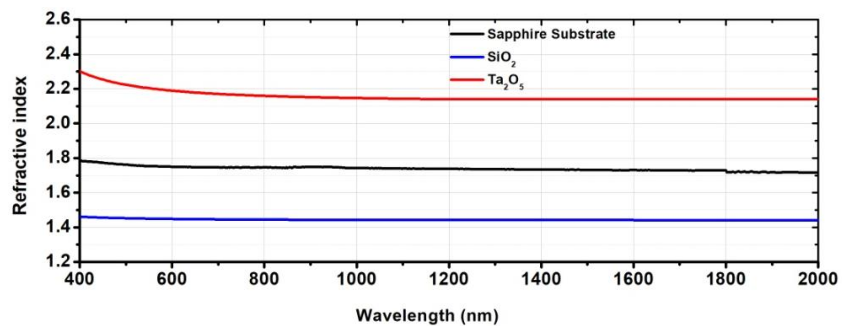
Essential Macleod software (version 10.6) was employed to design broadband AR coatings in the range of 400–2000 nm. The refractive indices of Ta
2O
5 and SiO
2 are shown in
Figure 2, which were calculated based on the measurement data of a single layer on a polished wafer using an ellipsometer. In the investigated band, the extinction coefficient k of the two coating materials prepared by the DIBS process was almost zero. For a uniform structure, the sputter deposition rate of the material should be kept relatively low. Thus, the deposition thickness per unit time can be reduced as much as possible, and the controlled accuracy can be improved, which is critical for the thickness control of extremely thin layers. Full-band material refractive index data were the basis of the film design.
The refractive index of the material was calculated by applying the measurement data of the ellipsometer. In the investigation band, data were collected in 1 nm intervals. The refractive index data were relatively sufficient for our calculations, which was the main reason for not using the spectral measurement calculation method to obtain the refractive index of coating materials. There was a large deviation in the refractive index of the coating material between short and long wavelengths. Sufficient refractive index data can improve the accuracy of film optimization, which is more critical for shortwave design. In the shorter band, the transmittance curve had more ripples, and a slight deviation of the refractive index caused the transmittance of some wavelengths to be much lower than average. According to the coating experiment, the thickness difference of the broadband AR thin film layers sis very large. In addition to accurately measuring the refractive index of the material, the thickness deviation correction of the film was also one of the key factors in improving the accuracy of the deposition.
Figure 3 shows the correspondence between design thickness and deposition thickness. The standard correspondence relationship should be one to one. However, there was another calculation error about film thickness which is a function of time. Because the shutter was switched on and off when changing layer during deposition, the film’s deposition was nonlinear, this is a significant error between the designed film thickness and the actual thickness. Furthermore, through multiple experiments, the error bar of film layers with different design thicknesses and an average value was obtained. In the subsequent multi-layer film design process, the thickness correction data obtained was employed to improve design accuracy.
Through the combination of various optimization algorithms, we obtained two relatively good design results: 22-layer and 36-layer AR coatings. The top layer of each film stack used a porous SiO
2 thin film with a refractive index of 1.28 The comprehensive decision to use an OAD film with this refractive index resulted from considering the design requirements and the firmness and durability of the actual film. The thickness distribution and refractive index changes of the two film stacks are shown in
Figure 4a,b. A comparison of the stacks showed that the 36-layer film structure contained more ultrathin layers (<10 nm), which is accordingly more difficult to manufacture.
Figure 4c shows the transmittance curves of the designed thin film stacks with and without the corresponding OAD film layer. All transmittance data were obtained from measurements on sapphire substrates coated with the same AR coatings on both sides. The 22-layer AR coating had an average transmittance of 98.5% from 400–2000 nm, while the 36-layer AR coating transmittance reached 99.2%. For most optical systems, this result was quite good.
Figure 5a,b shows the relative sensitivity of the two designed coating stacks. The film layers that had a significant influence on transmittance were second and fifth layers. Because the ultrathin layer has a greater thickness error rate, we coordinated the relationship between the sensitive and the ultrathin layers to obtain a design result with higher accuracy for the thickness control of the sensitive layer. In addition to adjusting the design of the sensitivity layer to improve manufacturing accuracy, a low-rate coating was actually used for the film layer having higher sensitivity [
33]. Correspondingly, the refractive index of the film layer with a reduced deposition rate was recalibrated by the ellipsometer, and the thickness error was corrected. When analyzing the relative sensitivity of the film, it was found that the thickness error of the top OAD film layer had little effect on transmittance, but the slight error of its refractive index had a significant impact on overall transmittance. Therefore, the preparation process of OAD needs detailed calculation and analysis to ensure that the refractive index of the porous SiO
2 is stable and accurate.
In order to obtain low refractive index film layers or porous thin film materials, a great deal of research was conducted using OAD. Generally, the relationship between φ and θ (
Figure 1) can be described by Tait’s rule [
34]:
Figure 6a shows both the measured and theoretical dependence of φ and θ according to Tait’s rule. When θ is less than 45°, the measured results conform accurately. However, as θ increases above 45°, its measured value becomes slightly larger than the theoretical value. Moreover, the increased φ leads to a discontinuous columnar structure with many more voids, which degrades the quality of prepared SiO
2 films. The refractive index of the SiO
2 film layer deposited at different angles was also measured by the ellipsometer, as shown in the right axis of
Figure 6a. For the SiO
2 with a refractive index of 1.28, the deposition angle should be controlled at 67°, as shown in
Figure 6b. The refractive index of the obliquely deposited SiO
2 is actually the effective refractive index
neff, which can be calculated by using Bruggeman’s effective medium approximation. The symmetrical, two-dimensional Bruggeman equation for two-material mixtures [
35] is expressed as
where
F is the areal-fraction of the SiO
2,
n0 is the refractive index of air, and
n1 is the refractive index of the nanostructure material SiO
2. For an equivalent refractive index of 1.28, the duty cycle F is equal to 64.15%.
Based on the determined process parameters, a highly accurate, multi-layer, anti-reflection film was prepared, as shown in
Figure 7a. The actual research process was based on a multi-layer film where there was no top OAD film layer. According to the film thickness correction and preparation process optimization introduced earlier, the transmittance of the prepared multi-layer film should be as close as possible to the theoretical design. Finally, with precise control of the rotation angle of the fixture and the deposition of the OAD film layer, we obtained samples of 22-layer and 36-layer AR coatings coated on both sides. The measured transmittance of the samples was 98.4 and 99.11% from 400–2000 nm, respectively. In addition, we analyzed the transmittance of the 36-layer AR coating sample with the incident angle. When the incident angle was below 47°, the transmittance could still be maintained above 98%, as shown in
Figure 7b.
Figure 8 shows the change of the sapphire transmission rate of the 36-layer AR coating coated on both sides as a function of the incident angle. It can be seen that when the incident angle was increased to 60°, it still had a certain anti-reflection effect, and the average transmittance could be maintained above 92%. In the case of oblique incidence, the difference in transmittance of P-polarized light and S-polarized light was not significant. When the light is incident on the surface of AR coating at 45°, the average transmittance of P-polarized light was 2.3% higher than that of S-polarized light.
Figure 9 shows the actual photos of AR coating samples. Compared with the empty sapphire substrate, the anti-reflection effect can be seen. We also tested the adhesion of the film on the sample surface. After being repeatedly pulled by tape CT-24, the broadband AR coating exhibited stable adhesion. Introducing the low-refractive index obliquely deposited SiO
2 layer can simplify the film system and improve coating precision without reducing environmental adaptability. We also conducted an environmental durability test. First, the sample was dried and heated at 80 °C for 2 h, then cooled to −20 °C for 2 h, and this step was cycled 20 times, and finally kept at 80 °C and 80% relative humidity for 72 h. By comparing the samples before and after durability test, there was no obvious difference in outlook and transmittance, as shown in
Figure 9.


 ,
, 