Article

Heterogeneous Bonding of PMMA and Double-Sided Polished Silicon Wafers through H2O Plasma Treatment for Microfluidic Devices

by
Chao-Ching Chiang
1,
Philip Nathaniel Immanuel
1,*,
Yi-Hsiung Chiu
2 and
Song-Jeng Huang
1,*
1
Department of Mechanical Engineering, National Taiwan University of Science and Technology, Taipei 106, Taiwan
2
Pacific Engineers & Constructors, Ltd. (PECL), Taipei 106, Taiwan
*
Authors to whom correspondence should be addressed.
Coatings 2021, 11(5), 580; https://doi.org/10.3390/coatings11050580
Submission received: 18 April 2021 / Revised: 11 May 2021 / Accepted: 14 May 2021 / Published: 17 May 2021

Abstract

:
In this work we report on a rapid, easy-to-operate, lossless, room temperature heterogeneous H2O plasma treatment process for the bonding of poly(methyl methacrylate) (PMMA) and double-sided polished (DSP) silicon substrates by for utilization in sandwich structured microfluidic devices. The heterogeneous bonding of the sandwich structure produced by the H2O plasma is analyzed, and the effect of heterogeneous bonding of free radicals and high charge electrons (e) in the formed plasma which causes a passivation phenomenon during the bonding process investigated. The PMMA and silicon surface treatments were performed at a constant radio frequency (RF) power and H2O flow rate. Changing plasma treatment time and powers for both processes were investigated during the experiments. The gas flow rate was controlled to cause ionization of plasma and the dissociation of water vapor from hydrogen (H) atoms and hydroxyl (OH) bonds, as confirmed by optical emission spectroscopy (OES). The OES results show the relative intensity peaks emitted by the OH radicals, H and oxygen (O). The free energy is proportional to the plasma treatment power and gas flow rate with H bonds forming between the adsorbed H2O and OH groups. The gas density generated saturated bonds at the interface, and the discharge energy that strengthened the OH-e bonds. This method provides an ideal heterogeneous bonding technique which can be used to manufacture new types of microfluidic devices.

1. Introduction

PMMA is a common material often used to fabricate microfluidic devices/chips, due to its good optic transparency, chemical properties, high thermal stability, low price, and biocompatibility [1]. This transparent polymer is available commercially in pellet, small granule, and sheet forms, which can be easily processed by thermoplastic methods (including injection molding, compression molding, and extrusion) for the production of microfluidic devices and low-cost disposable devices for biological applications. Polymers are very good materials for microdevice engineering and its applications because they are easy to fabricate and have high optical transparency and good strength to weight ratio [2]. Polymer materials with low molecular weights and repeated units can be fabricated using a variety of physical processes and chemical etching techniques, such as coining, photolithography, electrochemical etching [3,4], and pressure-based low/room temperature bonding [5]. Different polymer materials have different antibacterial and optical properties which make them suitable for diverse applications in the medical testing field.
Silicon is a very important material in the semiconductor industry, [6] commonly used for the fabrication of complex integrated circuits [7], solar cells [8], image controllers [9], sensors [10,11], and microfluidic devices [12,13]. Over the past decade, regular plasma wafer bonding at room temperature has attracted a great deal of attention [14,15,16]. The bonded interfaces produced by such processes exhibit high surface energies and strengths which are equivalent to those obtained by using an annealing process in the range of 800−1000 °C before bonding by conventional wet chemical activation [17]. A plasma-based bonding method called sequential plasma-activated bonding (SPAB) [18] has been demonstrated which can be applied to bond biological microelectromechanical systems (BioMEMS) and microchannel devices for biological detection applications [19,20,21]. In SPAB, the formation of chemical bonds on the surface of the material causes spontaneous bonding and simultaneous removal of surface contaminants and native oxides. However, for temperature sensitive materials, and for bonding between materials with different thermal expansion coefficients, a low temperature bonding process is essential. The plasma activates the chemical (OH) bonds on the surface of the material and increases the surface energy. This process provides a high reactive chemical energy on the surface that allows spontaneous bonding at room temperature [22] which can be applied in the process of heterogeneous bonding to produce a non-destructive and better bonding technology. PMMA [23,24] and polydimethylsiloxane (PDMS) [25,26] are extensively used for the fabrication of microfluidic devices for the detection of biological information and as biosensor substrates. PMMA and PDMS are low toxic, chemically inert, easy to fabricate, rich gas permeable, and they have high optical transparency and good biocompatibility [27,28]. Microfluidic substrates require only a small amount of biological sample and small volume of reagent for effective, accurate, and high-speed analysis. These properties make this polymer particularly adapted for the fabrication of microdevices for separation and analysis of blood components. Accurate data can be obtained from a single-time measurement without issues of cross-contamination. PDMS and PMMA are appropriate for high pressure operations, but one of the most challenging issues in the process for the fabrication of a heterogeneous material is in bonding a completely structured microfluidic substrate with another flat substrate to form effectively sealed microchannels and without deformation [29].
A thin PMMA sealing layer may also be needed during the fabrication of microfluidic devices. The high light transmittance of PMMA, being optically transparent from 300 nm down to 700 nm, make it suitable for photoluminescence (PL) and Raman spectrometer detection [30,31]. The bonding quality of the PMMA layer in microfluidic applications is critical. Without a good seal, fluid leakage will certainly occur if there is breakage in the bonding at the interface layer. Moreover, all connection points must be sealed after bonding to prevent the liquid flowing through the channel from leaking. However, bonding methods for heterogeneous material devices are often difficult; they require a cleanroom to ensure a clean surface for the substrate. In addition, because of differences in the material characteristics, bending or breakage is easy. Surface cleaning and activation are required for silicon and polymer substrates. Numerous types of bonding techniques for the fabrication of heterogeneous substrates have been explored in past studies, such as thermal bonding [32], solvent bonding [33], plasma bonding [34], and laser welding [35,36]. An ideal lossless bonding process would produce a smooth interface, not deform the structure of the heterogeneous material, and the bond strength should be high. Thermal and microwave bonding methods are traditionally used for the fabrication of such bonds for microfluidic devices. However, they are not suitable for a heterogeneous bonding process, leading to an uneven interface and ruptures produce by stress concentration or uneven energy pulling between the chemical bonds (OH) [37]. In recent years, the easiest and fastest heterogeneous bonding technique has been found to be solvent bonding [38]. It is a lossless and high-quality technology for the permanent bonding of different materials. At the interface, because the surface tension affects the solvent and forms a uniform filmy layer, ensuring that the stress distribution is homogeneous. However, bubbles or residual solvent present at the bonding interface may lead to cracks. Furthermore, the chemical properties of the solvents pose a danger of pollution to the environment as they may deteriorate over time. Thus, solvent toxicity and its possible impact on experimenter safety need to be considered.
Many kinds of plasma treatment have been developed to facilitate the effective bonding of silicon wafers to PMMA, PDMS and glass [39,40,41,42]. Plasmas can enhance adhesiveness by removing surface contaminants and the oxide layer from the materials, producing rougher bonding surfaces [43] and more reactive chemical groups [44,45]. In particular, the OH + e bond units in PMMA can be converted to the H−C−H group, thereby changing the PMMA’s surface chemistry from hydrophobic to hydrophilic and increasing the surface roughness. All atoms in the functional groups are linked to OH bonds on the PMMA surface and to the rest of the molecules by covalent bonds, leading to an increase in roughness values. However, currently, no reports exist detailing the optimum bonding conditions of polymers to silicon-based substrates. Another advantage is that thermal effects and stress concentration problems can be avoided by using plasma processing surface activation for room temperature bonding. No heating is required.
In this study, we used a deep reactive-ion etching (DRIE) process, as well as a lithographic process and laser cutting for the formation of microchannels in the PMMA and DSP silicon wafers in combination with an H2O plasma activated bonding. The surface-treated PMMA substrates were cleaned using acetone (95%) and DI water (1:50) to remove any oil or grease. The substrates were then dipped in alcohol (95%) for 20 s to remove any native or residual contamination after which the silicon surface was cleaned by a Piranha solution sulfuric peroxide mix (SPM) and RCA-1 (Radio Corporation of America) and (RCA)-2 boiled solutions. Then the sample was dipped into dilute hydrofluoric acid (DHF; 1:200) for several seconds to remove any native surface oxide and any residual contamination from the solutions.
The H2O plasma treatment acts to break the chemical bonds on the polymer and silicon surfaces, separating the original molecular bonds. A plasma treatment process, using water vapor as the processing gas, can enhance network covalent bonding on the surface by the interfacial diffusion of covalent bonding. The water vapor generates reactive oxygen species, and hydroxyl radicals which allow covalent bonding at the interface [44,46]. The aim of this study is to describe the mechanism for plasma activation during surface activation of heterogeneous bonding. Plasma treatment of the PMMA and silicon surface increases the total surface energy, gas flow rate, and bonding strength. The polar groups including OH, C=O, and C–H [47,48,49] are linked to the driving forces for the speculated structure of the covalent bonds needed to achieve a lossless heterogeneous bonding process. This is a breakthrough in heterogeneous bonding technology.

2. Experimental Procedure

2.1. Fabrication of PMMA Microchannels and Bonding with Silicon Substrates through H2O Plasma

First, we used eight-inch silicon wafers for photolithographic processing. Photolithography transfer the pattern engraved on the mask to photosensitive chemical photoresist on the substrate. Here, a boron (B)-doped p-type single crystal-DSP silicon wafer (100) with a resistivity ranging from 1 to 10 Ω/cm (B = (1.34–14.6) × 1015/cm3) was used. The mono-Si surface was first cleaned by Piranha solution in SPM clean and then with RCA-1 (NH4OH:H2O2:H2O = 1:1:5 for 180 s) and RCA-2 (HC1:H2O2:H2O = 1:1:6 cleaned for 300 s) boiled solutions. Chemical treatment was carried out to etch the exposure pattern into the material. Then the photomask pattern was placed on the silicon substrate to form the Si-based microchannels. After etching, a laser cutting machine was used (Disco–DFL7160, DISCO, Tokyo, Japan) to cut samples to the required dimensions. The silicon was cut into 34 × 34 mm2 pieces for preparation of the microfluidic devices (34 × 34 mm2 pieces were cut from one eight-inch silicon wafer for preparation of microchannels on the DSP silicon-based wafer). Finally, the native surface oxide and residual contaminants from the solutions was removed by dipped into DHF for 5 s, and dried with N2, to be stored in a filtration and vacuum desiccator (model.550, kartell®, Noviglio, Italy).
The second process involves the fabrication and binding of the PMMA. The microchannel patterns were formed by hot pressing. The silicon was cut into 34 × 34 mm2 pieces for pattern molding. A mold was hot pressed onto the PMMA during the hot embossing process for the formation of microchannels. The microchannel pattern was transferred from a silicon substrate coated with No. AZ4999 positive photoresist (MicroChemicals GmbH, Ulm, Germany) by DRIE (RIE-400iPB, SAMCO, Kyoto, Japan). The microchannel pattern was transferred onto the surface of the silicon substrate. The etched silicon substrate was used as the first channel mold to make the second PMMA model (SHINKOLITE™ DX, Mitsubishi Chemical, Tokyo, Japan) during hot embossing of both substrate plates. A silicon strip was used to gradually emboss features into the PMMA, with a pressure of 1.5 MPa for 15 min through a jig. Upon completion of the holding time, the PMMA was cooled down and separated from the silicon mold at room temperature. This embossing produce the desired microchannel shape embedded in the PMMA. Then N2 was used to dry the sample and stored in a filtration and vacuum desiccator.
In this study, DSP silicon wafer microchannel sheets with a thickness of 540 μm and PMMA microchannel sheet with a thickness of 1.5 mm were used as samples. The samples were cleaned by ultra-sonication in a mixed solution of 99.5% DI water and ethanol (5:1 volume ratio mixture) for 5 min before being dried. Then, each sample was placed in cooled water powered by a cathode electrode. The plasma treatment was carried out using 99.5% water vapor in a flat-type H2O plasma cleaning chamber (Aqua Plasma, AQ-2000, Kyoto, Japan). The plasma reactor was operated at a radio frequency (RF) of 13.56 MHz. The chamber temperature was monitored by a resistive sensor that was connected to the sample surface and to an accurate temperature controller (temperature uniformity was less than ±0.5 °C). The H2O plasma pressure was kept at 2 kg/cm2, and the processing time was increased to 30, 60, 90, 120 and 300 s with a constant pressure. Different water vapor flow rates (30, 50, 60, 90 and 120 sccm) were used at nearly room temperature and with different applied powers (30, 60, 90 and 120 W), as shown in Figure 1.

2.2. Tensile Testing of Bond Strength

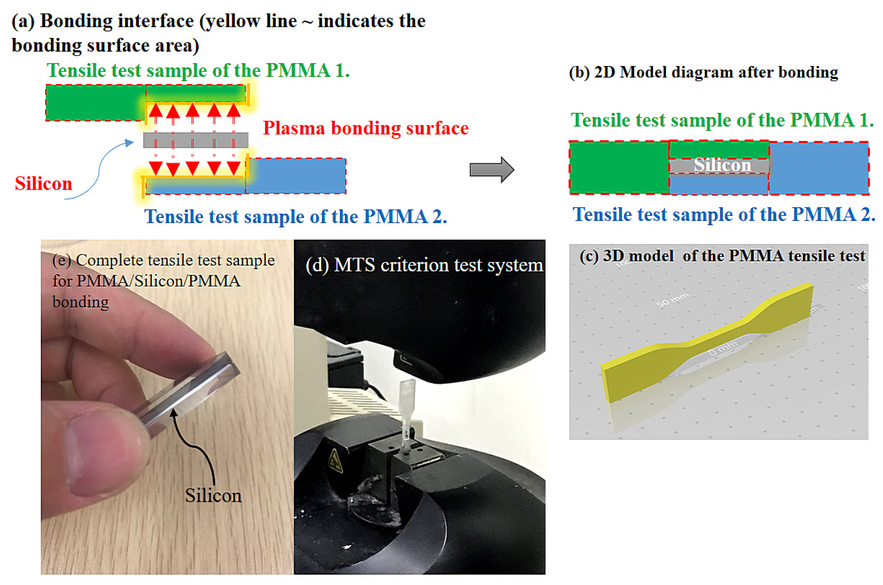
Prior to the tensile tests, each sample surface was cleaned by ultrasonication (Prema, DC80-900/H, Taichung, Taiwan) with acetone (95%) and DI water (1:50) for 30 s to remove any oil or grease from the surface. The samples were then dipped in alcohol (95%) for 30 s, dried in N2 gas, and stored in a desiccator. To prevent environmental contamination, the shelf life of the sample should not exceed 3 h. For every device, two strips of PMMA and a strip of silicon were bonded using an overlapping bond to form a sandwich type substrate prior to conducting lap tensile test (ASTM D638 [50], type V), as shown in Figure 2a,b. In total, 30 samples were tested using the lap tensile test method. The same procedure was followed in the experiments. The bond strength and quality of the devices were tested to find the best parameters for bonding the samples, including the H2O plasma parameters. The microfluidic device test model sample size before (PMMA/silicon/PMMA) bonding was as follows: width (9.53 mm), length (36.52 mm), overlapped area (19.94 mm × 3.2 mm), and grip area (12.4 mm × 3.2 mm). The microfluidic device sample size after bonding was as follows: width (9.53 mm) and length (63.5 mm), as shown in Figure 2c. An electromechanical test system MTS (Material Test System) Co., Ltd., Model C43, Eden Prairie, MI, USA) was used for the tensile tests. The tensile test data parameters were as follows: load cell: max 10 kN; pneumatic grip controller: 20 psi. The bonded samples were subjected to tensile testing to define the load at failure. The load cell speed was set to 1.0 mm/min. The loading cycle process showed that the tensile strength increased with the deformation of the sample until fracturing, at which time the force suddenly dropped to zero, as shown in Figure 2d. The main objective of the testing was to find the optimal bonding parameters, which would increase the surface energy of the interface and improve the bond strength. The H2O plasma treatment test results were considered for optimization of the bonding process. The heterogeneous sample produced by H2O plasma bonding for the tensile tests is shown in Figure 2e.

2.3. Optical Emission Spectroscopy

Optical emission spectroscopy (OES) (New ICP-OES PlasmaQuant 9100, Jena, Germany) was employed to monitor the effects of the reactive surface plasma treatment on the sample. As mentioned above, an H2O plasma treatment was used, and the effects on the material’s surface for changing plasma treatment times, powers and H2O plasma jet gas flows were investigated. The surface treatment of the material was performed with a constant voltage, to ensure that the water vapor plasma simultaneously reached a steady state in the plasma phase for all samples. OES was used to observe the radicals on the material surface after the plasma emission at wavelengths ranging from 200 to 1000 nm.

2.4. UV–Visible Transmission Spectrum

The PMMA commonly used for substrates in microfluidic device manufacturing is a notch sensitive thermoplastic material [51]. In biometric screening applications, such as for blood tests, it is important that the polymer should have excellent transmittance, even after plasma treatment. The pristine PMMA sample exhibited high transmission in the visible region of the spectrum above 300 nm, about 94% or higher. The optical absorption of PMMA is very small, less than 250−300 nm, and it exhibits higher transmission in the visible wavelength range [52,53]. The substrate produced using the plasma treatment did not differ much from the non-plasma treated samples, having had excellent interfacial adhesion together with excellent light transmittance efficiency. The microchannels retained good optical transmittance properties in the visible light region, which is a good foundation for blood testing. UV–visible spectroscopy (ACTTR, Type: UV1800, New Taipei, Taiwan) was used for detection in the experiments.

2.5. Interface Surface Analysis

The fabricated PMMA with H2O plasma treated surface was examined using an atomic force microscope (AFM) (Innova®, Bruker, Billerica, MA, USA) operated in core imaging mode—tapping-mode with a silicon tip. Bond strength and standard deviation for three samples were calculated to determine the best processing condition. The samples were dried in nitrogen gas. After bonding, changes in surface roughness of the samples were investigated by AFM. Observations of the samples after a 5-min plasma treatment and the untreated samples were made. Compared with the untreated samples, the plasma treated samples showed less roughness on the surface. The morphology of the bonded surfaces and interface was analyzed using field emission scanning electron microscopy (FE- SEM), (JEOL JSM-7000F, Tokyo, Japan), and automated optical inspection (AOI) (SQ3000, CyberOptics Corporation in Minneapolis, Minneapolis, MI, USA). The same devices were also used for automated visual inspection of the defect area of the microfluidic device and morphology of the microchannels after plasma treatment for all investigated samples. A cross-section of the bonding interface of the plasma treated sample was examined by high-resolution transmission electron microscopy (HR-TEM), ((JEOL) Japan Electron Optics Laboratory, JEM-2100, Tokyo, Japan) to obtain the diffraction pattern image. Nanoscale investigation of cross-sections of the PMMA and silicon bonded interface of the microchannel device was carried out. Observations showed the state of the interface after bonding at room temperature to be defect-free and tightly bonded. We achieved non-destructive heterogeneous bonding.

3. Results and Discussion

3.1. Chemical Energy Analysis by Optical Emission Spectroscopy (OES)

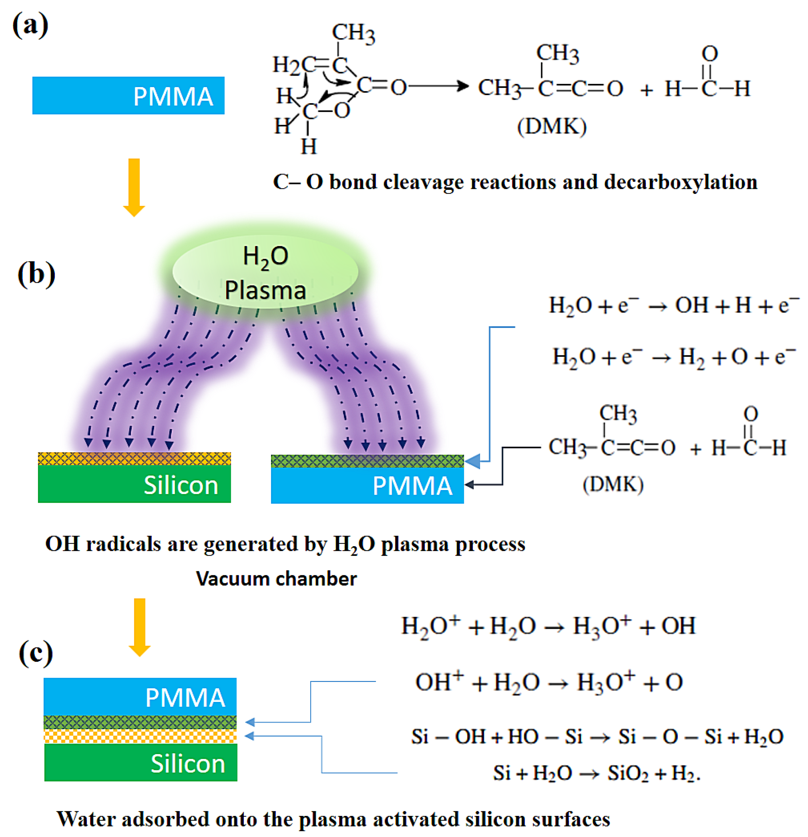
The chemical nature of PMMA (C5O2H8)n allows the preparation of microchannel patterns by hot pressing, softening, or melting upon heating; see Figure 3a. Propyl radicals occur during the reactions for the formation of dimethyl ketene (DMK) and formaldehyde [48]. Decarboxylation is a chemical process for the dissociation of carboxylic acids and esters by plasma [44,54], referring to the removal of a carbon atom from a carbon chain. The C=O bond decomposition reaction is the formation mechanism for formaldehyde and DMK. The major methyl methacrylate (MMA) fragmentation reactions occur in the plasma. The propyl radicals are considered as the predominant radical species. Decarboxylation of MMA yields a number of radicals, H−C and CO [54].
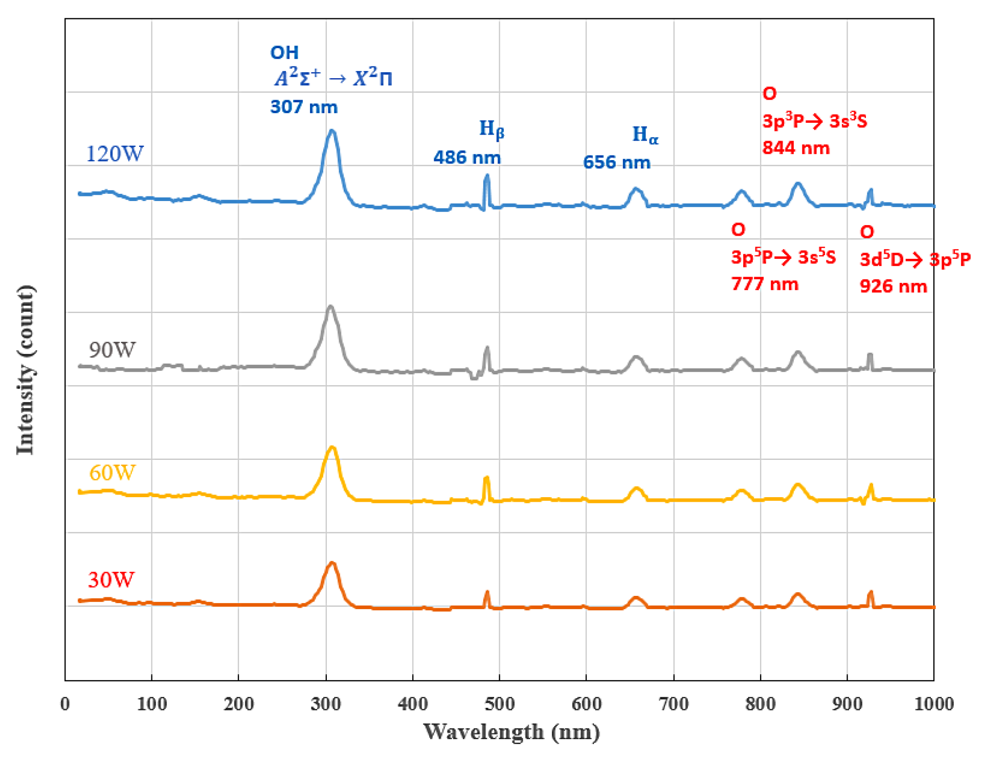
The RF method was used (13.56 MHz) with different powers (30, 60, 90 and 120 W), and different H2O plasma bonding times (30, 60, 90, 120 and 300 s). If the plasma time and water vapor (H2O) flow rate are excessively long, it can result in microchannel deformation or broken bonds at the interface. In addition, residual stresses can be produced during this bonding process when high plasma powers are used. If the linkage strength between the OH bonds and the substrate surface after air cooling is insufficient, or deformation occurs after heterogeneous bonding, it can cause fracturing of the silicon-based microchannels. That is attributed to the confinement of C=O and O−H of the PMMA chains within the molecular links, which can prevent segmental motion of the polymer chains. When the plasma activation temperature is controlled below 40 °C [44], there will be good polymer chain linkage. This suggests that the PMMA demonstrates better thermal stability at low temperatures. We also investigated the integrity of the bonding interface after the heterogeneous bonding process. The surface energy of mutual bonding of the OH bonds could be increased by controlling the gas flow and plasma processing time. One of the factors influencing the bonding is the heterogeneous bonding of the O bonds on the PMMA surface and Si−O bonds on the silicon. It is known that O−H2 aligns strongly with H2−SiO2 to bond substances. The surface energy of groups bonded by hydrogen bonding is strong [39]. For example, the bonding of hydrogen with organic molecules H2 + O + e on the PMMA surface, as shown in Figure 3b. The decomposition of MMA in the presence of oxygen was also investigated [55]. The products of the decomposition of the MMA monomer in H2O plasma are found to be CH3−C, H−O and O=C. The experimental results, together with the principles of chemistry, confirm the main process for the decomposition of MMA in an oxygen containing atmosphere. Plasma ionization and dissociation of water vapor on the PMMA surface bond hydrogen atoms and OH. These reactions are known to generate radicals due to the discharge of the OH + e bonds [29,53]. However, the surface energy of the OH bond is very strong, and this is one of the factors influencing the bonding of the silicon silanol groups Si−OH to the silicon surface. Surface activation by H2O plasma, together with the attractive interaction (hydrogen bonds) between the surface OH groups and water molecules, results in strong bonding. Irregular network structure of H and O bonds on the PMMA was formed by high energy from plasm, which breaks up the network structure of the bonds on the surface. Plasma ionization and dissociation of the water vapor bonds H atoms and OH. During surface activation at room temperature, the interfacial water enters the surrounding silicon interface layers causing the deformation of surface asperities. The PMMA surface is hydrophilized by the decomposition of organic molecules with the plasma to expose the hydrogen bonds, as confirmed by the AFM images [56]. At the same time, Si−O exists as a modified cation that can move freely at the interface (as O bonds) and is linked with the charge of the bridging oxygen. In particular, the OH groups from the silicon wafer surface move closer. Once the OH groups are sufficiently close, it is easier for links between molecules to produce covalent Si−O−Si bonds between the two interface surfaces (polymerization reaction), with water as a reaction product, as shown in Figure 3c. A strong linkage is produced owing to the OH–OH bonds. When the PMMA surface makes contact with OH + H2O, it is replaced by H3O+ + O. The reaction is shown in Equation (4) [57]. O + e exists as a modified surface energy that can move freely on the surface through the O bonds and linkages to supply the charge needed for the bridging H2. The water vapor plasma treatment transforms the positively charged H3O+ bonds. The effects on the PMMA and silicon surface of the H2O plasma treatment used in this study for different plasma treatment times, gas flows and plasma powers were investigated. The surface treatment on microchannel was done with constant voltage. An OES was observed to detect the radicals on the microchannel surface after the emission of plasma. The emission of O, H, and OH radicals was observed. There was an increase in the surface free energy with the plasma power. It is interesting that changes in intensity occurred. For a related study about the production of negative electrons (e) by the ionization and dissociation effects of plasma and OH radicals, please see [45]. Here, we demonstrated the discharge of the H2O plasma by introducing water vapor into the process chamber. OES analysis was used to characterize the H2O plasma treated sample. The effect of plasma surface modification was greater than the effect of oxidization due to the environmental impact. The results are shown in Figure 4. In H2O reactions, some ion collision occurs. Some examples are shown in Equations (1) and (3).
H 2 O + e     OH   +   H   +   e
H 2 O + e     H 2   +   O   +   e
H 2 O + + H 2 O     H 3 O +   +   OH
OH +   +   H 2 O     H 3 O +   +   O
Si OH + HO Si     Si O Si + H 2 O
Si + H 2 O     Si O 2   +   H 2
Plasma exposure directly affects the silicon surface, with bombardment causing changes to the surface structure of the silicon material. The H2O plasma treatment process enhance the chemical reactions at the silicon surface due to oxidization. The use of H2O plasma results in the formation of bonded interfaces with high surface energies. The oxidation produced by the chemical reaction is not the most critical factor in this bonding process [44,45]. The most important effect of plasma exposure seems to be the formation of a disordered surface structure producing Si−O−Si bonds and the generation of H3O+ + O on the PMMA surface leading to a chain reaction, for examples see Equations (4) and (5). Increased OH radicals driven by a strong electric field could be responsible for the removal of the oxide layer [44,53]. There is evidence of large charge electrons (e) in the plasma oxide formed after H2O plasma exposure. We call this oxidation process a passivation phenomenon in our experiments. The interfaces are bonded to each other with H bonds between the adsorbed H2O and OH groups. A higher plasma treatment energy is associated with changes in the Si–O–Si bonds, with shifting in the surface because of the growth of the Si–OH + HO–Si bonds at the bonding interface. This proves that a stronger bonding network forms with increased gas flow during the plasma treatment, achieving a high surface energy [58]. The high bond strength achieved after bonding at room temperature can be explained as due to an increase in the number of OH–OH bonds at the bonded interface, allowing for the formation of covalent bonds. The surface energy increases caused by the formation of Si–O–Si bonds linked to the oxygen to produce active intermediate H2O–OH+ bonds, following the reaction shown in Equation (6).

3.2. Bond Strength and Bonding Mechanism

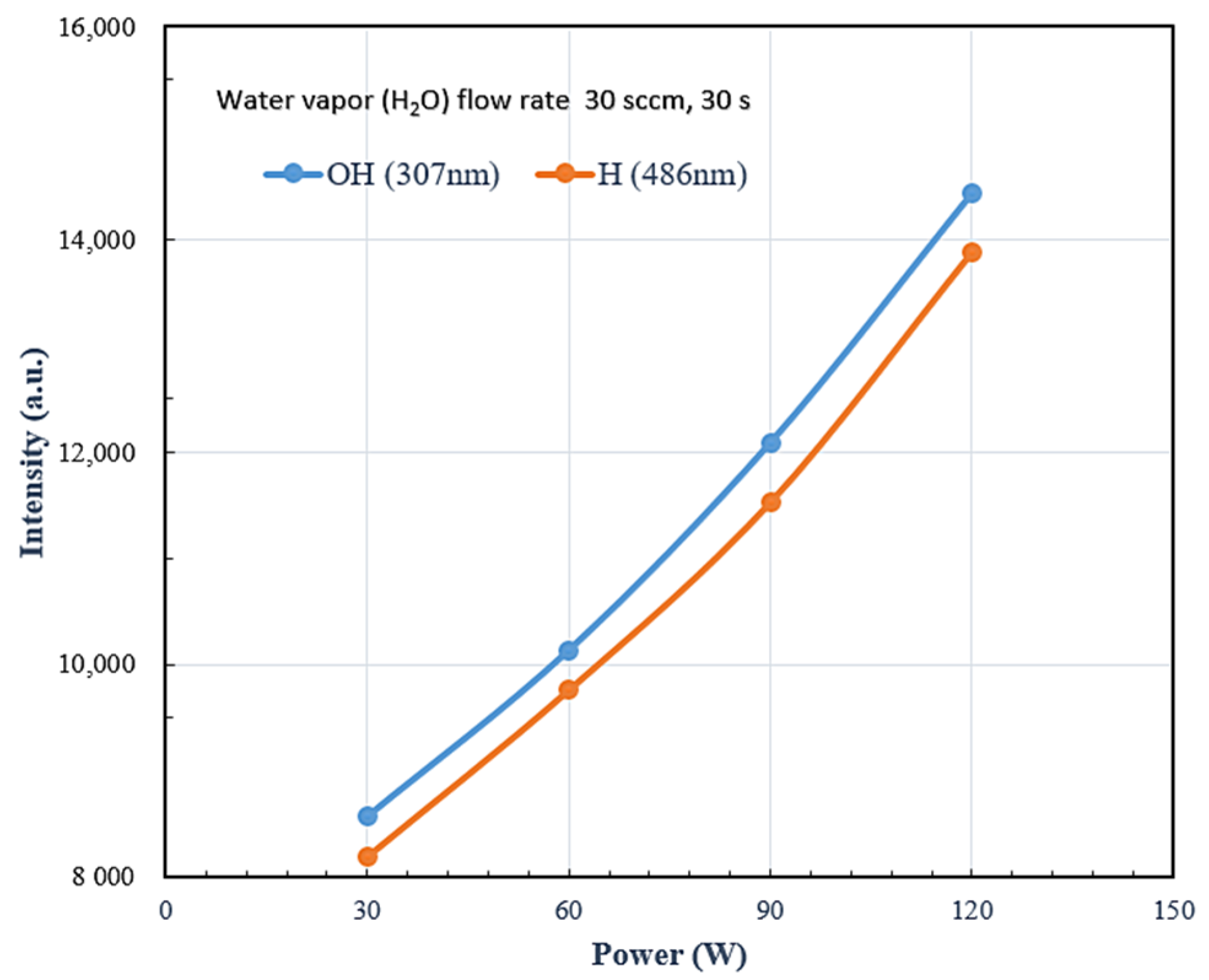
It has been proven that a higher plasma processing power can effectively increase the chemical reactions at the bonding interface, affecting the OH bonds. This increase is proportional to the length of the plasma treatment time, as confirmed by OES analysis conducted to characterize the effects of H2O plasma on the sample. The results show that the Si−O−Si bonds produced by the silicon and the HO+ + O generated on the PMMA surface together produce a strong chain reaction. The strong OES peaks detected for the OH bonds (307 nm) and H bonds (486 nm) both have a significant upward trend, as shown in Figure 5. From these results, it can be seen that the highest bond strength was achieved at 1.7 and 2.43 N/mm2 (that is three-fold higher than that of short-time bonding) at RF powers (13.56 MHz) of 60 and 120 W for 30 s, and H2O flow rate of 30 sccm, as shown in Table 1. The enhancement caused by the activation of the contact O=C bonds on the PMMA surface with changes in the Si–O–Si bonds. The shift on the silicon surface is because of the growth of Si–OH + HO–Si bonds at the bonding interface with covalence creating mutual bonding between them. Strength of the bond was increased after particle collisions during the H2O plasma process. The bonding strength was due to the production of OH−HO bonds. The positively charged O produces an enhancement effect. A total of 15 sets of parameters (including different gas flow rates and plasma processing times) were used in this work. Reducing the plasma gas flow rate below 30 sccm could produce weaker bonding strength or even fail. The energy produced on the surface of the specimen is too low, either because the energy between the covalent bonds is less or the amount is less. The experimental results show a reduction in the bonding strength for both plasma-treated samples when the gas flow rate was less than or greater than 60 sccm. We conclude, based on these results, that the shortest time required for plasma treatment is 30 s, and the most suitable parameters for bonding are a gas flow rate of 60 sccm and plasma power of 120 W.
After H2O plasma processing, the bond strength of the microfluidic sample at 60 W and flow rate 30 sccm was small, 1.7 N/mm2. The bond strengths for plasma processing flow rates from 30 sccm to 120 sccm had an approximate average value of 1.268 N/mm2 at normal circumstances. Table 1 shows the values for direct bonding for a plasma processing time of 120 s, with a maximum bond strength of 2.43 N/mm2 and utilizing an H2O plasma processing power of 120 W and gas flow rate from 60 sccm to 120 sccm for surface treatment. The bond strength was higher than that produced when the processing power was 60 W, an enhancement of 10%. The results verify the relationship between the bond strength and the fabrication process. The oxygen reacted with PMMA and produces active intermediates HO–C–OH, which were then dehydrated to produce formaldehyde and methyl pyruvate, [45] and the methyl pyruvate decomposed to generate acetone. This happened because of decomposition of the ester groups. By using a high plasma power to treat the surface of the silicon, we can achieve OH bonding through a splitting reaction between the methyl and the oxygen. The gas flow rate in this method causes the high O=C bonding activity. The Si−O−Si covalent bonds that form on the silicon surface enhance the bond strength between the two surfaces. Controlling the gas flow rate of the plasma is very important for microfluidic bonding.
The intensity of the 844.6 nm and 926 nm emission lines as a function of the gas flow rate is plotted in Figure 6a. It is assumed that more O bonds on the surface of the heterogeneously bonded samples after plasma treatment produces better bonding reactions between the O bonds and Si−O−Si + H2O. The 844.6 nm oxygen emission line has a higher intensity, so indicates increased reliability during the hetero-bonding process. The intensities of the 844.6 nm and 926 nm O emission lines are shown in Figure 6a. In the tests, increasing the gas flow rate cause a small decrease in the density of the atomic oxygen ions. This is attributed to the recombination of the O bond of active species on the surface of the substrate. In addition, increasing the gas flow rate from 30 to 60 sccm increases the intensity of the O emission lines, from 844 nm and 926 nm to 14,820 and 15,374, respectively, most likely due to recombination of O molecules with free electrons and the production of e + H2 ions; see Equation (7).
This phenomenon leads to a further decrease in the intensity of the oxygen atom emission line over 60 sccm. Increasing the gas flow rate from 60 to 120 sccm reduces the O emission intensity lines from 844 nm and 926 nm to 13,385 and 13,214, respectively. A higher plasma power rate leads to the production of more active radicals and ions on the surface, which in turn generates covalent bonds. When the samples are exposed to water vapor plasma, more water molecules cover the surfaces, until reaching a state of equilibrium. An increase in the silanol (Si−OH) density on the silicon surface also improves the bonding strength. Consequently, by controlling the gas flow rate, the bonding strength can be significantly improved and the active radicals reach saturation. The analytical result confirm that the O bonds are more active leading to stronger bonding forces. In contrast, the number of active radicals decreases after the chamber reaches saturation.
Si O Si + H 2 O + e     Si HO OH Si   +   e
We evaluated the bond strength in relation to the plasma treatment power (60 W and 120 W), with gas flow rates from 30 to 120 sccm. Figure 6b shows the two processes for gas flow rates of 30, 50, 60, 90, and 120 sccm results. The bond strengths after heterogeneous bonding with the plasma treatment were 1.56, 2.18, 2.43, 1.68, and 1.32 N/mm2 for gas flow rates of 30, 50, 60, 90, and 120 s respectively; power was 120 W. The experimental data are summarized in Table 1. The obtained standard deviation value indicates the accuracy of the trend. The bond strengths after heterogeneous bonding subject to the plasma treatment were 1.08, 1.52, 1.7, 1.1, and 0.9 N/mm2 for a power of 60 W. The study results showed little difference in bond strength between the two plasma power methods for higher gas flow rates (90−120 sccm). The difference was very small, less than 0.5 N/mm2. The low gas flow rate treatment leads to plasma ionization and dissociation of water vapor from H atoms and OH bonds. The formation of free radicals on the surface of the sample resulted in very little energy that did not produce saturated bonds, and the discharge energy of the OH−e bonds was insufficient at this gas flow rate. On the other hand, for the thermal reaction process at room temperature, there was no change in OH aggregation of the functional groups, causing failure to bond. Clearly, the plasma gas flow rate is very important for the process of activation during a room temperature heterogeneous bonding process.
The bond strength obtained using the H2O plasma treatment with different holding times was examined. The standard deviation curve shows the bonding strength of the heterogeneous substrates produced using the plasma treatment. At constant gas flow rate with different holding time, experiments were performed further to investigate the bond strength. The objective was to test the bond strength related to the interaction of molecular radicals from the bonding process close to room temperature and the trend in bond strength.
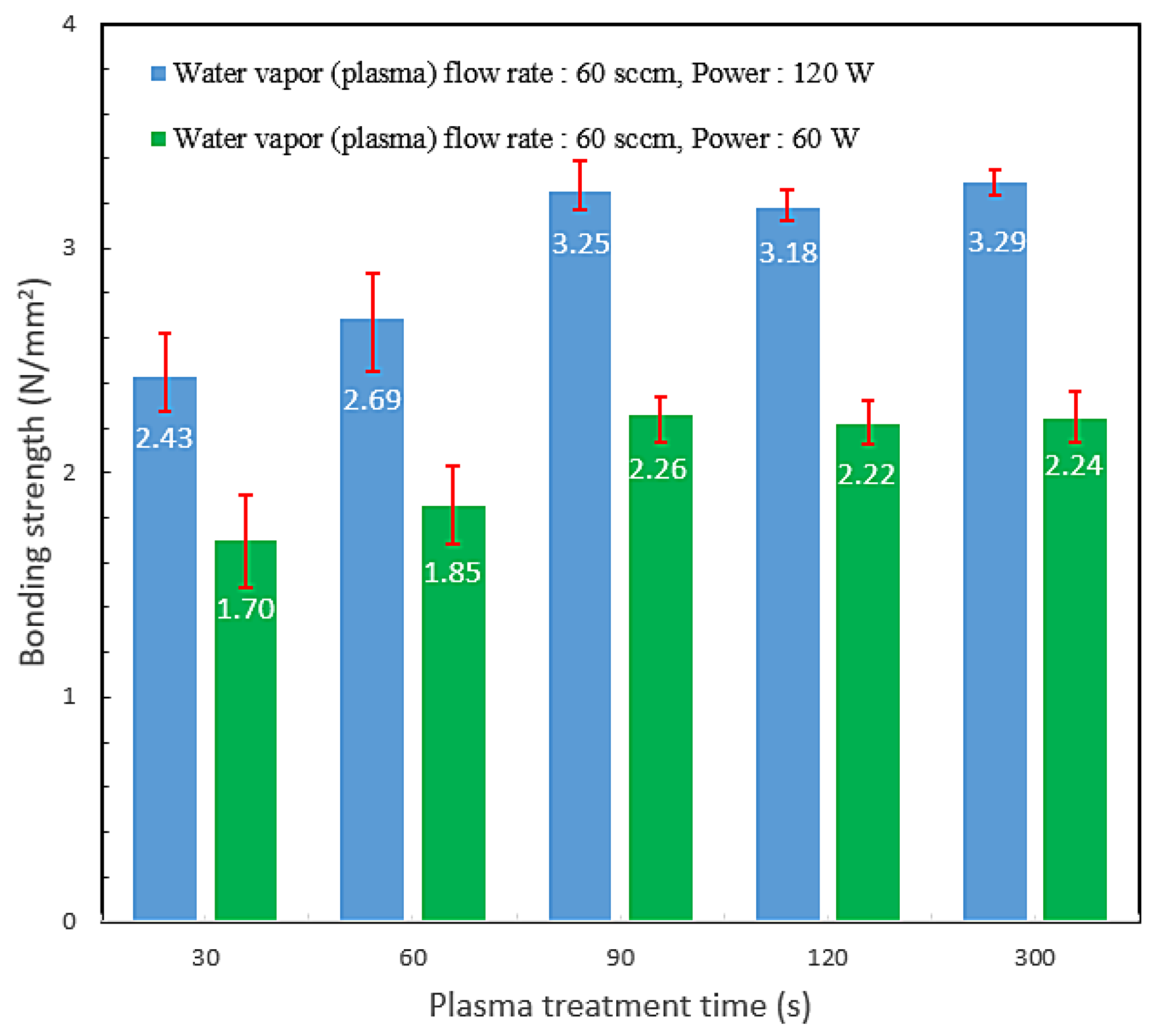
At a fixed gas flow rate of 60 sccm, the plasma treatment time was increased to 300 s. The time increased from 30 s to 60, 90, 120, and 300 s, as shown in Figure 7. There was no big increase in the bond strength with an increase in the plasma processing time from 90 s to 300 s. Using the plasma treatment process for heterogeneous bonding, there was no big increase in the bond strength for an increase in time from 90 s to 300 s, compared with that for the overall plasma treatment times. There was a slight changes in bond strength. This value increased from 3.25 N/mm2 (time of 90 s) to 3.29 N/mm2 (time of 300 s). If a low number of radicals was generated, then the non-thermal reaction process at room temperature did not change the OH aggregation, so the difference between plasma treatment times was small, 2.43 N/mm2 at 30 s and for 2.69 N/mm2 at 60 s. The overall bond strength increased by approximately 3.5%. During the plasma treatment process, the aggregation did not increase even with an increase in time. Thus, there was no effective increase in the bond strength. This occurred because the gas concentration had reached saturation in the chamber. After plasma treatment, the total surface energy of the sample surface increased. The polar groups included OH and C=O.
These functional groups generate free radicals. This phenomenon can be attributed to the gas flow rate and plasma power, where the higher the activation of the OH bonds, the higher the bond strength of the generated radicals. Occurrence of strong links and aggregation bonding reactions happens after plasma treatment at 120 W and 60 W. The bond strength increased from 1.70 N/mm2 to 2.24 N/mm2 at 30–300 s. Above 60 s, the bond strength increased gradually until reaching equilibrium ofter 90 s. Polymer chain entanglements effects and the amount generated diffuse radicals influence the bond strength. Prolonged holding time increases the generation of free radicals for the OH–OH bonds. The maximum bond strength achieved after 90 s of plasma processing time, i.e., 2.26 N/mm2. This upward trend is the same as for plasma treatment at 120 W. After plasma treatment at 120 W, there was an approximately 1.45 time increase in the bond strength over that produced at 60 W. The increase in bonding reactions on the sample surface leading to HO−OH aggregation of functional groups at the interface at stronger plasma powers and longer treatment times, which improves the bond strength.

3.3. Surface Morphology and Characteristics

The surface morphology of the PMMA and silicon samples after H2O plasma processing (plasma power: 120 W, gas flow rate: 60 sccm) was investigated. AFM images taken of the PMMA and silicon surfaces of the samples (without the plasma treatment) showed fine and smooth features. The surface roughness (Rmax) of the virgin PMMA and silicon was around 1.68 nm and 2.23 nm, respectively, as shown in Figure 8a,b. After being treated with the H2O plasma, the sample surface clearly revealed a fine node-dot structure. Formation of new functional groups increased the surface roughness, which was caused by enhanced surface energy through plasma [59]. Figure 8c,d shows the AFM images of the PMMA surfaces. The dimensions of the scanning surface of the samples was 3.0 × 3.0 μm2. Functional groups are comprised of groups of one or more atoms with distinctive chemical properties. OH bonds PMMA and silicon surfaces by functional groups, and other molecules bonded by covalent bonds, which cause the increase in roughness values. The simultaneous increase in the silanol density (Si−OH) on the silicon surfaces also creates better bonding strength and increases the roughness values. The 3D morphology observations of the surface roughness values of the samples produced by 90 s plasma treatment time are presented in Figure 8c,d. The surface roughness (Rmax) of the PMMA increases to 14.9 nm after a 30 s plasma treatment time, and the surface roughness (Rmax) of silicon increases to 30.2 nm after a 90 s plasma treatment time. The results show that there is a significant increment in the roughness of the PMMA and silicon surfaces after the H2O plasma treatment depending upon to treatment time. It is clear that the OH bonds in the plasma hit the surface more strongly than the H bonds, leading to a more effective surface morphology and that the O bonds for this range of gas flow rates do not influence the surface topography. This process was probably due to the oxidative cross-linking that typically occurs in many polymers upon exposure to atmospheric oxygen. Mutual bonding forces between covalent bonds change the roughness, which has a direct impact on the surface properties, especially in a room temperature bonding environment.

3.4. Optical Properties of the PMMA Layer

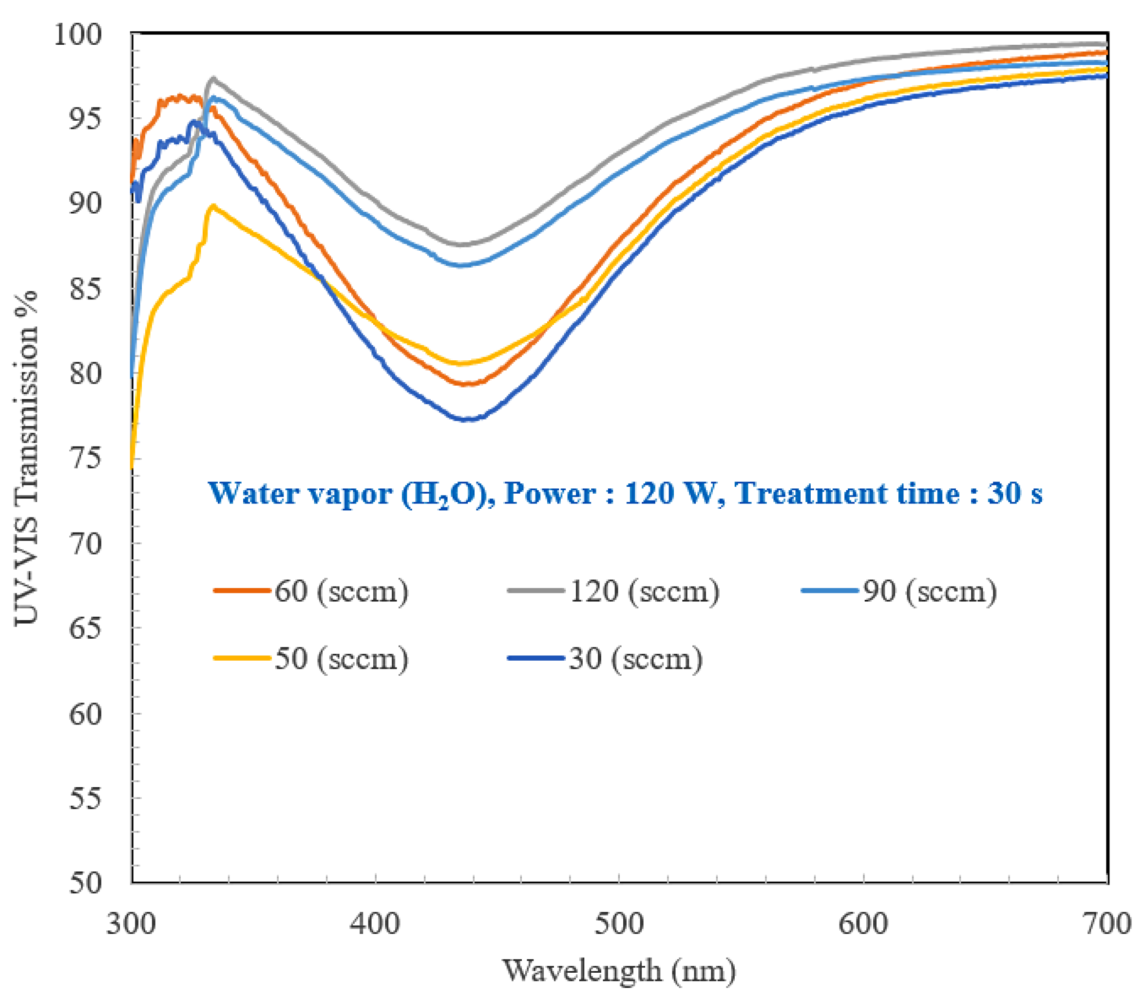
Above studies have shown the advantages of polymeric materials like PMMA because of their ease of fabrication, hemocompatibility and antibacterial properties [60]. Polymer substrates adapted for biometric screening applications, such as blood tests, must have good light permeability, biocompatibility and biostability. Such polymers have been extensively used in microfluidic devices. The main criteria for suitability include light transmittance and airtightness of the isolated polymer to protect the structure of enclosed layers from contamination through runners or holes in the interface. The microchannels have to retain good optical transmittance properties in the visible light region. (The UV–visible transmission spectra for our samples are shown in Figure 9). The measurement results show a large enhancement in the spectral intensity for the plasma treated samples produced with gas flow rates of 30, 50, 60, 90, and 120 sccm, from 89.5% (30 sccm) to 94.58% (120 sccm). The UV–visible transmission spectra show average spectral intensity of 90% to 94% light permeability in the visible region (400 nm to 700 nm). This result reveals that the samples have acceptable UV absorption up to 380 nm. As an example, the transmittance values at 380 nm (UV range) in the 400 to 700 nm (visible range) are illustrated in Figure 9.
In short, the PMMA samples are transparent in the visible region even after high gas flow rate processing. Comparing with the modified and virgin samples, there is no big difference in the spectra. All samples exhibit high transmission throughout the visible wavelength range, with an average transmittance of greater than 90%. Formation of H and OH bonds by plasma ionization and dissociation of water vapor by hydrogen bonding cause the excellent optical transparency in the visible region. The H2O plasma treatment lead to very strong transmittance for H3O+ bonds [61,62]. The light transmittance was considerably enhanced, to approximately 95% at 650 nm for a gas flow rate of 120 sccm. In the near-infrared region, H and OH bonds caused aggregations and O=C to form chains, creating numerous polymer groups leading to an average light transmittance of 96.45% from 600 nm to 700 nm. As discussed above and confirmed by the AFM images, the plasma treated specimens exhibited uniform surface roughness. Thus, high power and high gas flow rate plasma treatment can produce excellent interfacial adhesion and good light transmittance efficiency.

3.5. UV Fluorescence Inspection after Heterogeneous Bonding to Determine the Integrity, Morphology and Leakage of the Microchannels

The morphology of the bonding surfaces and interface was analyzed using AOI, FE-SEM and HR-TEM. AOI can also be used to detect defect areas and the flatness of the bonding interface in a microfluidic device. This system can link to the UV fluorescence mode, which are capable of accurately and quickly detecting the complete bonding interfaces of microfluidic devices and the micro channel morphology. At the same time, the observations are extremely useful to find if there is any leakage in the microchannels or at the bonding interface. After heterogeneous bonding, it is found that the walls of the microchannel are straight, without damage to their surface. Figure 10a shows the overall AOI shape and magnified views of the microchannel and the finished microchannel device after heterogeneous bonding (inset image). The observation areas after bonding are outlined in white. The observation shows the smooth microchannel without deformation in the connection are between the circular hole, as presented in Figure 10b. This result shows the PMMA substract with microchannel was successfully fabricated, with a width of 1000 μm, and very straight, as shown in Figure 10c. The connection between the upper hole and the side holes in the middle layer is very smooth and not deformed. Smooth surface wall of the microchannel in the through-hole area, as shown in Figure 10d. The AOI system can link the UV fluorescence mode (Green excitation fluorescence filter sets for an excitation wavelength range between 530–550 nm, G-2A, Nikon, Japan), making it capable of detecting the completeness of microfluidic devices. The observations are extremely useful for the detection of leakage in the microchannel morphology and at the bonded interface. Figure 10e shows an image of the area where the liquid passes through the heterogeneously bonded interface. The fluorescence response in cross-section at the bonded interface of the microchannel indicates whether there is leakage as the liquid passes through the upper layer through-hole into the lower microchannel; see the interface area in Figure 10e interface area. The bonding interface is flat and straight without any cracks; no leakage is observed. Combined with the above results, we can say that the PMMA and silicon substrates exhibited no evidence of defects in any areas in the microchannel after heterogeneous bonding. In other words, the test results show that the bonding process was lossless and perfect. The topography of the bonded interface of the microchannels is discussed below.
The final product with the highest bonded strength was selected for observation, and the plasma power and flow rate were 120 W and 60 sccm, respectively. Heterogeneous bonding of the microchannel device was carried out using plasma treatment at room temperature (25 °C) with a plasma treatment time of 90 s. The microchannels in the sample substrates with dimensions of 750 and 1000 μm in diameter and through-hole diameters between the upper and lower channels of 0.68 and 0.35 mm. The overall completeness of the microchannel device was studied, especially the interface where the DSP silicon sample was bonded to the upper and lower PMMA layers. The bonding interface was very flat. The effects of H2O plasma treatment can be explained in terms of the reactions of the Si−O−Si with incoming O bonds, with possible diffusion associated with the presence of water molecules at the interface. The reactions create Si−OH and OH−Si bonds across the interface resulting in covalent bonding. The FE-SEM image in Figure 11 a shows the interface of the sandwich after heterogeneous bonding; the thickness of the DSP silicon layer is 540 μm.
After being held for several seconds at the holding flow rate at room temperature, numerous OH radicals are generated on the surface producing a strong bonding force. Since this process is carried out at room temperature, there is no internal stress. Therefore, there will be no cracking due to stress of silicon in the heterojunction. The interface remains smooth and straight without damage, and finally, a lossless bonded interface is achieved. The samples of the microfluidic device produced after heterogeneous bonding were studied with HR-TEM. Figure 11b shows a cross-sectional HR-TEM image of the heterogeneous bonded interface with diffraction patterns. TEM diffraction confirms that this is single crystal silicon. There is no oxide layer on the bonding interface. The plasma treatment process, which was carried out at room temperature, does not easily produce an oxide layer on the surface of silicon. On the other hand, after a short period of time, the sample surface becomes hydrophilic and covered by a larger number of OH radicals. The bonding process results in a very clean sample surface after surface plasma activation. Past research has confirmed that the PMMA network prepared by radical polymerization is amorphous [63,64]. The amorphous halo visible in the HR-TEM diffraction pattern indicates that the sample is defect-free and very tightly bonded with the silicon, without gaps.

4. Conclusions

In this study, a convenient, lossless, and easy-to-operate method for plasma treatment at room temperature is demonstrated. PMMA was bonded promptly with a DPS wafer. We successfully demonstrate a simplified heterogeneous bonding process for a modular microfluidic device capable of on-site cell-based scheme detection of coagulation from the blood. The heterogeneous bonded substrate designed to be used in microfluidic devices was achieved through free radical polymerization and the interaction of molecular OH bonds produced during a plasma bonding process carried out at close to room temperature. After H2O plasma processing is completed, the morphology of the PMMA substrate was characterized. It was found to be flat with high transmittance and perfect bonding quality. No leakage or crack high stability of the microchannels was observed in the cross-sectional AOI system images of the heterogeneous bonding interface. This treatment process was combined with a controlled H2O gas flow rate to produce sandwich substrates. The results show perfect lossless interface bonding quality. The gas flow rate of the plasma is extremely important for the process of activation in the heterogeneous bonding process at room temperature. A sandwich substrate was successfully bonded at room temperature by plasma bonding method without any deformation, and it was confirmed by FE-SEM and HR-TEM observations. The bond strength obtained using the H2O plasma treatment was examined for different gas flow rates and power. The bond strength increased even at room temperature when the plasma treatment method was used. This method is suitable for the fabrication of high-quality, rapid-acting and low cost microfluidic devices to be used for quick checks of biological compounds and for the analysis of blood samples. Such technology can be applied for the production of rapid single-time measurement devices requiring small amounts of reagent. The analysis of whole blood and single cell capture. In coagulation research, micro-channels have the same characteristic size as blood composition. So, microfluidic devices allow exact manipulations of the process by which blood changes from a liquid to a gel drug.

Author Contributions

C.-C.C. contributed to the design, experimental work and data collection for this article; P.N.I. contributed to writing the original draft, preparation for this article and validation; Y.-H.C. contributed the software; S.-J.H. offered supervision and funding acquisition. All authors have read and agreed to the published version of the manuscript.

Funding

The authors would like to thank the Ministry of Science and Technology, Republic of China (Taiwan), for their support of this research under contract number: MOST 109-2224-E-011-002.

Data Availability Statement

Not applicable.

Conflicts of Interest

The authors declare no conflict of interest.

References

  1. Song, I.-H.; Park, T. PMMA solution assisted room temperature bonding for PMMA–PC hybrid devices. Micromachines 2017, 8, 284. [Google Scholar] [CrossRef] [Green Version]
  2. Tran, H.H.; Wu, W.; Lee, N.Y. Ethanol and UV-assisted instantaneous bonding of PMMA assemblies and tuning in bonding reversibility. Sens. Actuators B Chem. 2013, 181, 955–962. [Google Scholar] [CrossRef]
  3. Chen, Z.; Gao, Y.; Lin, J.; Su, R.; Xie, Y. Vacuum-assisted thermal bonding of plastic capillary electrophoresis microchip imprinted with stainless steel template. J. Chromatogr. A 2004, 1038, 239–245. [Google Scholar] [CrossRef]
  4. Koval, Y. Mechanism of etching and surface relief development of PMMA under low-energy ion bombardment. J. Vac. Science Technol. B Microelectron. Nanometer Struct. Process. Meas. Phenom. 2004, 22, 843–851. [Google Scholar] [CrossRef]
  5. Funano, S.-I.; Ota, N.; Sato, A.; Tanaka, Y. A method of packaging molecule/cell-patterns in an open space into a glass microfluidic channel by combining pressure-based low/room temperature bonding and fluorosilane patterning. Chem. Commun. 2017, 53, 11193–11196. [Google Scholar] [CrossRef] [PubMed]
  6. Amirfeiz, P.; Bengtsson, S.; Bergh, M.; Zanghellini, E.; Börjesson, L. Formation of silicon structures by plasma-activated wafer bonding. J. Electrochem. Soc. 2000, 147, 2693. [Google Scholar] [CrossRef]
  7. Dong, P.; Chen, Y.-K.; Duan, G.-H.; Neilson, D.T. Silicon photonic devices and integrated circuits. Nanophotonics 2014, 3, 215–228. [Google Scholar] [CrossRef]
  8. Yang, H.; Huang, M.; Wu, J.; Lan, Z.; Hao, S.; Lin, J. The polymer gel electrolyte based on poly (methyl methacrylate) and its application in quasi-solid-state dye-sensitized solar cells. Mater. Chem. Phys. 2008, 110, 38–42. [Google Scholar] [CrossRef]
  9. Chen, Y.; Duan, H.; Zhang, L.; Chen, G. Fabrication of PMMA CE microchips by infrared-assisted polymerization. Electrophoresis 2008, 29, 4922–4927. [Google Scholar] [CrossRef]
  10. Fung, C.K.; Zhang, M.Q.; Chan, R.H.; Li, W.J. In A PMMA-based micro pressure sensor chip using carbon nanotubes as sensing elements. In Proceedings of the 18th IEEE International Conference on Micro Electro Mechanical Systems, Miami Beach, FL, USA, 30 January–3 February 2005; pp. 251–254. [Google Scholar]
  11. Hong, J.; Lee, S.; Seo, J.; Pyo, S.; Kim, J.; Lee, T. A highly sensitive hydrogen sensor with gas selectivity using a PMMA membrane-coated Pd nanoparticle/single-layer graphene hybrid. ACS Appl. Mater. Interfaces 2015, 7, 3554–3561. [Google Scholar] [CrossRef]
  12. Mathur, A.; Roy, S.; Tweedie, M.; Mukhopadhyay, S.; Mitra, S.; McLaughlin, J. Characterisation of PMMA microfluidic channels and devices fabricated by hot embossing and sealed by direct bonding. Curr. Appl. Phys. 2009, 9, 1199–1202. [Google Scholar] [CrossRef]
  13. Romoli, L.; Tantussi, G.; Dini, G. Experimental approach to the laser machining of PMMA substrates for the fabrication of microfluidic devices. Opt. Lasers Eng. 2011, 49, 419–427. [Google Scholar] [CrossRef]
  14. Xu, J.; Locascio, L.; Gaitan, M.; Lee, C.S. Room-temperature imprinting method for plastic microchannel fabrication. Anal. Chem. 2000, 72, 1930–1933. [Google Scholar] [CrossRef] [PubMed]
  15. Mair, D.A.; Rolandi, M.; Snauko, M.; Noroski, R.; Svec, F.; Fréchet, J.M. Room-temperature bonding for plastic high-pressure microfluidic chips. Anal. Chem. 2007, 79, 5097–5102. [Google Scholar] [CrossRef]
  16. Takagi, H.; Kikuchi, K.; Maeda, R.; Chung, T.; Suga, T. Surface activated bonding of silicon wafers at room temperature. Appl. Phys. Lett. 1996, 68, 2222–2224. [Google Scholar] [CrossRef]
  17. Howlader, M.; Zhang, F.; Kibria, M. Void nucleation at a sequentially plasma-activated silicon/silicon bonded interface. J. Micromechanics Microeng. 2010, 20, 065012. [Google Scholar] [CrossRef]
  18. Matsumae, T.; Fengwen, M.; Fukumoto, S.; Hayase, M.; Kurashima, Y.; Higurashi, E.; Takagi, H.; Suga, T. Heterogeneous GaN-Si integration via plasma activation direct bonding. J. Alloys Compd. 2021, 852, 156933. [Google Scholar] [CrossRef]
  19. Howlader, M.; Suehara, S.; Takagi, H.; Kim, T.; Maeda, R.; Suga, T. Room-temperature microfluidics packaging using sequential plasma activation process. IEEE Trans. Adv. Packag. 2006, 29, 448–456. [Google Scholar] [CrossRef]
  20. Budraa, N.K.; Jackson, H.; Barmatz, M.; Pike, W.T.; Mai, J.D. In Low pressure and low temperature hermetic wafer bonding using microwave heating, Technical Digest. In Proceedings of the IEEE International MEMS 99 Conference. Twelfth IEEE International Conference on Micro Electro Mechanical Systems (Cat. No. 99CH36291), Orlando, FL, USA, 21 January 1999; pp. 490–492. [Google Scholar]
  21. Ashraf, M.W.; Tayyaba, S.; Afzulpurkar, N. Micro electromechanical systems (MEMS) based microfluidic devices for biomedical applications. Int. J. Mol. Sci. 2011, 12, 3648–3704. [Google Scholar] [CrossRef]
  22. Tsao, C.; Hromada, L.; Liu, J.; Kumar, P.; DeVoe, D. Low temperature bonding of PMMA and COC microfluidic substrates using UV/ozone surface treatment. Lab Chip 2007, 7, 499–505. [Google Scholar] [CrossRef]
  23. Frazer, R.Q.; Byron, R.T.; Osborne, P.B.; West, K.P. PMMA: An essential material in medicine and dentistry. J. Long-Term Eff. Med Implant. 2005, 15, 629–639. [Google Scholar] [CrossRef] [PubMed] [Green Version]
  24. Ma, X.; Li, R.; Jin, Z.; Fan, Y.; Zhou, X.; Zhang, Y. Injection molding and characterization of PMMA-based microfluidic devices. Microsyst. Technol. 2020, 26, 1317–1324. [Google Scholar] [CrossRef]
  25. Roman, G.T.; Hlaus, T.; Bass, K.J.; Seelhammer, T.G.; Culbertson, C.T. Sol−gel modified poly (dimethylsiloxane) microfluidic devices with high electroosmotic mobilities and hydrophilic channel wall characteristics. Anal. Chem. 2005, 77, 1414–1422. [Google Scholar] [CrossRef] [PubMed]
  26. Lin, R.; Burns, M.A. Surface-modified polyolefin microfluidic devices for liquid handling. J. Micromech. Microeng. 2005, 15, 2156. [Google Scholar] [CrossRef] [Green Version]
  27. Chen, C.-S.; Breslauer, D.N.; Luna, J.I.; Grimes, A.; Chin, W.-c.; Lee, L.P.; Khine, M. Shrinky-Dink microfluidics: 3D polystyrene chips. Lab A Chip 2008, 8, 622–624. [Google Scholar] [CrossRef]
  28. Fan, Y.; Li, H.; Yi, Y.; Foulds, I.G. PMMA to Polystyrene bonding for polymer based microfluidic systems. Microsyst. Technol. 2014, 20, 59–64. [Google Scholar] [CrossRef]
  29. Yu, H.; Chong, Z.; Tor, S.; Liu, E.; Loh, N. Low temperature and deformation-free bonding of PMMA microfluidic devices with stable hydrophilicity via oxygen plasma treatment and PVA coating. RSC Adv. 2015, 5, 8377–8388. [Google Scholar] [CrossRef]
  30. Ashok, P.C.; Dholakia, K. Microfluidic Raman spectroscopy for bio-chemical sensing and analysis. In Optical Nano-and Microsystems for Bioanalytics; Springer: Berlin/Heidelberg, Germany, 2012; pp. 247–268. [Google Scholar]
  31. Vollrath, A.; Pretzel, D.; Pietsch, C.; Perevyazko, I.; Schubert, S.; Pavlov, G.M.; Schubert, U.S. Preparation, cellular internalization, and biocompatibility of highly fluorescent PMMA nanoparticles. Macromol. Rapid Commun. 2012, 33, 1791–1797. [Google Scholar] [CrossRef]
  32. Roy, S.; Yue, C.; Wang, Z.; Anand, L. Thermal bonding of microfluidic devices: Factors that affect interfacial strength of similar and dissimilar cyclic olefin copolymers. Sens. Actuators B Chem. 2012, 161, 1067–1073. [Google Scholar] [CrossRef]
  33. Brown, L.; Koerner, T.; Horton, J.H.; Oleschuk, R.D. Fabrication and characterization of poly (methylmethacrylate) microfluidic devices bonded using surface modifications and solvents. Lab Chip 2006, 6, 66–73. [Google Scholar] [CrossRef]
  34. Bagiatis, V.; Critchlow, G.; Price, D.; Wang, S. The effect of atmospheric pressure plasma treatment (APPT) on the adhesive bonding of poly (methyl methacrylate)(PMMA)-to-glass using a polydimethylsiloxane (PDMS)-based adhesive. Int. J. Adhes. Adhes. 2019, 95, 102405. [Google Scholar] [CrossRef]
  35. Pfleging, W.; Baldus, O. Laser Patterning and Welding of Transparent Polymers for Microfluidic Device Fabrication, Laser-Based Micropackaging; International Society for Optics and Photonics: Bellingham, WA, USA, 2006; p. 610705. [Google Scholar]
  36. Chen, X.; Shen, J.; Zhou, M. Rapid fabrication of a four-layer PMMA-based microfluidic chip using CO2-laser micromachining and thermal bonding. J. Micromech. Microeng. 2016, 26, 107001. [Google Scholar] [CrossRef]
  37. Ali, U.; Karim, K.J.B.A.; Buang, N.A. A review of the properties and applications of poly (methyl methacrylate) (PMMA). Polym. Rev. 2015, 55, 678–705. [Google Scholar] [CrossRef]
  38. Lynh, H.D.; Pin-Chuan, C. Novel solvent bonding method for creation of a three-dimensional, non-planar, hybrid PLA/PMMA microfluidic chip. Sens. Actuators A Phys. 2018, 280, 350–358. [Google Scholar] [CrossRef]
  39. Terai, H.; Funahashi, R.; Hashimoto, T.; Kakuta, M. Heterogeneous bonding between cyclo-olefin polymer (COP) and glass-like substrate by newly developed water vapor-assisted plasma, Aqua Plasma Cleaner. Electr. Eng. Jpn. 2018, 205, 48–56. [Google Scholar] [CrossRef]
  40. Immanuel, P.N.; Chao-Ching, C.; Yang, C.-R.; Subramani, M.; Lee, T.-H.; Huang, S.-J. Surface activation of poly (methyl methacrylate) for microfluidic device bonding through a H2O plasma treatment linked with a low-temperature annealing. J. Micromech. Microeng. 2021, 31, 055004. [Google Scholar]
  41. Tang, L.; Lee, N.Y. A facile route for irreversible bonding of plastic-PDMS hybrid microdevices at room temperature. Lab Chip 2010, 10, 1274–1280. [Google Scholar] [CrossRef]
  42. Aran, K.; Sasso, L.A.; Kamdar, N.; Zahn, J.D. Irreversible, direct bonding of nanoporous polymer membranes to PDMS or glass microdevices. Lab Chip 2010, 10, 548–552. [Google Scholar] [CrossRef] [Green Version]
  43. Liston, E.; Martinu, L.; Wertheimer, M. Plasma surface modification of polymers for improved adhesion: A critical review. J. Adhes. Sci. Technol. 1993, 7, 1091–1127. [Google Scholar] [CrossRef]
  44. Zeng, W.; Li, S.; Chow, W.K. Review on chemical reactions of burning poly (methyl methacrylate) PMMA. J. Fire Sci. 2002, 20, 401–433. [Google Scholar] [CrossRef]
  45. Matsutani, A.; Ohtsuki, H.; Koyama, F. Characterization of H2O-inductively coupled plasma for dry etching. J. Phys. Conf. Ser. 2008, 100, 062022. [Google Scholar] [CrossRef]
  46. Annušová, A.; Krištof, J.; Veis, P.; Foissac, C.; Supiot, P. Spectroscopic study of an Ar-H2O discharge excited by a RF helical cavity. WDS’12 Proc. Contrib. Pap. 2012, 2, 99–104. [Google Scholar]
  47. Tennico, Y.H.; Koesdjojo, M.T.; Kondo, S.; Mandrell, D.T.; Remcho, V.T. Surface modification-assisted bonding of polymer-based microfluidic devices. Sens. Actuators B Chem. 2010, 143, 799–804. [Google Scholar] [CrossRef]
  48. Wang, R.; Shen, Y.; Zhang, C.; Yan, P.; Shao, T. Comparison between helium and argon plasma jets on improving the hydrophilic property of PMMA surface. Appl. Surf. Sci. 2016, 367, 401–406. [Google Scholar] [CrossRef]
  49. Lee, W.-J.; Chang, J.-G.; Ju, S.-P. Hydrogen-bond structure at the interfaces between water/poly (methyl methacrylate), water/poly (methacrylic acid), and water/poly (2-aminoethylmethacrylamide). Langmuir 2010, 26, 12640–12647. [Google Scholar] [CrossRef]
  50. ASTM D638-14:2014. Standard Test Method for Tensile Properties of Plastics; ASTM International: West Conshohocken, PA, USA, 2014. [Google Scholar]
  51. Ravarian, R.; Wei, H.; Rawal, A.; Hook, J.; Chrzanowski, W.; Dehghani, F. Molecular interactions in coupled PMMA–bioglass hybrid networks. J. Mater. Chem. B 2013, 1, 1835–1845. [Google Scholar] [CrossRef]
  52. Joonlapak, K.; Wiwattanakul, P.; Jirathampradhab, T.; Akhadejdamrong, T.; Wongariyakawee, A.; Srikhirin, T. The Preparation of Highly Transparent Layered Double Hydroxides (LDHs)-Poly (Methyl Methacrylate) (PMMA) Nanocomposites Sheets by Batch Cell Polymerization Method. In IOP Conference Series: Materials Science and Engineering; IOP Publishing: Bristol, UK, 2019; p. 012009. [Google Scholar]
  53. Abdel–Fattah, E. Surface activation of poly (methyl methacrylate) with atmospheric pressure ar+ h2o plasma. Coatings 2019, 9, 228. [Google Scholar] [CrossRef] [Green Version]
  54. Pan, Y.V.; Denton, D.D. Plasma dissociation reaction kinetics. I. Methyl Methacrylate J. Appl. Polym. Sci. 1999, 73, 1–16. [Google Scholar]
  55. Bamshad, A.; Nikfarjam, A.; Khaleghi, H. A new simple and fast thermally-solvent assisted method to bond PMMA–PMMA in micro-fluidics devices. J. Micromech. Microeng. 2016, 26, 065017. [Google Scholar] [CrossRef]
  56. Gilliam, M.; Farhat, S.; Zand, A.; Stubbs, B.; Magyar, M.; Garner, G. Atmospheric plasma surface modification of PMMA and PP micro-particles. Plasma Process. Polym. 2014, 11, 1037–1043. [Google Scholar] [CrossRef]
  57. Shimizu, M. Ion chemistry in the cometary atmosphere. Astrophys. Space Sci. 1975, 36, 353–361. [Google Scholar] [CrossRef]
  58. Wang, C.; Wang, Y.; Tian, Y.; Wang, C.; Suga, T. Room-temperature direct bonding of silicon and quartz glass wafers. Appl. Phys. Lett. 2017, 110, 221602. [Google Scholar] [CrossRef]
  59. Shobhana, E. X-Ray diffraction and UV-visible studies of PMMA thin films. Int. J. Mod. Eng. Res. 2012, 2, 1092–1095. [Google Scholar]
  60. Saggiomo, V.; Velders, A.H. Simple 3D printed scaffold-removal method for the fabrication of intricate microfluidic devices. Adv. Sci. 2015, 2, 1500125. [Google Scholar] [CrossRef]
  61. Shah, J.J.; Geist, J.; Locascio, L.E.; Gaitan, M.; Rao, M.V.; Vreeland, W.N. Capillarity induced solvent-actuated bonding of polymeric microfluidic devices. Anal. Chem. 2006, 78, 3348–3353. [Google Scholar] [CrossRef]
  62. Kotz, F.; Mader, M.; Dellen, N.; Risch, P.; Kick, A.; Helmer, D.; Rapp, B.E. Fused deposition modeling of microfluidic chips in polymethylmethacrylate. Micromachines 2020, 11, 873. [Google Scholar] [CrossRef]
  63. Dorranian, D.; Abedini, Z.; Hojabri, A.; Ghoranneviss, M. Structural and optical characterization of PMMA surface treated in low power nitrogen and oxygen RF plasmas. J. Non-Oxide Glasses 2009, 1, 217–229. [Google Scholar]
  64. Jafari, M.; Dorranian, D. Surface modification of PMMA polymer in the interaction with oxygen-argon RF plasma. J. Theor. Appl. Phys. 2011, 5, 59–66. [Google Scholar]
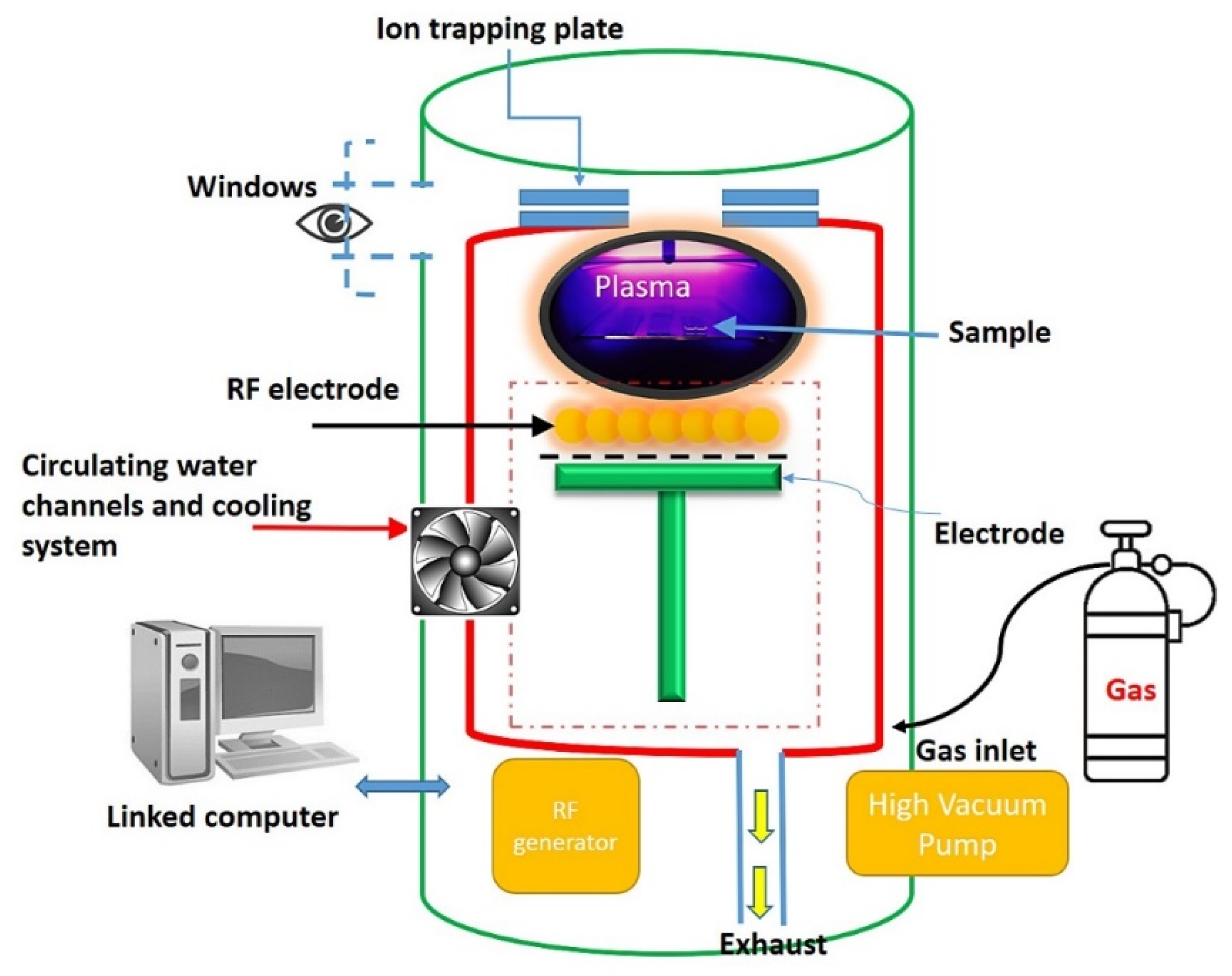
Figure 1. The schematic diagram of the H2O plasma treatment for PMMA and silicon bonding activation.
Coatings 11 00580 g001
Figure 2. (a,b) Schematic illustration of the bonded sample for tensile testing. (c) 3D model of the tensile test (ASTM D638, type V); dimensions of the tensile test sample: width (9.53 mm) and length (63.5 mm). (d) MTS criterion test system. (e) Complete tensile test sample for microfluidic device H2O plasma bonding.
Coatings 11 00580 g002
Figure 3. Process flow diagram for bonding between PMMA/silicon substrates. (a) Chemical structures of the PMMA substrates. (b) Schematic illustration of the chemical reaction caused by the incorporation of H2O plasma in the bonding process on the surface of the substrates. (c) Chemical reaction anticipated to occur on the surfaces of the PMMA and silicon substrates after H2O plasma treatment, resulting in bonded H2O–OH+ radicals.
Coatings 11 00580 g003
Figure 4. OES after applying of pressurized H2O plasma for sample treatment at a fixed (2.8 kVpp) discharge voltage. At this condition, the OH radical spectrum has a very high intensity at plasma powers of 30, 60, 90 and 120 W.
Coatings 11 00580 g004
Figure 5. Emission intensities of the OH (307 nm) and H bonds (486 nm) as a function of the application of pressurized H2O plasma.
Coatings 11 00580 g005
Figure 6. (a) Intensity of the O bonds (844 nm and 926 nm) emission lines as a function of gas flow rate. (b) Bonding strength with standard deviation of the heterogeneous bond strengths of PMMA/silicon substrates after H2O plasma treatment at gas flow rates of 30, 50, 60, 90 and 120 sccm, with plasma powers of 60 and 120 W.
Coatings 11 00580 g006
Figure 7. Bond strength of sample substrates with the standard deviation after H2O plasma treatment showing dependence of the bond strength on plasma treatment time: 30 s to 300 s (gas flow rate: 60 sccm; maximum bond strength: 3.29 N/mm2). The order is as follows: 2.43, 2.69, 3.25, 3.18 N/mm2 for a 60 W plasma treatment for 1.70, 1.85, 2.26, 2.22, and 2.24 N/mm2.
Coatings 11 00580 g007
Figure 8. Surface roughness of the pristine (a) PMMA and (b) silicon. (c) 3D AFM images of the PMMA sample after a 90 s plasma treatment time and (d) of the silicon sample after a 90 s H2O plasma treatment time.
Coatings 11 00580 g008
Figure 9. UV–visible transmission spectrum for our samples after a plasma treatment time of 30 s, for flow rates of: 30, 50, 60, 90, to 120 sccm; power: 120 W.
Coatings 11 00580 g009
Figure 10. Morphology of the microchannels after heterogeneous bonding was observed by AOI. (a) Complete microchannel device fabricated by heterogeneous bonding. (b) The morphology of the microchannels and through-holes is smooth and flat, without deformation or leakage in the linking area between the channels and the circular holes. (c) The width of the microchannel is 1000 μm. (d) The diameter of the through-hole is 750 μm, which results in no damage and smooth surface wall. (e) Photograph of the interface microchannel in UV fluorescence mode.
Coatings 11 00580 g010
Figure 11. (a) Lossless bonded interface of the microfluidic device (PMMA/silicon/PMMA). (b) HR-TEM image of the bonded interface with diffraction patterns.
Coatings 11 00580 g011
Table 1. Heterogeneous bond strengths after plasma treatment.
H2O Flow Rate (sccm)30506090120
Power 120 W, Bond strength (N/mm2)1.562.182.431.681.32
Power 60 W, Bond strength (N/mm2)1.081.521.71.10.94
Publisher’s Note: MDPI stays neutral with regard to jurisdictional claims in published maps and institutional affiliations.