Abstract
This study proposes a method for measuring curved-mechanical characteristics based on a whole-folding test for transparent conductive film-coated polymer substrates using common-path optical interferometry. Accordingly, 80-, 160-, and 230-nm indium tin oxide films coated on 40 × 40 mm 125-μm-thick polyethylene terephthalate (PET) substrates, and monolayer graphene films coated on 40 × 40 mm 250-μm-thick PET substrates are inspected and analyzed under the curving conditions of 50-, 30-, 20-, and 10-mm radii before and after an 11,000 whole-folding cycle test based on a 10-mm folding radius. This study utilizes the changes in the phase retardations of transparent conductive film-coated polymer substrates under different curving conditions before and after 11,000 whole-folding cycles to analyze the substrates’ residual stress characteristics that were the direct result of manufacturing process parameters. The results from this study of curved-mechanical characteristic measurements of flexible transparent conductive substrates can provide designers with improved product development and can assist manufacturers in improving the manufacturing design of enhanced coating processes.
1. Introduction
Flexible substrates are critical components of flexible electronics. Because different flexible electronic product applications have different requirements for substrate materials, research on substrate materials determines the developmental direction of flexible electronics. For example, magnetic material films or nanoparticles are deposited on transparent flexible substrates (e.g., polyethylene terephthalate (PET), polyimide, polystyrene, polymethylmethacrylate, or cyclic olefin copolymer) for developments of magnetic sensors or absorbers [1,2,3,4,5]. Because the flexible transparent optical film itself is not conductive, depositing a transparent conductive film on it as a conductive electrode (e.g., indium tin oxide (ITO) or aluminum doped zinc oxide) is necessary. The current commonly-used transparent conductive material is an ITO film, which has the advantages of low resistivity (1–5 × 10⁻⁶ Ωm) and high light transmittance. In recent years, ITO conductive oxides have been deposited on PET plastic films. This represents one of the most popular research directions for flexible electronic materials [6,7,8,9]. However, after depositing the flexible transparent optical or conductive film on the polymer substrate, it still exhibits poor water and oxygen resistance, temperature, humidity, and mechanical properties of load conditions. Accordingly, major domestic and foreign manufacturers and research institutes are seeking alternatives. Therefore, in recent years, for the application of flexible substrates or sensors, graphene materials have been added to improve the conductivity, mechanical properties, electromagnetic effects, heat conduction effects, and optical transmittance of flexible transparent optical films [10,11,12,13,14]. For quality mechanical measurements of graphene film materials, most studies have used non-contact Raman spectroscopy [15,16,17,18,19]; others have used atomic force microscopy [20,21,22]. These mechanical characteristic measurements require precision and expensive equipment, such as Raman spectrometers and atomic force microscopes, and the measurement range can be as high as hundreds of microns. For large deformations of flexible electronics, the bending radius of curvature is approximately millimeters to centimeters. For large areas, fast confirmation and further analysis of the interface stress of flexible graphene substrates are difficult, and the cost of high detection equipment is considerable for general manufacturers. In addition, the major features of flexible electronics are the bending storage and operation of curving conditions, such as the display or transmission of electrical signals during curving [23,24,25]. Therefore, flexible electronic stress analysis under curving conditions enables researchers to obtain an improved design for enhanced coating processes. Some studies [26,27,28] have utilized optical phase retardation measurement technology to measure the stress states of transparent materials. Of these technologies, single-point [29,30,31], area-based [32,33,34,35], and area-based optical phase retardation measurement methods with scanning platforms [36,37,38] have been used. In addition, some literatures utilize an X-ray reflectometer to analyze the stresses of the films [39,40,41]. However, to measure and analyze stress states, measured states must be under the plane. Therefore, this study proposes a method for measuring the curved-mechanical characteristics of transparent conductive film-coated polymer substrates using common-path optical interferometry. To analyze the mechanical characteristics of transparent conductive film-coated PET substrates in curving, an automatic sliding-folding testing platform (ASTP) [42] is used to conduct a whole-folding test in this study. Accordingly, 80-, 160-, and 230-nm ITO films coated on 40 × 40 mm 125-μm-thick PET substrates and monolayer graphene films coated on 40 × 40 mm 250-μm-thick PET substrates were inspected and analyzed under the curving conditions of 50-, 30-, 20-, and 10-mm radii before and after an 11,000 whole-folding cycle test based on a 10-mm folding radius was conducted. The curved-mechanical characteristic measurement results of flexible transparent conductive substrates can provide designers with improved product development or assist manufacturers in improving the manufacturing design of enhanced coating processes.
2. Methods
To measure and analyze the curved-mechanical characteristics of transparent conductive film-coated polymer substrates, this study develops a common-path optical interferometric technique to measure the phase retardations of a sample on a curved clamper, as shown in Figure 1. The light from a flat white light source passes through a color filter and a PR polarizer and is thus transformed into a linearly polarized light at 45° to the y axis. The light next passes through a liquid crystal modulation and a tested sample on a curved clamper with an r radius of curvature. The light then passes through an AR analyzer with a transmission axis at −45° to the y axis, and finally through an imaging lens and camera to obtain the phase retardations of the sample during curving. Because the collimated light transmitted to the transparent curved test sample causes refraction and phase retardation, this study derives the phase retardation influence factor in curving. The phase retardation under the curving of the test sample is next measured using common-path optical interferometry. Finally, the phase retardation influence factor in curving is subtracted from it, and the phase retardation of the sample in curving is obtained.

Figure 1.
Schematic of phase retardation measurements under the curving of a test sample by common-path optical interferometry.
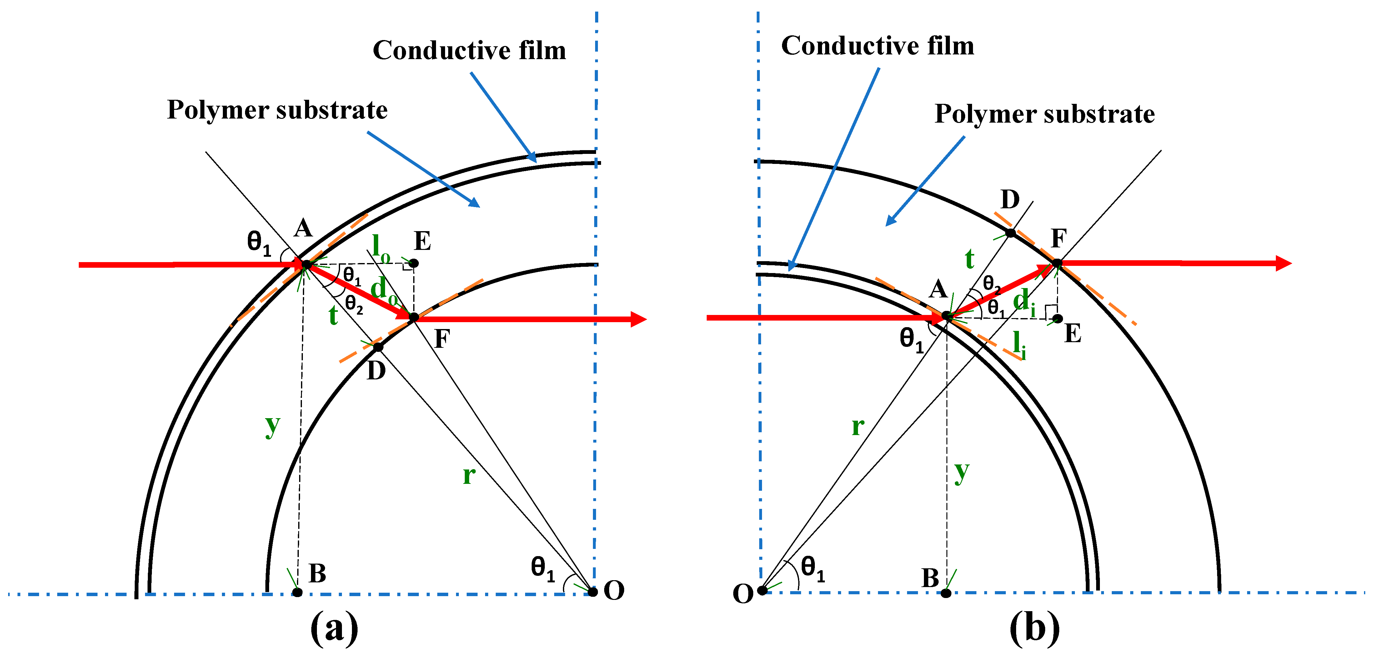
Because the thickness of the transparent conductive film of the test sample is much lower than that of the polymer substrate, this study considers only the refraction effect of the polymer substrate under curving, as shown in Figure 2. Figure 2a,b shows the optical paths of the test sample of the collimated light source transmission under outer and inner curves.
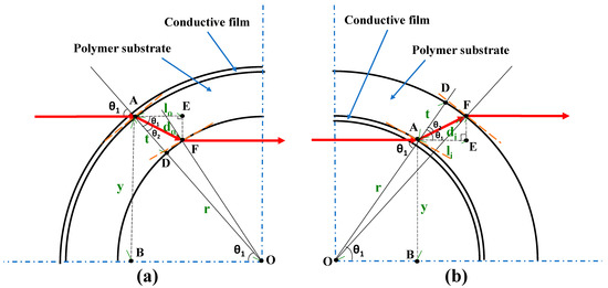
Figure 2.
Optical paths of the test sample of the collimated light source transmission under (a) outer and (b) inner curves, where the vertical, horizontal, and perpendicular directions are the y, z, and x axes, respectively.
In Figure 2, the curving radius r is based on the curving center O. According to Snell’s law [27], the following equation is obtained:
where and are the refractive indices of the air and polymer substrate, respectively, is the incident angle of point A, and is the refraction angle. According to the ABO, under the outer curve, the following equation is obtained:
and under the inner curve, the following equation is obtained:
where is the distance between point A and the incident light beam on the sample and the extension point B from the center of the curve, and is the thickness of the sample based on the extremely thin transparent conductive film. In the AFD under the outer and inner curves, the approximate relationship can be expressed as [43]
where is the path of the light passing through the sample. Through the trigonometric function relationship of , under the outer curve, can be rewritten as
and under the inner curve, can be rewritten as
From the geometric relationship of AFE and the angle formula of the trigonometric function, under the outer curving, is derived as
and under the inner curving, is derived as
Figure 2 shows only the upper half of the y axis, and because the lower half is symmetrical with the upper half, the phase retardation of the lower half is added to the upper half. Therefore, according to the definition of optical phase retardation [43], the phase retardation of the flexible transparent conductive film-coated polymer substrate with or without curving under outer curving is
and the phase retardation of the flexible transparent conductive film-coated polymer substrate with or without curving under inner curving is
Therefore, and are the phase-retardation influence factors in the outer and inner curving, respectively. According to the literature [27,44], the light amplitude in Figure 1 using common-path optical interferometry is derived as
where a polarizer and analyzer with 45° and 135° linearly polarized directions PR and AR to the y axis, respectively, are and , respectively. and are the Jones matrix of the tested sample and Jones vector of the light at the x axis [27], respectively, where is the total optical retardation of the multilayer-film substrate. In addition, is the Jones matrix of n-layer liquid crystal modulation based on a twisted nematic liquid crystal with a maximum twist angle of 90°, which is written as
According to [44], the 2D phase-retardation distribution by common-path optical interferometry is derived as
Because the collimated light transmitted to the transparent curved test sample causes refraction and phase retardation, this study utilizes the phase-retardation influence factors of (9) and (10) subtracted from (13) based on the method of 2D phase unwrapping [45] to obtain the correct phase retardation of the sample during curving. Finally, the correct phase retardation of the sample in the outer curving is derived as
and the correct phase retardation of the sample in inner curving is derived as
3. Experiment
Figure 3 depicts the instrument configuration of the phase retardation measurements of the test sample under a curving with a 30-mm radius by common-path optical interferometry. To avoid light interference, this study measured the phase retardation of the sample in a dark room. In this study, a flat white light source with a color filter, PR, and liquid crystal modulation was used as a linearly polarized white light with a 535.38-nm central wavelength; this was a liquid crystal flat panel display. This study also utilized a 1388 × 1038-pixel camera (Basler/A631fc) with an AR analyzer in front to capture phase retardation images. Finally, liquid crystal modulation was controlled to perform four-step phase shifting [46] for 0, 1/6, 1/3, and 1/2 maximum intensities, image processing, and correction calculations, which was necessary to measure the optical retardation images under the curving of the test sample using LabVIEW software. Each phase retardation measurement was the average value of 15 measurement images. In this study, four curved clampers with radii of 10, 20, 30, and 50 mm were used to provide four corresponding curving conditions of the test sample, as shown in Figure 4. In addition, each curved clamper had a measurement area of 10 × 10 mm or greater. Figure 5 depicts a 125-μm-thick PET substrate and 80-, 160-, and 230-nm ITO films coated on 40 × 40 mm 125-μm-thick PET substrates (VisionTek Systems Ltd., Chester, UK). Monolayer graphene films coated on 40 × 40 mm 250-μm-thick PET substrates (Graphenea Inc., Cambridge, MA, USA) were utilized for curved-mechanical characteristic measurements in this study.
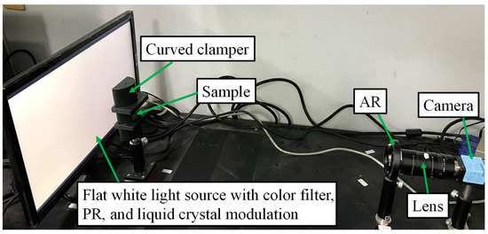
Figure 3.
Instrument configuration of the phase retardation measurements of the test sample under a curving with a 50-mm radius by common-path optical interferometry.
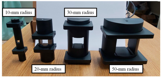
Figure 4.
Curved clampers of 10-, 20-, 30-, and 50-mm radii based on a measurement area of 10 × 10 mm or greater.
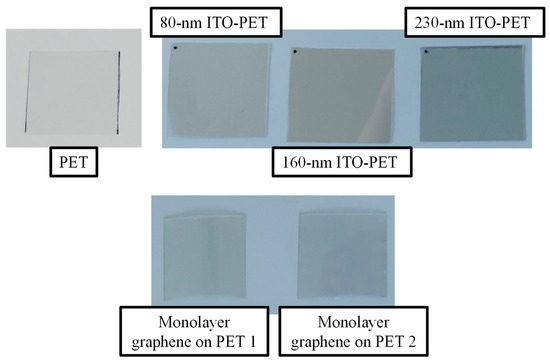
Figure 5.
Photos of 4 × 4 cm PET substrate and transparent conductive films coated on PETs.
This study did not use optical-retardation, quarter-wave, or half-ware plates to calibrate the optical retardation measurements using common-path optical interferometry. The average measurement value in a 10 × 10 mm area was calculated based on 10 measurements. The relationship equation between values of measurement and calibrated optical retardation based on common-path optical interferometry could be obtained using a least-square fitting algorithm [47] as
To analyze the mechanical characteristics of the transparent conductive film-coated PET substrates under curving, an ASTP [42] was used to conduct a whole-folding test. The ASTP controlled the screw mechanism to enable the stage to move back and forth during the whole-folding test of the entire sample up to a 5-mm folding radius, as shown in Figure 6. In addition, a whole-folding test based on a conducting-film layer outward in tension was used to conduct the whole-folding test. Figure 6 depicts a whole-folding test cycle based on a 5-mm folding radius using ASTP.
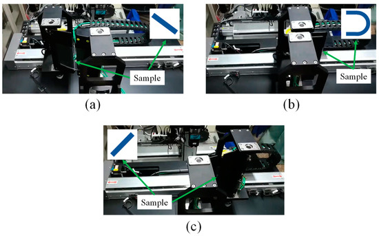
Figure 6.
Schematic of (a–c), (a,b) (in that order) within one whole-folding cycle based on a 5-mm folding radius by ASTP.
4. Experimental Results and Discussion
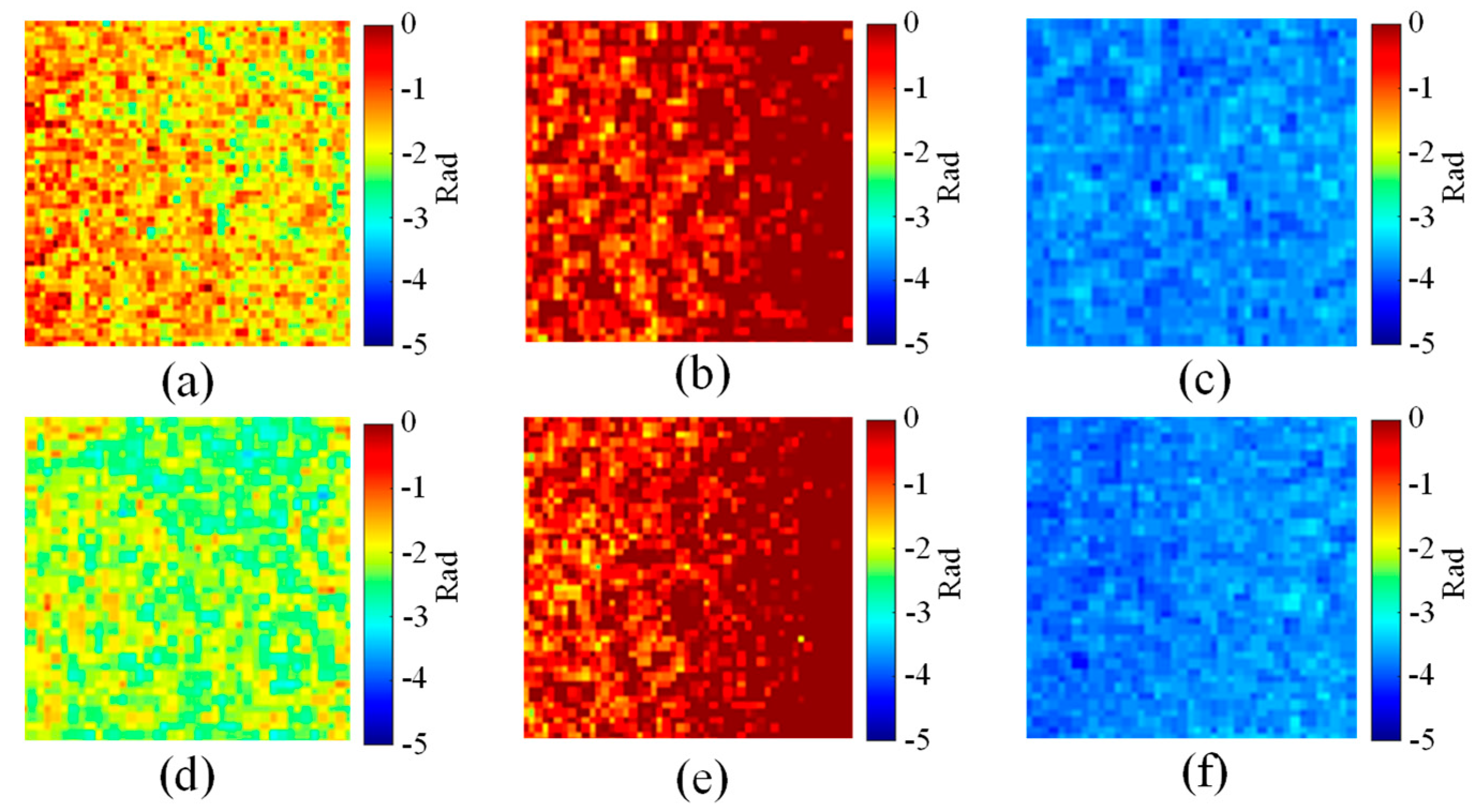
Figure 7 and Table 1 show the phase retardation measurement results of a 125-μm-thick PET substrate under the curving conditions of 50-, 30-, 20-, and 10-mm radii using common-path optical interferometry. The negative value of phase retardation was the result of compressive stress. As Table 1 shows, as the radius of curvature decreased, the phase retardation decreased due to greater compressive stress. This study also measured the phase retardations of 80-, 160-, and 230-nm ITO films coated on 40 × 40 mm 125-μm-thick PET substrates under outer and inner curving conditions of 50-, 30-, 20-, and 10-mm radii before and after 11,000 whole-folding cycles based on a 10-mm folding radius using common-path optical interferometry, as shown in Table 2. As Table 1 and Table 2 show, after ITO was coated on PET, its phase retardation was greater than that of uncoated PET under the same curving conditions. This was particularly the case with 80- and 160-nm ITO-coated PETs. It can be inferred that because the Young’s coefficient (116 GPa [48]) of ITO is much greater than that of PET (4.1 GPa [49]), this caused the ITO film to bend, thereby reducing the bending compressive stress [50]. For the same reason, the phase retardations of ITO-coated PETs under ITO-film inner curving conditions were greater than those under outer curving conditions. However, compared with the other two films, because of the thicker ITO film, the phase retardation of the 230-nm ITO-coated PET was slightly less than that of the uncoated PET. Table 2 shows that the phase retardations of the 160- and 230-nm ITO-coated PETs were the largest and smallest of the three films under different curving conditions, respectively, prior to the 11,000 whole-folding-cycle test. This was because the manufacturing process parameters caused residual stress in the ITO film-coated PET and produced a large or small value of phase retardation in the test sample [50]. In addition, compared to the results before and after the 11,000 whole-folding-cycle test, the phase retardations were not significantly different under the outer and inner curving conditions of 50-, 30-, and 20-mm radii. Nevertheless, the phase retardations of 80-, 160-, and 230-nm ITO films coated on 125-μm-thick PET substrates under outer and inner curving conditions of a 10-mm radius after an 11,000 whole-folding-cycle test were smaller than those prior to the test, as shown in Table 2. Figure 8 and Figure 9 show the phase retardation measurement images of 80-, 160-, and 230-nm ITO films coated on 125-μm-thick PET substrates under a 10-mm radius condition before and after the 11,000 whole-folding-cycle test using common-path optical interferometry. Table 2 shows that the changes in phase retardation of the 160- and 230-nm ITO-coated PETs before and after the test were the largest and smallest, respectively, of the three films under a 10-mm radius condition. The results suggest that the curved-mechanical characteristics of the 160- and 230-nm ITO-coated PET were the worst and best of the three ITO film-coated PETs due to the manufacturing process parameters caused residual stress in the ITO film-coated PET.
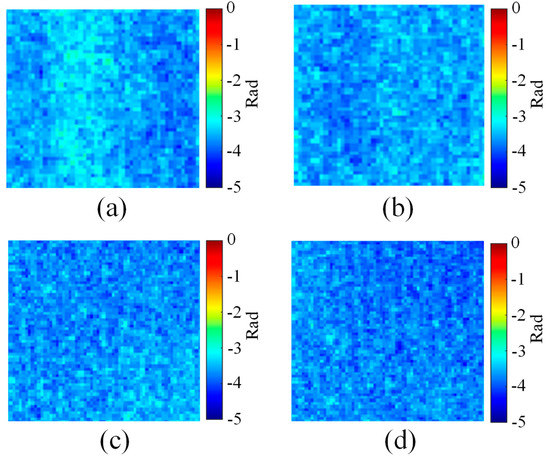
Figure 7.
Phase retardation measurement images of a PET substrate under the curving conditions of (a) 50-, (b) 30-, (c) 20-, and (d) 10-mm radii using common-path optical interferometry.

Table 1.
Phase retardation measurement results of a 125-μm-thick PET substrate under the curving conditions of 50-, 30-, 20-, and 10-mm radii using common-path optical interferometry.

Table 2.
Phase retardation measurements of 80-, 160-, and 230-nm ITO films coated on 40 × 40 mm 125-μm-thick PET substrates under the curving conditions of 50-, 30-, 20-, and 10-mm radii before and after 11,000 whole-folding cycles based on a 10-mm folding radius using common-path optical interferometry.
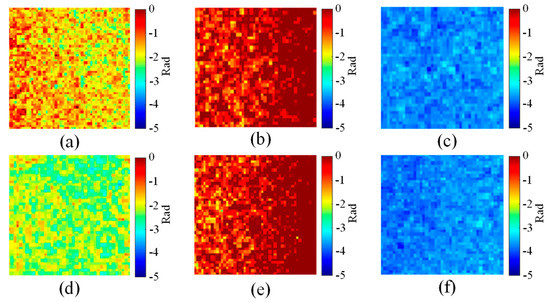
Figure 8.
Phase retardation measurement images of (a,d) 80-, (b,e) 160-, and (c,f) 230-nm ITO films coated on 125-μm-thick PET substrates under (a–c) outer and (d–f) inner curving conditions of a 10-mm radius before the 11,000 whole-folding-cycle test using common-path optical interferometry.
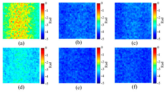
Figure 9.
Phase retardation measurement images of (a,d) 80-, (b,e) 160-, and (c,f) 230-nm ITO films coated on 125-μm-thick PET substrates under (a–c) outer and (d–f) inner curving conditions of a 10-mm radius after the 11,000 whole-folding-cycle test using common-path optical interferometry.
This study also measured the phase retardation of two monolayer graphene films coated on 40 × 40 mm 250-μm-thick PET substrates under the curving conditions of 50-, 30-, 20-, and 10-mm radii before and after 11,000 whole-folding cycles based on a 10-mm folding radius using common-path optical interferometry, as shown in Table 3. As Table 3 shows, because the Young’s coefficient of monolayer graphene (1 TPa [51]) is much greater than that of PET, the phase retardations of monolayer-graphene-coated PETs under graphene-film inner curving conditions were greater than those under outer curving conditions, which caused the monolayer graphene film to bend, thereby reducing the bending compressive stress [50]. In addition, the phase retardations of monolayer graphene on the first PET sample (graphene/PET 1) under the inner curving conditions before 11,000 whole-folding cycles based on a 10-mm folding radius were obviously greater than those after the test by approximately 1 rad. The results suggest that there was a residual compressive stress in graphene/PET 1 that was the direct result of the manufacturing process parameters. For monolayer graphene on the second sample (graphene/PET 2), the phase retardations were not significantly different under the same conditions before and after the 11,000 whole-folding-cycle test. Nevertheless, the phase retardations of graphene/PET 2 under outer and inner curving conditions of the 10-mm radius after the 11,000 whole-folding-cycle test were smaller than those before by approximately 1.5 rad. The results suggest that a compressive residual stress in the graphene/PET 2 was induced under the same conditions of the 10-mm radius before the 11,000 whole-folding-cycle test. After the 11,000 whole-folding-cycle test, a compressive residual stress in the graphene/PET 2 was released. The results suggest that the curved-mechanical characteristics of the graphene/PET 2 were better than graphene/PET 1, due to the manufacturing process parameters causing less residual stress in the monolayer graphene film-coated PET.

Table 3.
Phase retardation measurements of monolayer graphene 1 and 2 films coated on 40 × 40 mm 250-μm-thick PET substrates under curving conditions of 50-, 30-, 20-, and 10-mm radii before and after 11,000 whole-folding cycles based on a 10-mm folding radius using common-path optical interferometry.
5. Conclusions
This study presented a method for measuring the curved-mechanical characteristics of transparent conductive film-coated polymer substrates using common-path optical interferometry. To analyze the mechanical characteristics of the transparent conductive film-coated PET substrates under curving, this study utilized an ASTP for a whole-folding test. The study then investigated and analyzed 80-, 160-, and 230-nm ITO films coated on 40 × 40 mm 125-μm-thick PET substrates and monolayer graphene films coated on 40 × 40 mm 250-μm-thick PET substrates under the curving conditions of 50-, 30-, 20-, and 10-mm radii before and after an 11,000 whole-folding cycle test based on a 10-mm folding radius. Experimental results revealed that the curved-mechanical characteristics of the 160- and 230-nm ITO-coated PET were the worst and best of the three ITO film-coated PETs, due to the manufacturing process parameters causing residual stress in the ITO film-coated PET. In addition, residual compressive stresses were observed in the graphene/PET 1 and PET 2 samples. The results suggest that the curved-mechanical characteristics of the graphene/PET 2 were better than graphene/PET 1, due to the manufacturing process parameters causing less residual stress in the monolayer graphene film-coated PET. The results of the curved-mechanical characteristic measurements of flexible transparent conductive substrates can provide designers with improved product development or assist manufacturers in improving the manufacturing design of enhanced coating processes.
Author Contributions
Methodology, B.-J.W.; software, B.-J.W. and J.-J.H.; validation, B.-J.W. and J.-J.H.; formal analysis, B.-J.W. and J.-J.H.; investigation, B.-J.W.; resources, B.-J.W.; data curation, B.-J.W.; writing—original draft preparation, B.-J.W.; writing—review and editing, B.-J.W.; visualization, B.-J.W.; supervision, B.-J.W. All authors have read and agreed to the published version of the manuscript.
Funding
The authors wish to thank National Science Council of Taiwan for financial support (Grant No.: 108–2221-E−019–056).
Conflicts of Interest
The authors declare no conflict of interest.
References
- Alqadami, A.S.M.; Jamlos, M.F.; Soh, P.J.; Kamarudin, M.R. Polymer (PDMS-Fe3O4) magneto-dielectric substrate for a MIMO antenna array. Appl. Phys. A 2016, 122, 9. [Google Scholar] [CrossRef]
- Economou, A.; Kokkinos, C.; Prodromidis, M. (Mamas) Flexible plastic, paper and textile lab-on-a chip platforms for electrochemical biosensing. Lab Chip 2018, 18, 1812–1830. [Google Scholar] [CrossRef] [PubMed]
- Chaudhary, K.; Singh, G.; Ramkumar, J.; Ramakrishna, S.A.; Srivastava, K.V.; Ramamurthy, P.C. Optically Transparent Protective Coating for ITO-Coated PET-Based Microwave Metamaterial Absorbers. IEEE Trans. Compon. Packag. Manuf. Technol. 2020, 10, 378–388. [Google Scholar] [CrossRef]
- Charmet, J.; Rodrigues, R.; Yildirim, E.; Challa, P.K.; Roberts, B.; Dallmann, R.; Whulanza, Y. Low-Cost Microfabrication Tool Box. Micromachines 2020, 11, 135. [Google Scholar] [CrossRef] [PubMed] [Green Version]
- Elakkiya, A.; Radha, S.; Sreeja, B.S.; Manikandan, E. Terahertz broadband metamaterial absorber enabled by SiO2SiO2, polyimide and PET dielectric substrates. Pramana 2020, 94, 1–6. [Google Scholar] [CrossRef]
- Li, H.; Dong, W.; Wu, X.; Xi, J.; Ji, Z. Resistive switching characteristics of ZnO/a-TiO2 bilayer film fabricated on PET/ITO transparent and flexible substrates. Mater. Res. Bull. 2016, 84, 449–454. [Google Scholar] [CrossRef]
- Kim, T.H.; Park, S.H.; Kim, D.H.; Nah, Y.C.; Kim, H.K. Roll-to-roll sputtered ITO/Ag/ITO multilayers for highly transparent and flexible electrochromic applications. Sol. Energy Mater. Sol. Cells 2017, 160, 203–210. [Google Scholar] [CrossRef]
- Shekargoftar, M.; Krumpolec, R.; Homola, T. Enhancement of electrical properties of flexible ITO/PET by atmospheric pressure roll-to-roll plasma. Mater. Sci. Semicond. Process. 2018, 75, 95–102. [Google Scholar] [CrossRef]
- Zhang, Y.; Pan, T.; Yang, Z. Flexible polyethylene terephthalate/polyaniline composite paper with bending durability and effective electromagnetic shielding performance. Chem. Eng. J. 2020, 389, 124433. [Google Scholar] [CrossRef]
- Song, W.-L.; Cao, M.-S.; Lu, M.-M.; Bi, S.; Wang, C.-Y.; Liu, J.; Yuan, J.; Fan, L.-Z. Flexible graphene/polymer composite films in sandwich structures for effective electromagnetic interference shielding. Carbon 2014, 66, 67–76. [Google Scholar] [CrossRef]
- Alam, A.; Meng, Q.; Shi, G.; Arabi, S.; Ma, J.; Zhao, N.; Kuan, H.C. Electrically conductive, mechanically robust, pH-sensitive graphene/polymer composite hydrogels. Compos. Sci. Technol. 2016, 127, 119–126. [Google Scholar] [CrossRef]
- Li, A.; Zhang, C.; Zhang, Y.F. Thermal conductivity of graphene-polymer composites: Mechanisms, properties, and applications. Polymers 2017, 9, 437. [Google Scholar]
- Kumari, S.; Panigrahi, A.; Singh, S.K.; Pradhan, S.K. Enhanced corrosion resistance and mechanical properties of nanostructured graphene-polymer composite coating on copper by electrophoretic deposition. J. Coat. Technol. Res. 2018, 15, 583–592. [Google Scholar] [CrossRef]
- Zhang, M.; Wang, X.; Yang, T.; Zhang, P.; Wei, X.; Zhang, L.; Li, H. Polyaniline/graphene hybrid fibers as electrodes for flexible supercapacitors. Synth. Met. 2020, 268, 116484. [Google Scholar] [CrossRef]
- Suzuki, T.; Itoh, T.; Vantasin, S.; Minami, S.; Kutsuma, Y.; Ashida, K.; Kaneko, T.; Morisawa, Y.; Miura, T.; Ozaki, Y. Tip-enhanced Raman spectroscopic measurement of stress change in the local domain of epitaxial graphene on the carbon face of 4H-SiC (000–1). Phys. Chem. Chem. Phys. 2014, 16, 20236–20240. [Google Scholar] [CrossRef] [PubMed]
- Mishra, A.; Singh, V.K.; Mohanty, T. Coexistence of interfacial stress and charge transfer in graphene oxide-based magnetic nanocomposites. J. Mater. Sci. 2017, 52, 7677–7687. [Google Scholar] [CrossRef]
- Wang, C.; Wang, J.; Barber, A.H. Stress concentrations in nanoscale defective graphene. AIP Adv. 2017, 7, 115001. [Google Scholar] [CrossRef]
- Young, R.J.; Liu, M.; Kinloch, I.A.; Li, S.; Zhao, X.; Vallés, C.; Papageorgiou, D.G. The mechanics of reinforcement of polymers by graphene nanoplatelets. Compos. Sci. Technol. 2018, 154, 110–116. [Google Scholar] [CrossRef]
- Morgan, J.J.; Craciun, M.F.; Eichhorn, S.J. Quantification of stress transfer in a model cellulose nanocrystal/graphene bilayer using Raman spectroscopy. Compos. Sci. Technol. 2019, 177, 34–40. [Google Scholar] [CrossRef]
- Romero-Vargas Castrillón, S.; Perreault, F.; De Faria, A.F.; Elimelech, M. Interaction of graphene oxide with bacterial cell membranes: Insights from force spectroscopy. Environ. Sci. Technol. Lett. 2015, 2, 112–117. [Google Scholar] [CrossRef]
- Gupta, S.; McDonald, B.; Carrizosa, S.B.; Price, C. Microstructure, residual stress, and intermolecular force distribution maps of graphene/polymer hybrid composites: Nanoscale morphology-promoted synergistic effects. Compos. Part B Eng. 2016, 92, 175–192. [Google Scholar] [CrossRef]
- Li, Z.; Young, R.J.; Papageorgiou, D.G.; Kinloch, I.A.; Zhao, X.; Yang, C.; Hao, S. Interfacial stress transfer in strain engineered wrinkled and folded graphene. 2D Mater. 2019, 6, 045026. [Google Scholar] [CrossRef]
- Wen, B.J.; Liu, T.S. Edge contrast failure analysis on vision angle of human eyes for curve displays. J. Disp. Technol. 2012, 8, 418–423. [Google Scholar] [CrossRef]
- Sinitski, E.H.; Thompson, A.A.; Godsell, P.; Honey, J.; Besemann, M. Postural stability and simulator sickness after walking on a treadmill in a virtual environment with a curved display. Displays 2018, 52, 1–7. [Google Scholar] [CrossRef]
- Kim, Y.G.; Han, K.Y. Spread characteristics of OCR lamination for flexible OLED display process with flat and curved substrates. Jpn. J. Appl. Phys. 2021, 60, 056504. [Google Scholar] [CrossRef]
- Sharpe, W.N. Springer Handbook of Experimental Solid Mechanics; Springer Science & Business Media: Berlin/Heidelberg, Germany, 2008. [Google Scholar]
- Hecht, E. Optics, 4th ed.; Reading; Addison-Wesley: Boston, MA, USA, 2002. [Google Scholar]
- Lee, Y.C.; Liu, T.S.; Wu, C.I.; Lin, W.Y. Investigation on residual stress and stress-optical coefficient for flexible electronics by photoelasticity. Measurement 2012, 45, 311–316. [Google Scholar] [CrossRef]
- Lin, Y.; Zhou, Z.; Wang, R. Optical heterodyne measurement of the phase retardation of a quarter-wave plate. Opt. Lett. 1988, 13, 553–555. [Google Scholar]
- Nakadate, S. High precision retardation measurement using phase detection of Young’s fringes. Appl. Opt. 1990, 29, 242–246. [Google Scholar] [CrossRef]
- Lo, Y.L.; Lai, C.H.; Lin, J.F.; Hsu, P.F. Simultaneous absolute measurements of principle angle and phase retardation with a new common-path heterodyne interferometer. Appl. Opt. 2004, 43, 2013–2022. [Google Scholar] [CrossRef]
- Chen, Y.L.; Su, D.C. Full-field measurement of the phase retardation for birefringent elements by using common path heterodyne interferometry. Opt. Las. Eng. 2009, 47, 484–487. [Google Scholar] [CrossRef]
- Yu, T.C.; Lo, Y.L. A Highly Phase-Sensitive Heterodyne Polariscope for the Full-Field Measurement of Twisted- Nematic Liquid Crystal. IEEE Photonics Technol. Lett. 2008, 20, 1778–1780. [Google Scholar] [CrossRef]
- Chu, Y.C.; Chang, W.Y.; Chen, K.H.; Chen, J.H.; Tsai, B.C.; Hsu, K.Y. Full-field refractive index measurement with simultaneous phase-shift interferometry. Opt. Int. J. Light Electron Opt. 2014, 125, 3307–3310. [Google Scholar] [CrossRef]
- Wen, B.J.; Huang, S.A. Residual stress image inspections based on bending testing for flexible transparent conducting substrates by single-direction common-path image interferometry. IEEE Sens. J. 2018, 19, 1701–1709. [Google Scholar] [CrossRef]
- Aben, H.; Guillemet, C. Photoelasticity of Glass; Springer Science & Business Media: Berlin/Heidelberg, Germany, 2012. [Google Scholar]
- Quiroga, J.A.; Gómez-Pedrero, J.A. Application of principal component analysis in phase-shifting photoelasticity. Opt. Express 2016, 24, 5984–5995. [Google Scholar] [CrossRef] [Green Version]
- Júnior, P.M.; Vieira, F.G.; Magalhães, C.A.; Ribeiro, J.S.; Rios, I.G. Numerical method to digital photoelasticity using plane polariscope. Opt. Express 2016, 24, 12617–12624. [Google Scholar] [CrossRef]
- Probst, A.C.; Begou, T.; Döhring, T.; Zeising, S.; Stollenwerk, M.; Stadtmüller, J.; Emmerich, F.; Lumeau, J. Coating stress analysis and compensation for iridium-based x-ray mirrors. Appl. Opt. 2018, 57, 8775–8779. [Google Scholar] [CrossRef]
- Jena, S.; Tokas, R.B.; Tripathi, S.; Rao, K.D.; Udupa, D.V.; Thakur, S.; Sahoo, N.K. Influence of oxygen partial pressure on microstructure, optical properties, residual stress and laser induced damage threshold of amorphous HfO2 thin films. J. Alloys Compd. 2019, 771, 373–381. [Google Scholar] [CrossRef]
- Pan, L.; Qi, R.; Feng, Y.; Chen, J.; Zhang, Z.; Li, W.; Wang, Z. Effect of nitrogen doping on surface morphology, microstructure, chemical composition and intrinsic stress of nickel thin films deposited by reactive sputtering. Surf. Coat. Technol. 2019, 364, 196–203. [Google Scholar] [CrossRef]
- Wen, B.J.; Huang, S.A.; Tseng, T.Y. Experimental analysis of interfacial shear stress and electrical resistance of indium tin oxide-coated polyethylene terephthalate films for a whole folding test. J. Plast. Film Sheeting 2020, 36, 130–150. [Google Scholar] [CrossRef]
- Medhat, M.; Hendawy, N.I.; Zaki, A.A. Fringes of equal tangential inclination by curvature-induced birefringence. Opt. Laser Technol. 2003, 35, 31–35. [Google Scholar] [CrossRef]
- Wen, B.J.; Hsu, J.S.; Liu, W.C. Two-dimension phase-retardation distribution inspections for flexible displays by using full-field liquid-crystal modulating common-path interferometry. Jpn. J. Appl. Phys. 2014, 53, 05HB03. [Google Scholar] [CrossRef]
- Ghiglia, D.C.; Pritt, M.D. Two-Dimensional Phase Unwrapping: Theory, Algorithms, and Software; Wiley: New York, NY, USA, 1998. [Google Scholar]
- Malacara, D. Optical Shop Testing; John Wiley & Sons Inc.: Hoboken, NJ, USA, 2007. [Google Scholar]
- IEEE. Standard for Terminology and Test Methods for Analog-to-Digital Converters; IEEE Std. 1241-2000; IEEE: Piscataway, NJ, USA, 2000; pp. 25–29. [Google Scholar]
- Neerinck, D.G.; Vink, T.J. Depth profiling of thin ITO films by grazing incidence X-ray diffraction. Thin Solid Films 1996, 278, 12–17. [Google Scholar] [CrossRef]
- Lagazzo, A.; Moliner, C.; Bosio, B.; Botter, R.; Arato, E. Evaluation of the mechanical and thermal properties decay of PHBV/sisal and PLA/sisal biocomposites at different recycle steps. Polymers 2019, 11, 1477. [Google Scholar] [CrossRef] [PubMed] [Green Version]
- Gere, J.M.; Timoshenko, S.P. Mechanics of Materials; PWS-KENT Publishing Company: Boston, MA, USA, 1997. [Google Scholar]
- Cao, Q.; Geng, X.; Wang, H.; Wang, P.; Liu, A.; Lan, Y.; Peng, Q. A review of current development of graphene mechanics. Crystals 2018, 8, 357. [Google Scholar] [CrossRef] [Green Version]
Publisher’s Note: MDPI stays neutral with regard to jurisdictional claims in published maps and institutional affiliations. |
© 2021 by the authors. Licensee MDPI, Basel, Switzerland. This article is an open access article distributed under the terms and conditions of the Creative Commons Attribution (CC BY) license (https://creativecommons.org/licenses/by/4.0/).


