Abstract
An environmentally friendlier solution processing has been introduced to fabricate zirconium oxide (ZrO2) films on quartz substrates, using spin coating of simple water-based solution. The films cured with UV-A = 330 nm for different times (40, 80, 120 min) were investigated for structural and optical properties and compared with thermally annealed film (at 350 °C). XRD and Raman spectroscopy showed amorphous structure in all the samples with no significant phase transformation with UV-A exposure. AFM microscopy showed smooth and crack free films with surface roughness ≤2 nm that reduced with UV-A exposure. Ultraviolet-visible (UV–Vis) spectroscopy demonstrated optical transmittance ≥88% and energy band gap variations as 4.52–4.70 eV. Optical constants were found from spectroscopic ellipsometry (SE). The refractive index (n) values, measured at 470 nm increased from 1.73 to 2.74 as the UV-A exposure prolonged indicating densification and decreasing porosity of the films. The extinction coefficient k decreased from 0.32 to 0.19 indicating reduced optical losses in the films under the UV-A exposure. The photoluminescence (PL) spectra exhibited more pronounced UV emissions which grew intense with UV-A exposure thereby improving the film quality. It is concluded that UV-A irradiation can significantly enhance the optical properties of ZrO2 films with minimal changes induced in the structure as compared to thermally treated film. Moreover, the present work indicates that water-based solution processing has the potential to produce high-quality ZrO2 films for low cost and environmental friendlier technologies. The work also highlights the use of UV-A radiations as an alternate to high temperature thermal annealing for improved quality.
Keywords:
water; solution processing; ZrO2; UV-A treatment; amorphous; transparent; optical properties 1. Introduction
Zirconia (ZrO2) has emerged as an excellent material due to its unique properties such as wide band gap (3–7.8 eV) [1,2], high level stability (chemical, thermal, and electrical), tuneable conductivity, and high refractive index, making it suitable for high performance bio medical [3], sensing [4,5], catalyst [6] and many more applications. Most important of all, its high dielectric constant has rendered it an ultimate position as a viable substitute for conventional gate dielectric in transistors [7,8] and in storage capacitors [9], for future generation electronic technologies.
The synthesis of ZrO2 has been carried out with a variety of techniques based on both vacuum and solution processing [3,10,11,12]. However, the key point is that tailor-made properties of ZrO2 thin films can be achieved with the right choice of various factors, in both pre- and post-deposition procedures. For example, the degree of crystallinity in oxidized films governs not only dielectric properties but ionic conductivity, and mechanical strength as well [13,14], which can be controlled with post deposition heat treatment [12,15,16]. Therefore, different authors have investigated thermal treatment [12,17,18] for the vital role it plays in producing optimal properties of ZrO2 films needed for a range of applications. High temperature annealing is used to improve the crystallinity of films and make these more uniform. However, in oxide films like in the present case, this also results in the loss of oxygen and non-uniformity of films. In recent years, a different approach that can decrease the curing temperature of solution-processed oxide films and improve the properties, has been developed and has gained increasing interest because the modern era of technology is heading towards transparent and flexible applications which require low temperature processing. Therefore the paradigm of heat treatment has changed in due course of its development to low temperature annealing [15] and even better the ultraviolet (UV)/photo annealing [10,11,16,17]. Here, the latter approach has emerged as a promising alternative to high temperature treatments because the film surface can be directly processed, without heating, using appropriate energy of light which can enhance the ionic diffusion in the oxide films as well [18]. Furthermore, UV radiation exposure of films is done to improve the bonding of films and thus it is assumed that no oxygen will be lost during the exposure.
The UV spectrum (100−400 nm) is categorized into three groups known as UV-A (320−400 nm), UV-B (290−320 nm), and UV-C (100−290 nm). The mechanism of UV irradiation has been studied for ZrO2 films using wavelengths of 185 nm and 254 nm [10,19] that fall in the category of UV-C. The wavelengths are comparable to oxygen molecule bond energies and therefore can induce oxygen radicals and ozone [19] which, due to the low activation energy, further give boost to the oxidation rate [11]. This mechanism has been used to lower the deposition temperature and activate oxidation to process the films. For example, Liu et al. [20] demonstrated that UV-treated ZrO2 films can produce high performance properties, such as low leakage current, large areal capacitance, and smoother surfaces as compared to thermally treated films. More studies include dielectric and electric properties [11,16,21] of UV treated ZrO2 films for TFT applications. Desforges et al. [10] studied the Ketteler–Helmholtz dispersion relations to determine the optical properties of UV irradiated ZrO2 thin films from a single transmittance curve and also observed reduction in surface roughness of these films. However, there are quite a few reports which have employed high wavelength side of the UV spectrum to investigate the induced changes. These studies include UV ~330 nm treatment on zinc oxide ZnO-based transistors [22], on gadolinium Gd-doped ZrO2 films [16] and the biological studies of UV ~365 nm treated ZrO2 films [17]. The purpose of this study was not only to investigate the impact of UV-A (320–400 nm) exposure on ZrO2 films’ structural and optical properties but also use solution processing which does not pose any threat to the environment and also does not rely on cumbersome procedures involved in sol-gel method. Our group has recently reported high performance Y-doped ZnO films fabricated by water-based solution without the need to prepare sol-gel [23] and we have applied the same approach for fabrication of ZrO2 thin films, in this report. The water soluble precursors allow film formation at low temperatures in contrast to the organometallic precursors generally used in solution processing. Moreover, the organometallic precursors produce toxic residues harmful for the environment; water-based solution processing is safe, toxic free and therefore eco-friendly.
In this study, we investigate the effect of photo functionalization by UV-A irradiation on the ZrO2 thin films fabricated by water-based solution processing (no sol-gel). We compare results obtained from UV-A irradiation performed at various amounts of time with those obtained from thermally annealed film and study how differently the time of exposure can affect the structural and optical properties of the films.
2. Materials and Methods
The ZrO2 thin films were deposited by spin coating technique, which uses 0.3 M solution made from zirconium oxychloride octa hydrate (ZrOCl2 8H2O) precursor (purchased from Sigma Aldrich, St. Louis, MO, USA) and deionized (DI) water, without using any catalytic agent. The mixture was magnetically stirred at 50 °C in air for one hour into a transparent and homogenous solution and then aged for one day. The 20 × 20 mm2 sized quartz substrates (double side polished) were cleaned thoroughly, following the standard procedures, in acetone and IPA, using ultrasonic bath at 60 °C for 30 min each. Prior to deposition, the solution was filtered through 0.22 μm PTFE syringe filters and the substrates were washed again with DI water and dried off with a nitrogen gun. The resulting solution was spun coated onto the substrate at the rate of 500 rpm for 6 s and then at 3200 rpm for 30 s, using SÜSS Micro Tec Lithography GmbH spin coater. This coating step was repeated four times in between with a baking step performed at 200 °C for 10 min in air. After deposition, the UV-A exposure was carried out inside a clean chamber equipped with a custom Hg lamp emitting a wavelength of 330 nm and a fan, to maintain the temperature of the chamber. Since the amount of dose is important in such exposures, which can be varied either by varying the time of exposure or by increasing the intensity. In our experiment, since we exposed with constant power lamp, therefore the dose was varied by changing the time of exposure. The UV-A exposure time was varied as 40, 80, and 120 min. The power of the lamp used was 15W and it was kept at a distance of 15 cm from the sample. The intensity of the lamp at sample was 50 W/m2, calculated using the inverse square law. In order to compare the effect of UV-A treatment with thermally treated film, another sample was annealed in air at 350 °C, for one hour. From now on, thermally treated and UV-A treated (40, 80, and 120 min) ZrO2 samples will be referred to as Z-TA, Z-40, Z-80, and Z-120, respectively. The films were then analyzed for changes in structure, surface morphology, and optical properties, induced by thermal as well as UV-A treatment.
The grazing incidence X-ray diffraction using ARL EQUINOX 3000 X-ray diffractometer was performed to evaluate film crystallinity. Raman spectra were recorded, at room temperature, using Dongwoo Optron MST-4000A Raman Spectrometer with a He-Cd Laser (λ = 442 nm), equipped with an air-cooled charge coupled device (CCD). The surface morphology was determined by atomic force microscopy (AFM) in a non-contact mode. All the scans were taken in air using the instrument Alphcontec over an area of 5 × 5 µm2 per scan. AFM measurements were carried out on all the samples of ZrO2 films to investigate the surface morphology and root mean square (RMS) roughness; the latter was estimated using the Gwyddion software. Transmittance spectra were obtained from an instrument named as Hitachi U 4100 UV/VIS spectrophotometer, in the wavelength range of 200 nm to 800 nm. The spectroscopic ellipsometer from (J. A. Woollam Co., Lincoln, NE, USA) was used to determine the film thickness and optical constants such as refractive index, extinction coefficient, and dielectric constant. PL spectra were obtained, at room temperature, using Dongwoo Optron Lab Ram III spectrometer in the wavelength range of 350–730 nm using 325 nm excitation wavelength of He-Cd laser. All the spectra were detector response corrected and analyzed by using Origin 2018 64 bit.
3. Results and Discussion
3.1. Study of Structure and Surface Morphology of UV-A Exposed ZrO2 Films
3.1.1. XRD Analysis
Figure 1 shows the XRD pattern obtained for all the samples based on ZrO2 thin films. We do not observe any crystallization peak in the XRD pattern of ZrO2 film whether it is treated thermally (Z-TA) or with UV-A, moreover appearance of a broad hump/band approves that all the films are amorphous. This observation is supported by the known finding that the ZrO2 films processed at ≤350° exhibit an amorphous phase [12] and also agrees with previous reports demonstrating non-crystalline phase of ZrO2 for annealing temperatures of 250 °C and 350 °C [24] contrary to the crystalline phases observed at ≥450 °C [12,21].
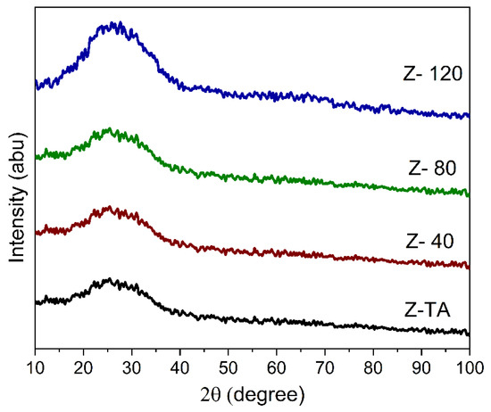
Figure 1.
XRD pattern obtained for all the samples show a broad band indicating amorphous phase. No significant change in the structure of ZrO2 films is observed, whether treated thermally or with UV-A radiation.
Moreover, it is clear from Figure 1 that all the patterns appear in the same form and no distinct diffraction peaks are further added with the UV-A treatment thereby indicating that structural phase is not affected by the treatment. Nonetheless, it is to be noted that the hump is centered at 2θ~25°, which corresponds to monoclinic -ZrO2 reflections (011) and (110) [25,26] and therefore demonstrates that the short range order may be emerging towards the monoclinic [27] phase as indicated by the rise in the hump’s intensity with prolonged UV-A exposure, which on the other hand allows the ZrO2 films to maintain the amorphous structure. Change in crystallinity may be observed if UV-A treatment is stretched further for longer time; this is supported by an earlier finding [19] whereby change in ZrO2 crystallinity was observed after 2 h long exposure of UV radiation.
3.1.2. Study of Raman Spectra
Raman spectroscopy has become a benchmark technique for the identification of the multiple crystalline phases through the signature phonon modes (determined from the group theory). It is now known, for example, that the modes observed at 150, 260, 465, 640 cm−1 [28] represent the tetragonal phase and those occurring at 174, 180, 190, 335, 380, 475, 525, 548, 635 cm−1 [28,29] identify the characteristics of the monoclinic phase of ZrO2. However, these modes smear to a continuum due to structural disorders indicating the amorphous phase [30].
In this study, Raman spectra obtained for all the samples were background subtracted and fitted with Lorentz distribution with the least square best fit in order to identify the phonon modes present as peaks/bands in the spectra. These are shown in Figure 2a, and we observe that all of the spectra are devoid of various peaks that can point to the specific structural phase of the studied films. Moreover, we do not observe any substantial variation of the spectral shape and emergence of new bands in the measured region for any sample which has been exposed to UV-A radiation. Therefore, all the spectra largely represent the amorphous phase, in agreement with XRD results. Nonetheless, we can see the emergence of only one peak centered at 181 cm−1 characteristics of the monoclinic phase which is actually identified with 18 theoretically calculated phonon modes [31]. Therefore, it is justifiable to establish that the ZrO2 thin films when treated thermally or with UV-A radiation demonstrate an amorphous phase. However, to clarify the changes induced by the UV-A treatment, Figure 2b shows the results for intensity and full width at half maximum (FWHM) of the only peak observed in the Raman spectra. We can observe that UV-A treatment has resulted in increased intensity and reduced FWHM (36.1 to 27.7 cm−1) as the treatment time was prolonged, when compared with thermally treated sample. Hence, we suggest that although UV-A treatment did not restructure the lattice and all the films exhibited amorphous phase, there is a tinge of monoclinic order which improves as the treatment is prolonged and may emerge if the films were studied for a further increase in the UV-A exposure time, for future studies.
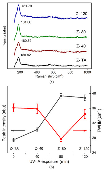
Figure 2.
(a) Raman spectra are shown for thermally annealed and UV-A treated ZrO2 films. The films appear amorphous as no characteristic phonon modes required to represent the crystalline phase are identifiable except for one mode around 180 cm−1 that belongs to one of the 18 mode of monoclinic phase. Nonetheless, UV-A treatment has caused an improvement in this mode with prolonged exposure as depicted in (b) by the intensity and full width at half maximum (FWHM).
3.1.3. Study of AFM Images
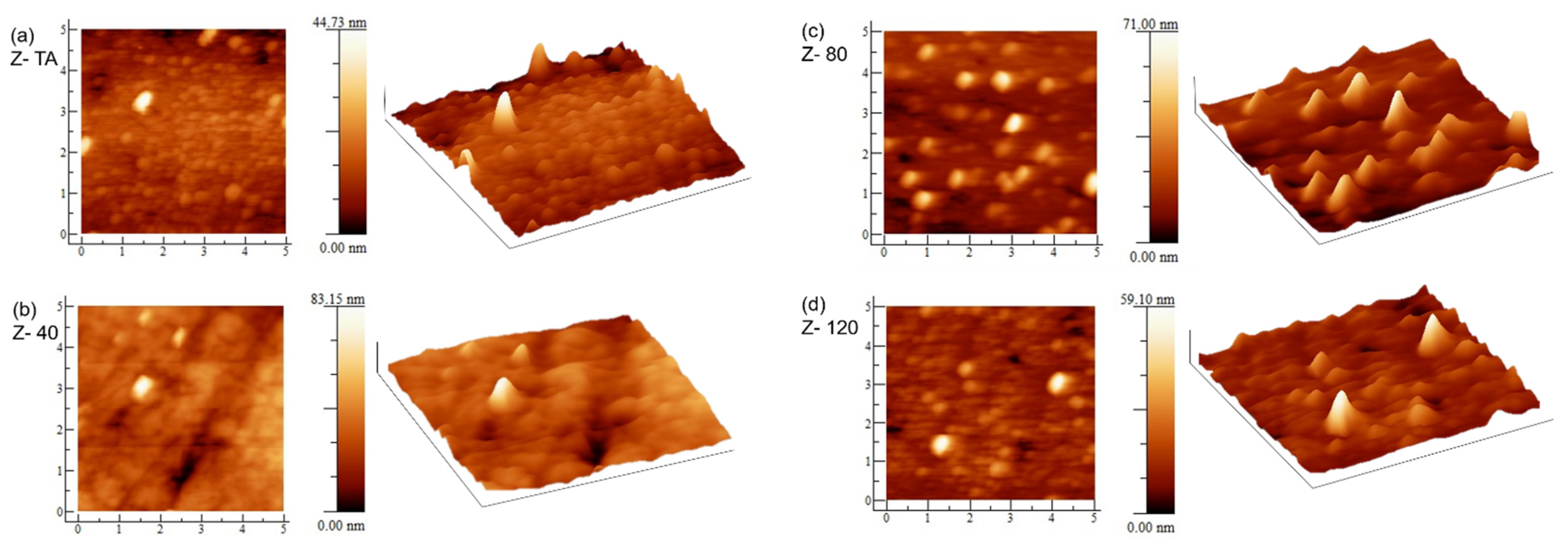
To explore the effect of the UV-A treatment on the surface morphology of the ZrO2 thin films, AFM measurements were performed. The visual appearance and surface roughness obtained in this measurement can quantitatively analyze the morphology and the microstructure which play an important role for future applications. The 2D and 3D images are shown in Figure 3, for all the samples. The effect of UV-A treatment, in terms of grain growth, on surface morphology can be seen. The sample Z- TA, with thermal treatment, shows the presence of large number of tiny grains uniformly distributed over the area. The sample Z- 40, treated for 40 min under UV-A, clearly represents an overall homogeneous and smoother surface with uniformly dispersed grains over all the scanned area. With increase in UV-A treatment time, we observe changes further to the grain’s distribution and their size. Since the cation diffusion across the grain boundaries governs the grain growth, we can speculate that UV-A radiation has affected the phenomena linked with cation kinetics; whereas, anion migration is reflected when there is no significant grain growth which has also been observed previously in UV irradiated ZrO2 films [19].
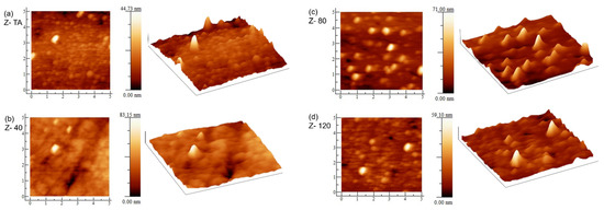
Figure 3.
AFM images (2D and 3D) of (a) thermally annealed ZrO2 film Z- TA and (b–d) UV-A treated ZrO2 films Z40, Z80, and Z120. Change in surface morphology, with UV-A exposure time, is clear. The lengths of the sides in each image are 5 µm.
The root mean square (RMS) roughness was evaluated and is given in Table 1. This indicates that all the films are fairly smooth with roughness values ≤2 nm. This is promising since the high-quality interface with the channel layer demands a smooth surface having small roughness of the dielectric which can enhance the operation of the TFT device considerably [32]. Moreover, the decrease in roughness with UV-A treatment points that UV treatment is capable to reduce the organic residues due to the oxygen radicals [33] and has the potential to substitute thermal annealing process. A similar trend in roughness has been observed in earlier studies [10,34] in ZrO2 films irradiated by UV = 230 nm. The change in roughness can be due to the changes linked with grains’ configuration and structure densification that may occur in the due course of processes that take place because of UV-A treatment of the films [35,36]. The latter (structure densification) has been confirmed from an increase in refractive index n, in these films with UV-A exposure (presented later). Most importantly, the surface morphology obtained using this low cost and environmentally friendlier technique indicates fairly smooth surfaces which validate the appropriateness of this method for device applications of these films.

Table 1.
Physical and optical parameters obtained for thermally treated and UV-A treated ZrO2 thin films.
3.2. Optical Properties
3.2.1. UV–Vis Analysis
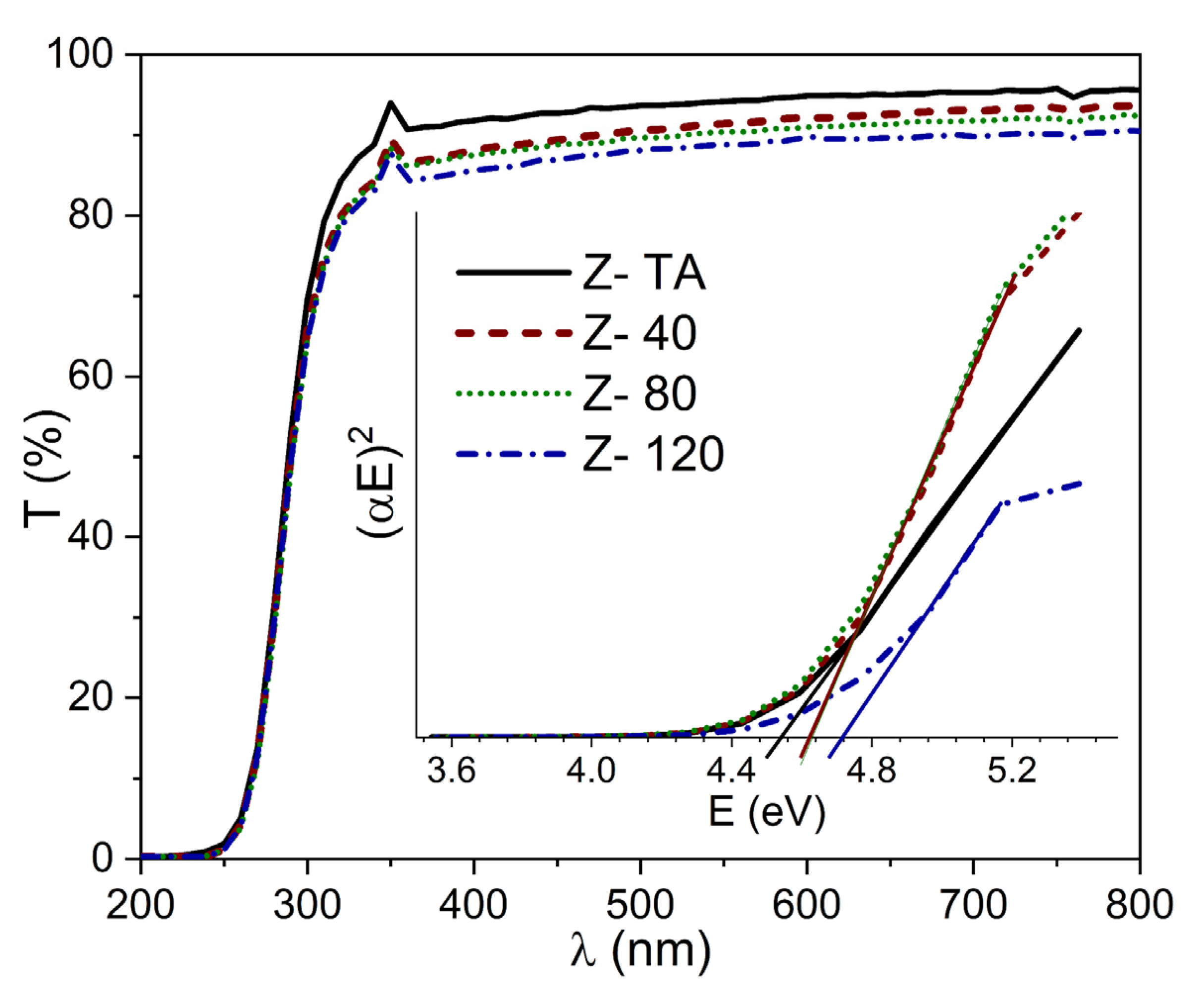
The optical transmittance spectra (T) of thermally treated ZrO2 and UV-A treated ZrO2 thin films (40, 80, and 120 min) deposited on glass substrates are shown in Figure 4. The average transmittance calculated in the spectral region (200–800 nm) demonstrate the value above 88%, given in Table 1, indicating high transparency revealing homogeneity and chemical purity of all the film samples. All the spectra show an absolute absence of interference fringes thereby ruling out multiple reflections that may occur at the interfaces irrespective of the UV-A treatment and indicate that all the films are homogeneously thin. This further signifies that maximum light entered has been transmitted [37], thereby making these films aptly suitable for optical applications. Moreover, as the time for UV-A treatment is increased from 40 to 120 min, we observe a decrease in the transmittance which can be attributed to the change in surface morphology of these films or the removal of the oxygen impurities with long UV-A exposure. Most importantly, it is in agreement with work reported by Xin Dong and co-workers [11] for spin-coated ZrO2 films exposed to UV. Although it is contrary to the increase in transmittance previously reported for UV irradiated ZrO2 films produced by magnetron sputtering [10]. However, thermal annealing has also been observed to decrease the transmittance of sol-gel derived ZrO2 films [38]. Therefore, we assume that the benefit of these processes in terms of oxidation state of the films is very similar. Nonetheless, since optical properties are also governed by the structural/morphological changes, a well-defined trend observed in transmittance due to these treatments may not be established.
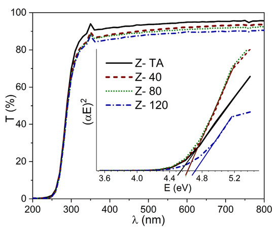
Figure 4.
Transmittance spectra for thermally treated and UV-A treated ZrO2 films indicate highly transparent films. The inset shows the Tauc plots, for all the samples, used to evaluate the energy band gap Eg of these films.
We clearly observe the absorption edge in the transmittance spectra near the UV region which marks the optical band gap Eg of the given film. Although visible shift in this absorption edge with the UV-A treatment cannot be seen which is in agreement with a previously reported UV treated ZrO2 films [10], nonetheless the corresponding Eg does change as found from the Tauc equation given as,
where E is the incident photon energy (eV), A is a constant, and α is the absorption coefficient determined from the following equation.
The thickness (t) of each film was determined from SE measurements and is given in Table 1. We had obtained Tauc plot (a graph between (αE)2 and (E)) and found values of Eg, for thermally treated and UV-A treated ZrO2 films, by extrapolating the linear curve to the (E) axis as shown in the inset of Figure 4. The values for thermally treated ZrO2 and the films with UV-A treatment at 40, 80, and 120 min are 4.52, 4.62, 4.60, and 4.70 eV, respectively. The list of Eg obtained for all the samples is also given in Table 1. The trend observed in this study agrees well with a previous report [11] whereby ZrO2 film was exposed to UV radiation for time variations up to 80 min. It has been established that density of localized band gap states arising due to the defects, impurities, and disorder in the material lattice, is more likely the cause to reduce Eg. On the other hand, the annealing temperature by improving the crystalline quality can be a cause to increase the Eg value [39]. For ZrO2, it has already been reported [40] that both defects and crystal order/disorder intervenes to play a key role in the electronic structure thereby changing the Eg. In our case, it seems plausible to assume that improvement in crystalline quality (confirmed from Raman results) can be held responsible for the observed increase in Eg with UV-A treatment of ZrO2 films. Lastly, it is important to mention that the Eg values found in this study for all the samples agree with previously reported values. It is quite recent that Ibrahim and co-workers [2] produced pure ZrO2 thin films, using impregnation method, with Eg = 4.61 eV and Lopez et al. [12] demonstrated a similar trend in Eg (3.92 eV–4.037 eV) for annealed ZrO2 films. Another interesting observation depicted in Figure 4, is the absence of long tail near the absorption edge observed for all the films. This implies that there were no conduction band edge states which are generally incorporated by impurities during deposition procedures and are attributed to the oxygen vacancies. This again confirms that the deposition procedure adopted is robust and high performance.
3.2.2. Optical Constants from Spectroscopic Ellipsometry (SE)
SE is a valuable technique to measure the optical response of materials in terms of ψ (amplitude) and Δ (phase) of the reflected light and can provide information of the thickness and the optical constants such as refractive index (n), extinction coefficient (k), and dielectric constant (ε) of a multilayer system [41]. The thickness values thus acquired for thermally treated and UV-A treated ZrO2 film samples have been shown in Table 1.
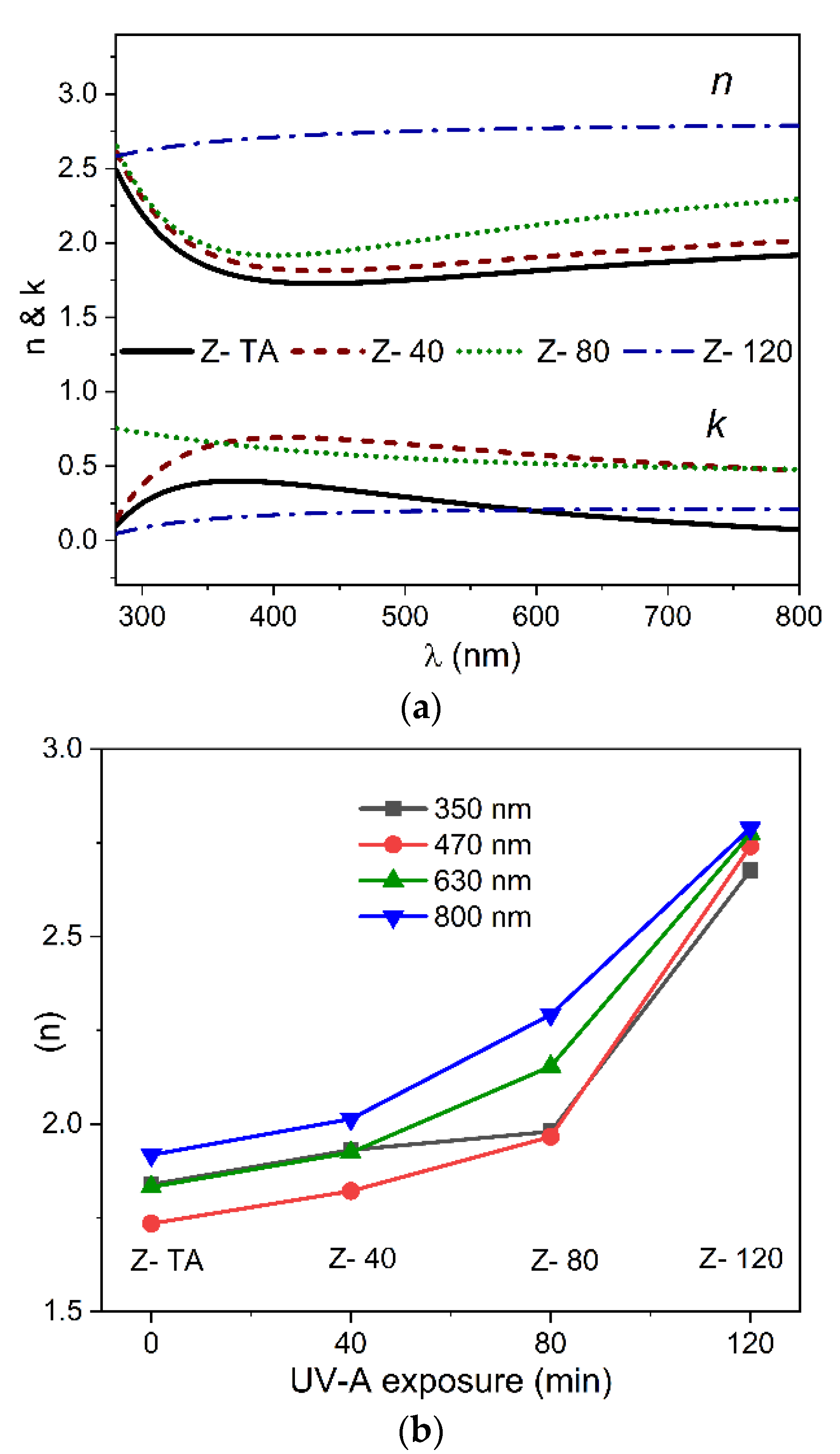
Figure 5a shows the dispersion curves of both n and k in the wavelength range of 280–800 nm and a noticeable change with UV-A treatment as well. The fact that the observed n is less than the value ~2 (normally found out for ZrO2) can be attributed to the amorphous nature of the films and is comparable to the range previously reported for sol-gel derived amorphous ZrO2 thin films [42] and even greater than the value 1.45 reported recently for sol-gel derived polycrystalline ZrO2 thin films [43]. We can observe that an increase in UV-A exposure time produces a progressive increase of the refractive index values to 2.67 from 1.83 observed for thermally treated ZrO2 film, measured at 630 nm, which confirms that UV-A treatment brings an improvement in homogeneity of these films. It is known that refractive index n, in general, is governed by characteristics of the films associated closely with structure and morphology. The former is related with order/disorder configuration, but the latter is mainly correlated with the surface roughness and density of the films. Following the tendency observed in n of the films exposed to UV-A radiation together with the structural studies, we anticipate that the refractive index follows the morphological aspect more than the structural considerations as the UV-A exposure time is increased.
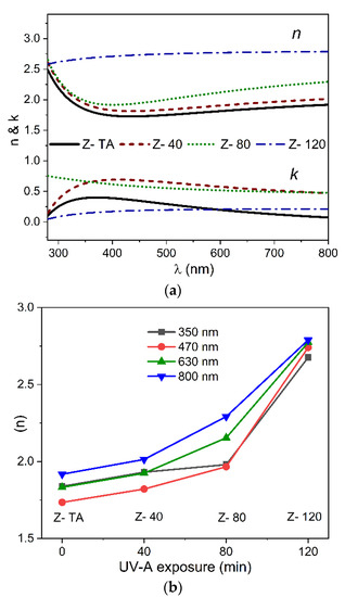
Figure 5.
The dispersion curves of n and k (a) plotted against wavelength range (280–800 nm) for thermally treated and UV-A treated ZrO2 films. (b) The values n acquired at four different wavelengths shown are plotted against UV-A exposure time.
To elucidate the influence of the UV-A treatment on the n values observed for all the samples, shown in Figure 5b, is the n values (measured at four different wavelengths namely, 350, 470, 630, and 800 nm) plotted against the UV-A exposure time. It is interesting to note that the n values, for any wavelength chosen here, follow the same trend and increase with the increase in UV-A treatment time when compared with thermally treated sample of ZrO2. For example, at 470 nm, the gradual increase of the UV-A treatment time increases n to 2.74 from 1.73 value observed for thermally treated sample. This validates that the optical properties are strictly dependent on the morphological characteristics of the films. Overall this demonstrates that an increase in UV-A exposure time promotes densification of the films when compared with thermally treated sample and, together with reduction in transmittance, can be attributed to the decrease in porosity of these films.
For k dispersion (Figure 5a) we observed that k first increases and then decreases for thermally treated film to the films with the increasing exposure time of UV-A radiation. For example, at 470 nm it changes as 0.32, 0.66, 0.56, 0.19 for samples Z- TA, Z- 40, Z- 80, Z- 120, respectively. These results show that not only thin films of ZrO2 produced by water-based solution processing possess low optical losses indicated by smaller values of k, but also the UV-A exposure reduces the optical losses in these films further.
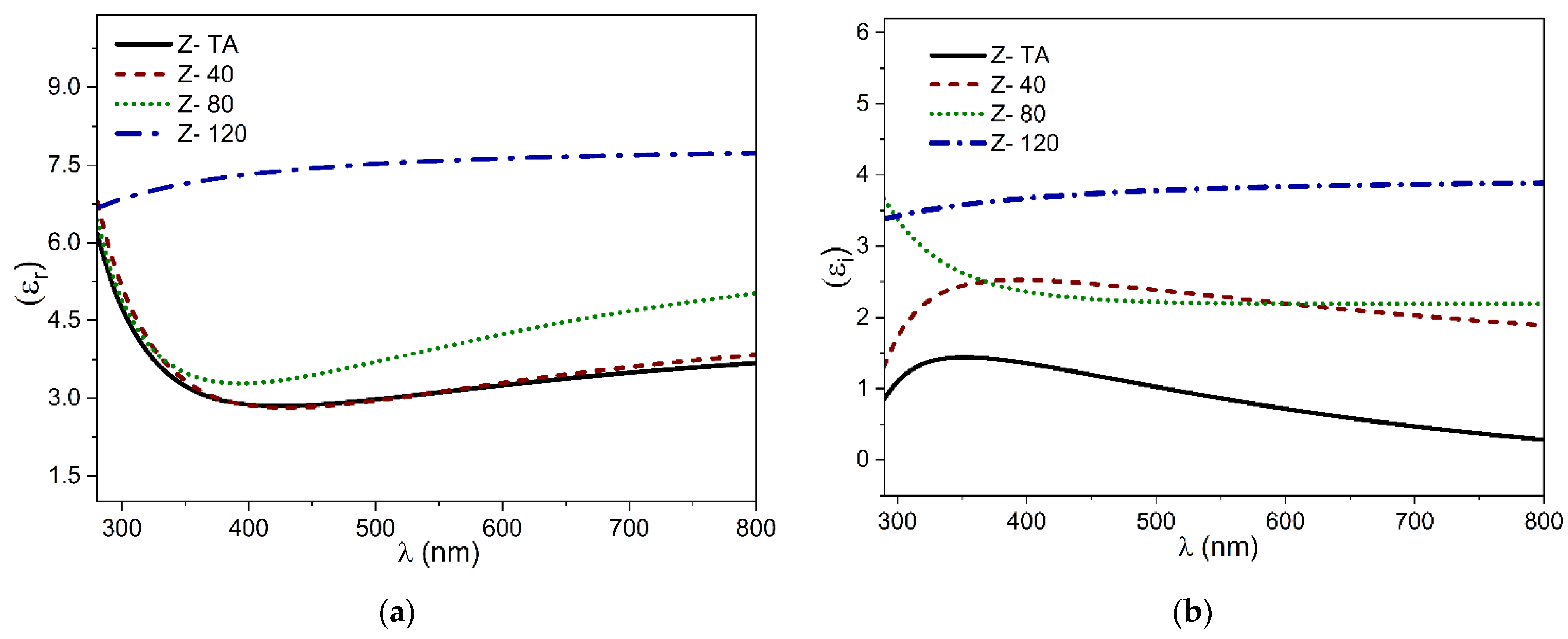
Both components of the dielectric constants (real, εr and imaginary εi) acquired from SE data are plotted in Figure 6a,b. We observed an increase in εr from ~3 (thermally treated ZrO2) to ~7.5 when UV-A treatment is prolonged. The values reported here agrees with the earlier reports [44,45]. Moreover, no critical feature appears in the εi spectra, which again confirms the absence of any crystalline phase present in the films.
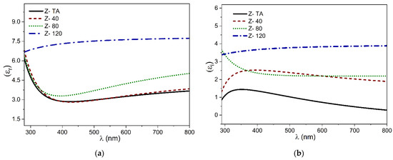
Figure 6.
The dispersion curves of dielectric constants plotted in (a) the real part εr and (b) the imaginary part εi.
3.2.3. Photoluminescence (PL) Studies
The PL technique can investigate into crystalline phases as well as disorder/defects/ impurities of materials and thus help in optimizing the materials’ qualities required for several applications. The emissions observed in PL spectra mostly consist of UV emission, also called near band edge emission (NBE), and visible emission which arise from defects in mediated energy levels. It is now known that the PL spectrum obtained from ZrO2 [46] translates into emissions from defects known as F (anion vacancies) centers and F+ centers as well as from excitons. These defects are mainly controlled by crystalline structure and changes associated with surface morphology [47,48,49]. One should also bear in mind that solution processing [34] is known to create vacancies and interstitials, of both oxygen and Zr in ZrO2 thin films, in quite large numbers and such defects, by introducing new energy levels in the band gap of ZrO2, contribute to emissions too.
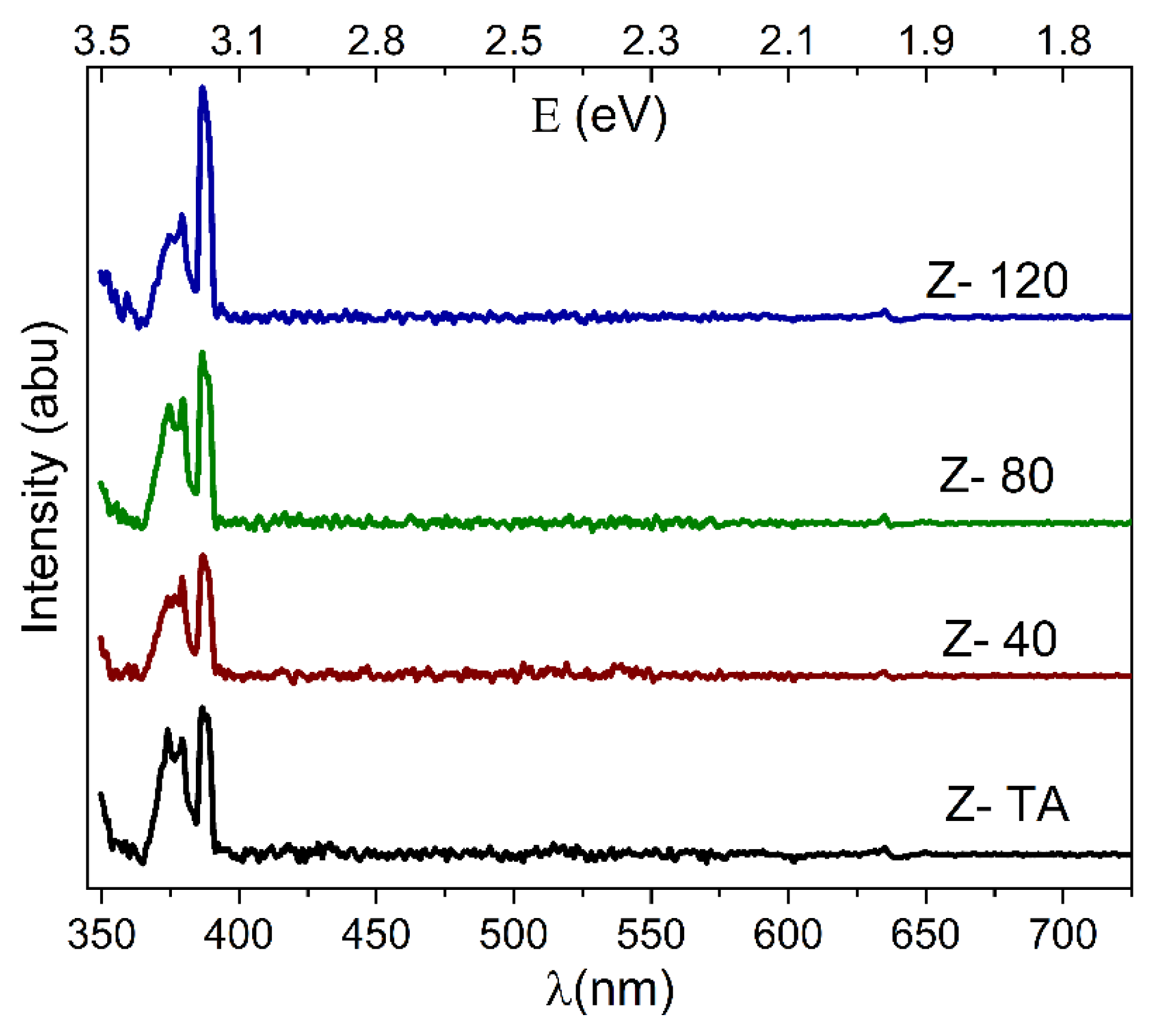
The room temperature PL spectra obtained for thermally treated and UV-A treated ZrO2 thin films are shown in Figure 7. The spectra were background subtracted and de-convoluted with Lorentz distribution function. The positions and full width at half maximum (FWHM) of these de-convoluted peaks/emissions are listed in Table 2. The changes observed in terms of intensity and peak positions clearly demonstrate that UV-A treatment has influenced the luminescence of ZrO2 thin films.
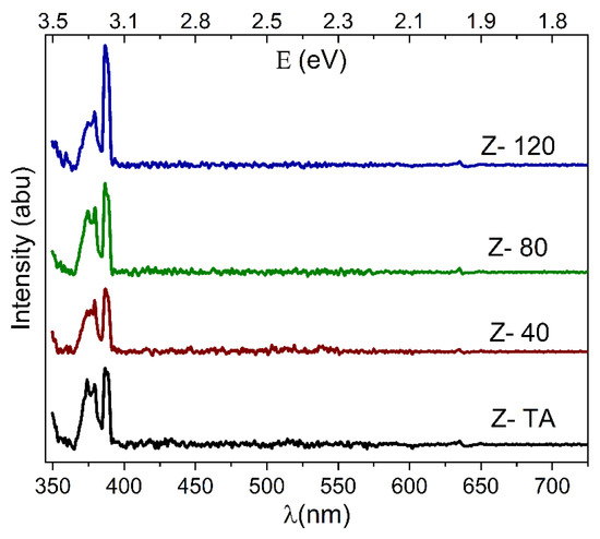
Figure 7.
The PL spectra obtained for thermally treated and UV-A treated ZrO2 films indicate good quality films due to pronounced UV emissions in comparison to visible emissions.
Table 2.
Peaks positions and their FWHM obtained from PL spectra for thermally treated and UV-A treated ZrO2 films.
It is clear from Figure 7, that all the spectra produced distinct emissions in the UV region only and absolutely no emissions in the visible region. These emissions occur at 373 nm (3.32 eV), 379 nm (3.27 eV), 386 nm (3.21 eV), and one at 388 nm (3.19 eV), as shown in Table 2. These emissions are generally recognized as gap states due to the oxygen vacancies [50] in ZrO2 and are produced as a result of radiative recombination of a hole with electron residing in these states. The emissions observed here are in agreement with 379 nm and 390 nm emissions obtained for ZrO2 films fabricated by sol-gel dip coating method [51]. It is important to mention that in oxide based materials, defects and vacancies create defect states near the conduction band edge which can trap the carrier and hence destroy the emissions that result from the band edges [52]. The pronounced UV emissions, as compared to the visible emissions in this study, clearly manifest that the films produced have minimal defects present that can act as trapping centers and hence exhibit great structural quality [53]. Therefore, the water-based solution processing adopted in this study has the potential to produce high-quality ZrO2 thin films which are suitable for applications requiring strong UV emissions.
The effect of UV-A treatment is also quite clear from the Figure 7, which shows that compared to thermally treated ZrO2 film, the UV emission of UV-A exposed films not only grew in intensity but the corresponding FWHM, shown in Table 2, changed as well. UV-A treatment changed the surface morphology, as shown in AFM images, and grains play an important role in controlling the PL intensity [54]. Therefore, it can be speculated that UV-A treatment has helped activate radiative recombination centers (in the grain boundaries) thereby leading to enhanced PL intensity [55]. Moreover, it can also be observed that the PL emissions from UV-A exposed ZrO2 thin films show a minimal shift in their positions, when compared with thermally treated film (see Table 2). This shift, if it occurs, is supposed to be a result of recombination from trapped electrons in the gap states that may result from the formation of Zr = O bond due to bond breaking at the surface [56]. The insignificant shift in PL positions show that UV-A treatment did not cause any restructuring through bond breaking at the surface.
4. Conclusions
The introduction of an environmentally friendlier water-based solution processing, eluding sol-gel procedural complexities altogether, is found as a success to produce ZrO2 films. Further, we have demonstrated successful incorporation of post deposition UV-A = 330 nm treatment in an attempt to lower the deposition temperature of these films.
We showed by XRD and Raman measurements the benefits of increasing UV-A treatment time (0–120 min) in terms of change in structure were similar to thermally treated film as the films maintained their amorphous nature. Change in crystallinity is anticipated for more prolonged exposure, as indicated by the improvement in the only Raman mode observed which is characteristic of the monoclinic phase of ZrO2. In addition, the evolution of surface morphology obtained from AFM studies with regards to the UV-A treatment indicated smooth film surfaces and reduction in surface roughness. The band gap improved (4.54 eV to 4.70 eV) and no tail states were observed in the absorption spectra. The ZrO2 films with UV-A exposure, in comparison to thermal treatment, exhibited a decrease in optical transmittances (94%–88%) while an increase in the refractive index (1.73 to 2.74 measured at 470 nm), leading to less porous films. Low values of extinction coefficient with increasing UV-A exposure confirmed low optical losses in the films. No emissions were observed in the visible region in PL spectra and this together with UV emissions growing in intensity with UV-A treatment indicated high-quality films of ZrO2. This showed that UV-A treatment can be a source to minimize the presence of defects in ZrO2 films. The optical spectroscopy results clearly demonstrated that increased dose of radiation improved the quality of films compared to heat treated films. Furthermore, the study confirmed that the use of UV irradiation has the potential to be an alternative to high temperature annealing process. Although it produces less structural changes in the film when compared with the film treated thermally, it still improves the optical properties due to the change induced in surface morphology by UV-A exposure and high-quality ZrO2 films can be fabricated by a simple, low cost, and environmentally friendlier method with quite an ease without cumbersome sol-gel route.
Author Contributions
Conceptualization, A.B.; investigation, A.B.; methodology and data acquisition, M.F.; formal analysis A.B.; writing—review and editing, A.B.; resources, A.M., S.N. and A.S.B. All authors have read and agreed to the published version of the manuscript.
Funding
This research received no external funding.
Institutional Review Board Statement
Not applicable.
Informed Consent Statement
Not applicable.
Data Availability Statement
Not applicable.
Conflicts of Interest
The authors declare no conflict of interest.
References
- Balog, M.; Schieber, M.; Michman, M.; Patai, S. The chemical vapour deposition and characterization of ZrO2 films from organometallic compounds. Thin Solid Films 1977, 47, 109–120. [Google Scholar] [CrossRef]
- Ibrahim, M.M. Photocatalytic activity of nanostructured ZnO–ZrO2 binary oxide using fluorometric method. Spectrochim. Acta A Mol. Biomol. Spectrosc. 2015, 145, 487–492. [Google Scholar] [CrossRef]
- Zegtouf, H.; Saoula, N.; Azibi, M.; Bait, L.; Madaoui, N.; Khelladi, M.R.; Kechouane, M. A study of properties of ZrO2 thin films deposited by magnetron sputtering under different plasma parameters: Biomedical application. J. Electr. Eng. 2019, 70, 117. [Google Scholar] [CrossRef] [Green Version]
- Khan, M.A.; Gondal, M.A.; Khawaja, E.E. A gas pressure sensor based on ZrO2 thin films for use at high temperatures. Int. J. Electron. 2000, 87, 227–234. [Google Scholar] [CrossRef]
- Velumani, M.; Meher, S.R.; Balakrishnan, L.; Sivacoumar, R.; Alex, Z.C. ZrO2-ZnO composite thin films for humidity sensing. In Proceedings of the AIP Conference, Uttar Pradesh, India, 21–25 December 2016; p. 080032. [Google Scholar]
- Stefanov, P.; Atanasova, G.; Marinova, T.; Gómez-García, J.; Sanz, J.M.; Caballero, A.; Morales, J.J.; Cordón, A.M.; González-Elipe, A.R. Characterization of Co/ZrO2 de-NOX Thin Film Catalysts Prepared by Magnetron Sputtering. Catal. Lett. 2003, 90, 195–203. [Google Scholar] [CrossRef]
- Liu, G.X.; Liu, A.; Shan, F.K.; Meng, Y.; Shin, B.C.; Fortunato, E.; Martins, R. High-performance fully amorphous bilayer metal-oxide thin film transistors using ultra-thin solution-processed ZrOx dielectric. Appl. Phys. Lett. 2014, 105, 113509. [Google Scholar] [CrossRef]
- Oluwabi, A.T.; Katerski, A.; Carlos, E.; Branquinho, R.; Mere, A.; Krunks, M.; Fortunato, E.; Pereira, L.; Oja Acik, I. Application of ultrasonic sprayed zirconium oxide dielectric in zinc tin oxide-based thin film transistor. J. Mater. Chem. C 2020, 8, 3730–3739. [Google Scholar] [CrossRef]
- Pešić, M.; Knebel, S.; Geyer, M.; Schmelzer, S.; Böttger, U.; Kolomiiets, N.; Afanas’ev, V.V.; Cho, K.; Jung, C.; Chang, J.; et al. Low leakage ZrO2 based capacitors for sub 20 nm dynamic random access memory technology nodes. J. App. Phys. 2016, 119, 064101. [Google Scholar] [CrossRef] [Green Version]
- Desforges, J.; Robichaud, L.; Gauvin, S. Determination of Optical Properties of Thin Films from Ketteler-Helmholtz Dispersion Relations: Application to the Case of Ultraviolet Irradiated Zirconium Oxide. Adv. Mater. Sci. Eng. 2017, 2017, 8285230. [Google Scholar] [CrossRef] [Green Version]
- Dong, X.; Xia, G.; Zhang, Q.; Li, L.; Gong, H.; Bi, J.; Wang, S. Room-temperature UV-ozone assisted solution process for zirconium oxide films with high dielectric properties. Ceram. Int. 2017, 43, 15205–15213. [Google Scholar] [CrossRef]
- Méndez-López, A.; Zelaya-Ángel, O.; Toledano-Ayala, M.; Torres-Pacheco, I.; Pérez-Robles, J.F.; Acosta-Silva, Y.J. The Influence of Annealing Temperature on the Structural and Optical Properties of ZrO2 Thin Films and How Affects the Hydrophilicity. Cryst 2020, 10, 454. [Google Scholar] [CrossRef]
- Nishizawa, K.; Miki, T.; Suzuki, K.; Kato, K. Wavelength dependence of crystallization of alkoxy-derived ZrO2 thin films prepared by ultraviolet irradiation. J. Mater. Res. 2005, 20, 3133–3140. [Google Scholar] [CrossRef]
- Heuer, A.H. Science and Technology of Zirconia (Advances in Ceramics); The American Ceramic Society: Westerville, OH, USA, 1981. [Google Scholar]
- Xu, X.; Cui, Q.; Jin, Y.; Guo, X. Low-voltage zinc oxide thin-film transistors with solution-processed channel and dielectric layers below 150 °C. Appl. Phys. Lett. 2012, 101, 222114. [Google Scholar] [CrossRef]
- Azorín, J.; Rivera, T.; Furetta, C.; Sánchez-Rodríguez, A. Ultraviolet Induced Thermoluminescence in Gadolinium-Doped Zirconium Oxide Films. Mater. Sci. Forum. 2005, 480–481, 145–148. [Google Scholar] [CrossRef]
- Han, A.; Ding, H.; Tsoi, J.K.H.; Imazato, S.; Matinlinna, J.P.; Chen, Z. Prolonged UV-C Irradiation is a Double-Edged Sword on the Zirconia Surface. ACS Omega 2020, 5, 5126–5133. [Google Scholar] [CrossRef] [PubMed] [Green Version]
- Chang, C.-L.; Ramanathan, S. A Theoretical Approach to Investigate Low-Temperature Nanoscale Oxidation of Metals under UV Radiation. J. Electrochem. Soc. 2007, 154, G160. [Google Scholar] [CrossRef]
- Tsuchiya, M.; Ramanathan, S. Effect of photon irradiation on structure of yttria-doped zirconia thin films grown on semiconductor substrates. Appl. Phys. Lett. 2007, 91, 253104. [Google Scholar] [CrossRef]
- Liu, G.X.; Liu, A.; Meng, Y.; Shan, F.K.; Shin, B.C.; Lee, W.J.; Cho, C.R. Annealing Dependence of Solution-Processed Ultra-Thin ZrO x Films for Gate Dielectric Applications. J. Nanosci. Nanotechnol. 2015, 15, 2185–2191. [Google Scholar] [CrossRef] [PubMed]
- Lin, C.; Zhang, C.; Lin, J. Phase Transformation and Photoluminescence Properties of Nanocrystalline ZrO2 Powders Prepared via the Pechini-type Sol−Gel Process. J. Phys. Chem. C 2007, 111, 3300–3307. [Google Scholar] [CrossRef]
- Rim, Y.S.; Lim, H.S.; Kim, H.J. Low-Temperature Metal-Oxide Thin-Film Transistors Formed by Directly Photopatternable and Combustible Solution Synthesis. ACS Appl. Mater. Interfaces 2013, 5, 3565–3571. [Google Scholar] [CrossRef]
- Bashir, A.; Majeed, A.; Naseem, S.; Bhatti, A.S. Investigation of structural and optical parameters of yttrium-doped ZnO thin films prepared via spin coating of simple aqueous solution. Bull. Mater. Sci. 2021, 44, 95. [Google Scholar] [CrossRef]
- Li, Z.; Su, K. The direct reaction between CO2 and phenol catalyzed by bifunctional catalyst ZrO2. J. Mol. Catal. A: Chem. 2007, 277, 180–184. [Google Scholar] [CrossRef]
- Jung, K.T.; Shul, Y.G.; Bell, A.T. The preparation and surface characterization of zirconia polymorphs. Korean. J. Chem. Eng. 2001, 18, 992–999. [Google Scholar] [CrossRef]
- Shen, Y.; Shao, S.; Yu, H.; Fan, Z.; He, H.; Shao, J. Influences of oxygen partial pressure on structure and related properties of ZrO2 thin films prepared by electron beam evaporation deposition. Appl. Surf. Sci. 2007, 254, 552–556. [Google Scholar] [CrossRef]
- Manivasakan, P.; Rajendran, V.; Ranjan Rauta, P.; Bandhu Sahu, B.; Krushna Panda, B. Synthesis of Monoclinic and Cubic ZrO2 Nanoparticles from Zircon. J. Am. Ceram. Soc. 2011, 94, 1410–1420. [Google Scholar] [CrossRef]
- Benyagoub, A.; Levesque, F.; Couvreur, F.; Gibert-Mougel, C.; Dufour, C.; Paumier, E. Evidence of a phase transition induced in zirconia by high energy heavy ions. Appl. Phys. Lett. 2000, 77, 3197–3199. [Google Scholar] [CrossRef]
- Tiseanu, C.; Cojocaru, B.; Parvulescu, V.; Sanchez-Dominguez, M.; Primus, P.-A.; Boutonnet, M. Order and disorder effects in nano-ZrO2 investigated by micro-Raman and spectrally and temporarily resolved photoluminescence. Phys. Chem. Chem. Phys. 2012, 14, 12970–12981. [Google Scholar] [CrossRef]
- Strekalovskii, V.N.; Vovkotrub, É.G. Raman spectroscopy of materials based on zirconium dioxide. Refractories 1985, 26, 151–162. [Google Scholar] [CrossRef]
- Mirgorodsky, A.P.; Smirnov, M.B.; Quintard, P.E. Phonon spectra evolution and soft-mode instabilities of zirconia during the c-t-m transformation. J. Phys. Chem. Solids 1999, 60, 985. [Google Scholar] [CrossRef]
- Branquinho, R.; Salgueiro, D.; Santos, L.; Barquinha, P.; Pereira, L.; Martins, R.; Fortunato, E. Aqueous Combustion Synthesis of Aluminum Oxide Thin Films and Application as Gate Dielectric in GZTO Solution-Based TFTs. ACS Appl. Mater. Interfaces 2014, 6, 19592–19599. [Google Scholar] [CrossRef]
- Zhu, C.; Liu, A.; Liu, G.; Jiang, G.; Meng, Y.; Fortunato, E.; Martins, R.; Shan, F. Low-temperature, nontoxic water-induced high-k zirconium oxide dielectrics for low-voltage, high-performance oxide thin-film transistors. J. Mater. Chem. C 2016, 4, 10715–10721. [Google Scholar] [CrossRef]
- Cong, Y.; Li, B.; Lei, B.; Li, W. Long lasting phosphorescent properties of Ti doped ZrO2. J. Lumin. 2007, 126, 822–826. [Google Scholar] [CrossRef]
- Takahashi, T.; Nakabayashi, H.; Terasawa, T.; Masugata, K. Atomic force microscopy observation of TiO2 films deposited by dc reactive sputtering. J. Vac. Sci. Technol. A 2002, 20, 1205–1209. [Google Scholar] [CrossRef]
- Martin, N.; Rousselot, C.; Rondot, D.; Palmino, F.; Mercier, R. Microstructure modification of amorphous titanium oxide thin films during annealing treatment. Thin Solid Films 1997, 300, 113–121. [Google Scholar] [CrossRef]
- Bensaha, R.; Bensouyad, H. Heat Treatment—Conventional and Novel Applications; Czerwinski, F., Ed.; IntechOpen: London, UK, 2012. [Google Scholar] [CrossRef] [Green Version]
- Joy, K.; Berlin, I.J.; Nair, P.B.; Lakshmi, J.S.; Daniel, G.P.; Thomas, P.V. Effects of annealing temperature on the structural and photoluminescence properties of nanocrystalline ZrO2 thin films prepared by sol–gel route. J. Phys. Chem. Solids 2011, 72, 673–677. [Google Scholar] [CrossRef]
- Liu, M.; Fang, Q.; He, G.; Li, L.; Zhu, L.Q.; Li, G.H.; Zhang, L.D. Effect of post deposition annealing on the optical properties of HfOxNy films. Appl. Phys. Lett. 2006, 88, 192904. [Google Scholar] [CrossRef]
- French, R.H.; Glass, S.J.; Ohuchi, F.S.; Xu, Y.N.; Ching, W.Y. Experimental and theoretical determination of the electronic structure and optical properties of three phases of ZrO2. Phys. Rev. B 1994, 49, 5133–5142. [Google Scholar] [CrossRef]
- Yusoh, R.; Horprathum, M.; Eiamchai, P.; Chindaudom, P.; Aiempanakit, K. Determination of Optical and Physical Properties of ZrO2 Films by Spectroscopic Ellipsometry. Procedia Eng. 2012, 32, 745–751. [Google Scholar] [CrossRef] [Green Version]
- Wang, X.; Wu, G.; Zhou, B.; Shen, J. Effect of crystal structure on optical properties of sol–gel derived zirconia thin films. J. Alloys Compd. 2013, 556, 182–187. [Google Scholar] [CrossRef]
- Dimitrov, O.; Stambolova, I.; Vassilev, S.; Lazarova, K.; Babeva, T.; Mladenova, R. Surface and Morphological Features of ZrO2 Sol-Gel Coatings Obtained by Polymer Modified Solution. Mater. Proc. 2020, 2, 6. [Google Scholar] [CrossRef]
- An I, L.S.; Kang, B.; Lee, S.; Jeong, H.; Song, C. Optical, Electrical, and Structural Properties of Ultrathin Zirconium-oxide Films. J. Korean Phys. Soc. 2010, 57, 1811–1815. [Google Scholar] [CrossRef]
- Li, J.; Meng, S.; Niu, J.; Lu, H. Electronic structures and optical properties of monoclinic ZrO2 studied by first-principles local density approximation + U approach. J. Adv. Ceram. 2017, 6, 43–49. [Google Scholar] [CrossRef] [Green Version]
- Arsenev, P.A.; Bagdasarov, K.S.; Niklas, A.; Ryazantsev, A.D. X-ray and thermostimulated luminescence of 0.9 ZrO2–0.1 Y2O3 Single Crystals. Phys. Status Solidi (A) 1980, 62, 395–398. [Google Scholar] [CrossRef]
- Kumar, S.; Bhunia, S.; Ojha, A.K. Effect of calcination temperature on phase transformation, structural and optical properties of sol–gel derived ZrO2 nanostructures. Phys. E Low-Dimen Syst. Nanostruct. 2015, 66, 74–80. [Google Scholar] [CrossRef]
- Ghosh, M.; Karmakar, D.; Basu, S.; Jha, S.N.; Bhattacharyya, D.; Gadkari, S.C.; Gupta, S.K. Effect of size and aspect ratio on structural parameters and evidence of shape transition in zinc oxide nanostructures. J. Phys. Chem. Solids 2014, 75, 543–549. [Google Scholar] [CrossRef] [Green Version]
- Kumar, S.; Ojha, A.K. Room temperature ferromagnetism in undoped and Mn doped t-ZrO2 nanostructures originated due to oxygen vacancy and effect of Mn doping on its optical properties. Mater. Chem. Phys. 2016, 169, 13–20. [Google Scholar] [CrossRef]
- Emeline, A.; Kataeva, G.V.; Litke, A.S.; Rudakova, A.V.; Ryabchuk, V.K.; Serpone, N. Spectroscopic and Photoluminescence Studies of a Wide Band Gap Insulating Material: Powdered and Colloidal ZrO2 Sols. Langmuir 1998, 14, 5011–5022. [Google Scholar] [CrossRef]
- Lakshmi, J.S.; John Berlin, I.; Daniel, G.P.; Thomas, P.V.; Joy, K. Effect of calcination atmosphere on photoluminescence properties of nanocrystalline ZrO2 thin films prepared by sol–gel dip coating method. Physica B 2011, 406, 3050–3055. [Google Scholar] [CrossRef]
- Rajabi, M.; Shogh, S.; Iraji zad, A. Defect study of TiO2 nanorods grown by a hydrothermal method through photoluminescence spectroscopy. J. Lumin. 2015, 157, 235–242. [Google Scholar] [CrossRef]
- Kumari, L.; Li, W.Z.; Xu, J.M.; Leblanc, R.M.; Wang, D.Z.; Li, Y.; Guo, H.; Zhang, J. Controlled Hydrothermal Synthesis of Zirconium Oxide Nanostructures and Their Optical Properties. Cryst. Growth Des. 2009, 9, 3874–3880. [Google Scholar] [CrossRef]
- Matsumoto, T.; Kato, H.; Miyamoto, K.; Sano, M.; Zhukov, E.A.; Yao, T. Correlation between grain size and optical properties in zinc oxide thin films. Appl. Phys. Lett. 2002, 81, 1231–1233. [Google Scholar] [CrossRef]
- López, M.; Garrido, B.; García, C.; Pellegrino, P.; Pérez-Rodríguez, A.; Morante, J.R.; Bonafos, C.; Carrada, M.; Claverie, A. Elucidation of the surface passivation role on the photoluminescence emission yield of silicon nanocrystals embedded in SiO2. Appl. Phys. Lett. 2002, 80, 1637–1639. [Google Scholar] [CrossRef]
- Wolkin, M.V.; Jorne, J.; Fauchet, P.M.; Allan, G.; Delerue, C. Electronic States and Luminescence in Porous Silicon Quantum Dots: The Role of Oxygen. Phys. Rev. Lett. 1999, 82, 197–200. [Google Scholar] [CrossRef]


Publisher’s Note: MDPI stays neutral with regard to jurisdictional claims in published maps and institutional affiliations. |
© 2021 by the authors. Licensee MDPI, Basel, Switzerland. This article is an open access article distributed under the terms and conditions of the Creative Commons Attribution (CC BY) license (https://creativecommons.org/licenses/by/4.0/).