Article

The Effect of Match between High Power Impulse and Bias Voltage: TiN Coating Deposited by High Power Impulse Magnetron Sputtering

1
Department of Materials Engineering, Ming Chi University of Technology, New Taipei City 24301, Taiwan
2
Center for Plasma and Thin Film Technologies, Ming Chi University of Technology, New Taipei City 24301, Taiwan
3
Bachelor Program in Interdisciplinary Studies, National Yunlin University of Science and Technology, Yunlin County 63201, Taiwan
*
Author to whom correspondence should be addressed.
Coatings 2021, 11(7), 822; https://doi.org/10.3390/coatings11070822
Submission received: 24 June 2021 / Revised: 2 July 2021 / Accepted: 6 July 2021 / Published: 7 July 2021
(This article belongs to the Special Issue Magnetron Sputter Deposition of Nitride Thin Films and Nanostructures)

Abstract

:
Practical experience in the use of high power impulse magnetron sputtering (HiPIMS) technology has revealed that output bias current depends on the total energy output of the cathodes, which means that bias voltage settings do not necessarily match the actual output. In this study, we investigated the effects of bias current and voltage on the characteristics of titanium nitride thin films produced using high impulse magnetron sputtering. The bias current and voltage values were adjusted by varying the supplied cathode power and substrate bias under DC and pulsed-DC output models. Our results revealed that pulse delay (PD) and feed forward (FF) settings can be used to control bias current and voltage. Increasing the bias current from 0.56 to 0.84 was shown to alter the preferred orientation from (111) to (220), increase the deposition rate, and lead to a corresponding increase in film thickness. The surface morphology of all titanium nitride samples exhibited tapered planes attributable to the low bias current and voltage (−30 V). The maximum hardness values were as follows: DC mode (23 GPa) and pulsed-DC mode (19 GPa). The lower hardness values of pulsed-DC samples can be attributed to residual stress, preferred orientation, and surface morphology. The surface of the samples was shown to be hydrophobic, with contact angles of >100°.

1. Introduction

Titanium nitride (TiN) is a protective coating widely used in cutting tools and mechanical components in the aerospace industry, due to its high hardness and excellent wear and corrosion resistance [1,2,3]. TiN films are also used as diffusion barriers for Al-based interconnects [4], as well as many decorative applications [5,6]. Numerous methods have been developed for the deposition of TiN coatings, including cathode vacuum arc evaporation (CVAE) [7], DC and pulsed-DC magnetron sputtering (DCMS, P-DCMS) [8,9], and high-power impulse magnetron sputtering (HiPIMS) [10]. The high processing temperatures and corresponding high ionization rates associated with CVAE often lead to melting of the target surface, resulting in micrometre-sized particles in the arc discharge region. This has limited CVAE to specific applications that permit high-temperature processing and do not require smooth surfaces [11]. The low processing temperature and corresponding low rate of ionization associated with DCMS produces smooth coating surfaces; however, the density of the resulting films tends to be quite low. HiPIMS has proven superior to conventional methods based on physical vapour deposition in terms of film density, hardness, and surface smoothness [12]. The high ionized flux fraction, instantaneous current delivery, high peak power density, and high plasma density of HiPIMS allows for a low duty cycle (<5%) and low frequency operation (<1 kHz) with short pulse-on times and long pulse-off times [13]. Paulitsch et al. [14] reported that TiN and CrN coatings deposited using DCMS present a columnar grain morphology, whereas the coatings deposited using HiPIMS provide higher density, superior uniformity, and higher hardness. Elmkhah et al. [15] reported that changing the supplied power from DC to HiPIMS altered the preferred orientation of TiN films from (111) to (200). Magnus et al. [16] reported that the resistivity of films deposited using HiPIMS is far lower than that of DCMS films, particularly at low temperatures. They attributed this difference to reduced scattering at grain boundaries.
The basic structure of a HiPIMS power supply is as follows: 1. A DC generator charges the bank of capacitors C in a pulsing unit; 2. Energy stored in the capacitors is then dissipated into plasma by fast-switching pulses with a clearly defined width and frequency [17]. HiPIMS power supplies with large capacitors tend to produce pulses of high currents, which is amenable to the deposition of high-density films with low surface roughness [17]. In the event that the current exceeds a critical value, the output of the power supply is instantaneously cut off. This protection mechanism is meant to protect the power supply from damage due to a high current. A similar protection mechanism is also used to safeguard the substrate voltage system. Note, however, that the instantaneous delivery of a high current and voltage at the instant arcing occurs can trigger the power supply to switch off, which increases the degree of uncertainty in the deposition process.
Substrate bias voltage is a key parameter in the film deposition process, due to the fact that bombardment by high-energy ions can enhance atom migration, promote the desorption of physically adsorbed atoms and shallow ion implantation, and capture impacting atoms [18]. Applying negative bias voltage to a substrate has been shown to alter the film properties significantly in terms of grain size, deposition rate, hardness, and residual stress. Bhaduri et al. [19] reported that increasing the bias voltage resulted in a smaller grain size. Guruvenket et al. [20] reported that increasing the bias voltage from 0 to −40 V led to a corresponding increase in residual stress from +5 to −25 GPa. Note, however, that increasing the bias voltage further did not have a significant effect on residual stress. The application of pulsed-DC (P-DC) bias during deposition has been shown to reduce the deposition temperature and maintain a higher net deposition rate, compared to conventional DC bias voltage. Cooke et al. [21] and Olbrich et al. [22] reported that P-DC eliminates the risk of arcing, allows for the ionic cleaning of insulating oxide films and oxide surfaces without causing problems related to substrate charging, permits lower operating voltages, and improves coating adhesion at low temperatures.
During the film deposition process, high currents and voltage are generated at the instant arcing occurs, causing the DC-bias output of the substrate to be interrupted via the above-mentioned protection mechanism. Under these circumstances, the deposition rate is low, and the adhesion of the resulting film is poor.
In this work, TiN films were deposited using a HiPIMS with various control modes implemented via power supply settings. Two HiPIMS power supplies and one bias voltage (DC or pulsed-DC) were used to deposit TiN thin films. Pulse delay (PD) was used to alternate the power delivery to the two targets in order to prevent bias voltage failure (switch off) caused by excessive current output. Feed Forward (FF) control was used to make the HiPIMS output time responsive to bias voltage in order to prevent excessively high currents from causing bias voltage failure. Samples were created using eight combinations of PD and FF under DC or P-DC bias output modes in order to elucidate the effects of bias current and voltage on the microstructural and mechanical characteristics of TiN thin films.

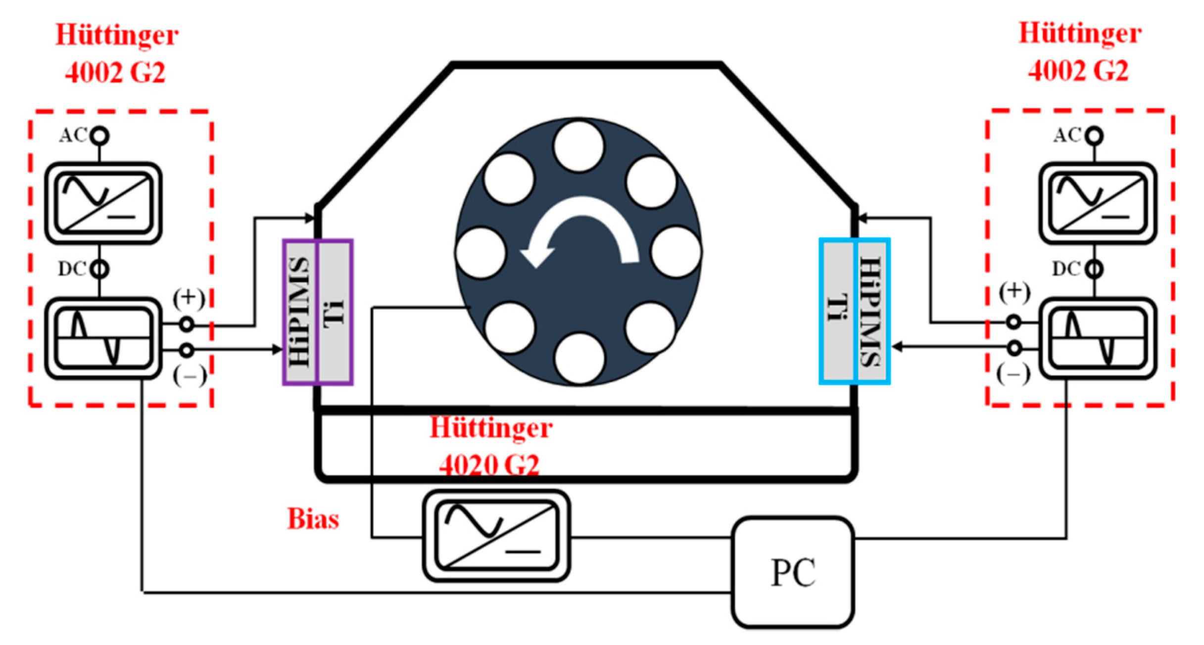
2. Experiment Details

HiPIMS was used to fabricate TiN coatings on P-type (100) Si and high-speed steel (HSS: SKH9; radius = 14.5 mm; thickness = 8 mm) substrates using dual Ti targets under an N2/Ar gas environment. A schematic diagram of the experiment apparatus is presented in Figure 1. A titanium target (purity of 99.99%) covering 542.5 cm2 was connected to a pulsed power supply in unipolar output mode. During the deposition process, the temperature in the chamber increased from room temperature to 60 °C without supplemental heating. The samples (HSS and Si substrates) underwent ultrasonic cleaning with acetone and ethanol solution for 15 min, followed by drying under pure nitrogen, before being fixed on a substrate holder in the vacuum chamber to enable rotation at 3 rpm. The base pressure prior to the experiment was 2 × 10⁻⁵ Pa. Plasma etching was conducted via Ar glow discharge with a DC bias of −800 V under a pressure of 0.5 Pa. Metal ion bombardment was then conducted via HiPIMS with a gradual reduction in DC bias from −800 to −600 V, and then to −400 and −200 V in intervals of 5 min. The Ar flow rate was maintained at 90 sccm and the bias voltage was reduced to −45 V during subsequent processing. The power applied to the Ti targets was 2.5 kW. A Ti adhesion layer was deposited on the substrate via HiPIMS under the Ar environment. The deposition duration of the TiN working layer was 180 min under a working pressure of 0.4 Pa (N2/Ar flow ratio: 9%). The deposition parameters are detailed in Table 1. We employed two HiPIMS power supplies and a single bias power supply (operable in DC or pulsed-DC mode) for the deposition of the TiN coatings. As shown in Table 2, two categories of samples were created: DC bias (DC) and pulsed-DC bias (P-DC) mode. These categories were subdivided into four combinations of PD and FF as follows: H, H-PD, H-FF, and H-PD-FF. The peak power density ranged from 448 to 455 W/cm2 regardless of operating mode (see Table 2).
A digital oscilloscope (GW Instek GDS-2204E, New Taipei City, Taiwan) was used with a differential voltage probe (GDP-025) and an active current probe (GCP-020) to record the voltage and current. The surface morphologies of the coatings on Si wafer were characterized by field emission scanning electron microscopy (FE-SEM, JEOL, JSM-7610F, Tokyo, Japan). The crystal structure and preferred orientation of the formed coatings was characterized by glancing angle X-ray diffraction (GIXRD, PANalytical, X’pert, Almelo, The Netherlands) with monochromatic Cu Kα radiation. The diffraction patterns were obtained between 20° and 90°. The preferred orientation in the coating was determined by calculating the texture coefficient Tc (hkl) for each orientation using:
Tc h k l = I h k l / I o h k l 1 n 1 n I h k l / I o h k l
where I(hkl) is the diffraction peak of the measured sample from the (hkl) plane, Io(hkl) is the diffraction peak of the standard reference (JCPDS database) in same plane, and n indicates the total number of diffraction peaks from the coating. The chemical composition of the coatings was determined employing wavelength dispersive electron-probe micro-analysis (EPMA, JEOL, JXA-8500F, Tokyo, Japan). The coatings on the HSS substrates were analyzed for mechanical properties. The residual stress of the coatings was evaluated using the substrate curvature method (FSMI, PSC-2320-S, PENTAD, New Taipei city, Taiwan), which involved measuring the thickness of the coatings and the curvature of the Si wafer before and after deposition. Residual stress was calculated using Stoney’s equation [23]. The mechanical properties of the coatings (hardness and Young’s modulus) were determined by nanoindentation. A commercially available nanoindenter (TI-900, Triboin-denter, Hysitron Inc., Minneapolis, MN, USA) was used for the nanoindentation test. Under a peak load of 0.5–10 mN, a Berkovich diamond indenter with a nominal tip radius of 100 nm was used for indentation. In order to minimize the influence of the substrate on the hardness measurement, the maximum indentation depth should be limited to less than one-tenth of the coating thickness. Eight results were recorded to capture the average values of hardness and elastic modulus.

3. Results and Discussion

Figure 2 presents waveforms showing the target voltage (Vt), target current (It), bias voltage (Vb), and bias current (Ib) during reactive HiPIMS of Ti under an N2/Ar environment (no specific operating mode). The Vt and It values indicate that the output time interval of target A and B changed seemingly at random. The time interval of targets A and B were 2200 or 5000 μs, due to the fact that the start time of HiPIMS power was not fixed and the power supplies were subject to re-starting when arcing occurred. Note the results in Figure 2 were recorded under the same batch at different times. The sharp Vb and Ib peaks corresponded to Vt and It associated with charged ions in the plasma arriving at the substrate surface. In order to eliminate the problem of two power supplies, the cathode cannot be synchronized. Software was used to synchronize the operations of the two HiPIMS power supplies, i.e., establish set intervals between the operations of targets A and B. Figure 3 presents the Vt, It, Vb, and Ib waveforms under the PD mode. The interval between the operations of targets A and B was fixed at 2500 μs. The sharp Vb and Ib waveforms corresponded to the Vt and It values mentioned previously (charged ions in the plasma). As shown in Table 3, the interval between the operations of targets A and B does not depend on whether the system is operating in DC or P-DC mode. It means that the interval between the operations of targets A and B must be effectively controlled through software. When the HiPIMS power and bias mode was changed from unspecified to merge mode under DC bias, the value of Ib increased from 0.56 to 0.67 A, and the value of Vb increased from −30.8 to −32.6 V. When the HiPIMS power and bias mode was changed from unspecified to merge mode under P-DC bias, the value of Ib increased from 0.71 to 0.84 A, and the value of Vb increased from −32.8 to −34.9 V. This can be attributed to a decrease in the number of times the HiPIMS power supply had to be restarted in response to arcing events. We can use this information when establishing fixed time intervals for targets A and B via signal transmission from the HiPIMS power supply to the substrate bias power supply.
EPMA measurements revealed that the atomic percentage remained constant: Ti (45.5 at.%), N (50.5 at.%), and O (3–4 at.%). The N/Ti ratio was maintained at a constant ~1.09 to 1.12, indicating TiN coating in stoichiometric quantities [24]. Figure 4 presents the deposition rate and final thickness of TiN, and the corresponding Ib values as a function of the HiPIMS operating mode under DC or P-DC bias. An increase in Ib (from 0.56 to 0.84 A) was associated with an increase in the deposition rate (from 6.88 to 8.08 nm/min) and a corresponding increase in the final thickness of the TiN layer (from 1.65 to 1.94 µm). This correlation between Ib value and film thickness can be attributed to an increase in the deposition of ionized particles on the surface of the substrate under the effects of enhanced ion bombardment due to highly ionized plasma [25,26].
Figure 5 presents XRD patterns of TiN coatings deposited using various HiPIMS operating modes under DC or P-DC bias. The diffraction peaks at 2θ = 36.7°, 42.6°, 61.8°, and 74.2° correspond to the (111), (200), (220), and (311) planes in an NaCl-type face centered cubic (FCC) structure of TiN, in accordance with JCPDS No. 3-65-0970. The texture coefficient was used to estimate changes in the preferred orientation in samples created under DC or P-DC bias. Note that under DC bias, the preferred orientation was (111), whereas under P-DC bias, the preferred orientation was (220). Note that a few previous studies described the (220) preferred orientation in TiN coatings [4,19,27]. The preferred orientation depends on a variety of processing conditions, including substrate temperature, bias voltage, cathode power, deposition pressure, and bombardment energy. Figure 6 presents the texture coefficient and Ib of all samples obtained using all of the deposition parameter sets. Under DC bias, an increase in Ib (from 0.56 to 0.67 A) was correlated with a notable decrease in the (111) texture coefficient and a corresponding increase in the (220) texture coefficient. Under P-DC bias, an increase in Ib (from 0.71 to 0.84 A) had the same effect on the (111) and (220) texture coefficients. These findings are in line with those reported by Hurkmans et al. [28] and Lee et al. [29], who described a shift in the preferred orientation from (111) to (220) with an increase in bias current. Park et al. [30] also reported that under a fixed substrate bias, an increase in substrate current density (associated with an increase in ion bombardment) produced a shift in the preferred orientation from TiN (200) to TiN (220).
Figure 7 presents top-view SEM images of TiN coatings created using various HiPIMS operating modes under DC or P-DC bias. All of the coatings presented a columnar surface structure with trigonal-shaped facets, which is an indirect indication of the (111) preferred orientation seen in the XRD results [30]. The surface morphology of TiN can be attributed to low bias voltage (−30 V) and substrate bias current. The surface morphology created under P-DC output presented a larger proportion of pyramidal grains than was observed in samples created under DC mode. This can be attributed to a shift in the preferred orientation from (111) to (220) when the bias voltage was changed from DC to P-DC output mode. Cheng et al. [31] and Li et al. [25] reported that film with a (110) texture presents a star-shaped topography, whereas film with a (111) texture presents a trigonal-shaped topography. Note that the samples created using pulsed-DC bias voltage presented smaller grains with a larger proportion of trigonal-shaped facets. The surface roughness (Ra) values of the various TiN films created under DC mode were follows: 29 nm (H), 30 nm (H-PD), 25 nm (H-FF), and 25 nm (H-PD-FF). The surface roughness (Ra) values of the various TiN films created under P-DC mode were follows: 26 nm (H), 24 nm (H-PD), 19 nm (H-FF), and 20 nm (H-PD-FF). Overall, the surface roughness values of films created in DC mode were far higher than those created in P-DC mode.
As shown in Table 4, under DC bias, the hardness values ranged from 22.7 ± 1.1 to 23.2 ± 0.7 GPa, and the Young’s modulus ranged from 367 ± 9.6 to 385 ± 14.5 GPa. Under P-DC bias, the hardness values ranged from 18.5 ± 0.7 to 19.3 ± 0.7 GPa, and the Young’s modulus ranged from 315 ± 9.4 to 327 ± 6.5 GPa. The difference in hardness can be attributed to texture, residual stress, and surface morphology. Ljungcrantz et al. [32] reported that hardness values can be characterized in terms of texture, as follows: (111) > (100) > (220). Chang et al. [33] reported that hardness values are proportional to residual stress. In the current study, the TiN coatings created under DC bias presented a high (111) texture coefficient and high residual stress, which resulted in hardness of 23.2 ± 0.7 GPa, regardless of the operating mode (see Table 4). The lower hardness values under P-DC bias can be attributed to the film surface presenting tetrahedral and pyramidal structures set at wide intervals, resulting in relatively low film density. Wang et al. [34] reported that increasing the bias voltage from −50 to −300 V led to a corresponding increase in TiN hardness from 4.66 ± 0.18 to 17.4 ± 0.53 GPa, attributable to an increase in structural density and a decrease in crystallite size. In this study, the bias voltage was fixed at −30 V. When the bias mode was changed from DC to P-DC mode, the value of Vb increased from −30.8 to −34.9 V. However, the value of hardness and residual stress are inversely proportional to Vb. This can be attributed to the variation of Vb is smaller than texture coefficient. Although the PD and FF settings were added, the value of hardness did not increase significantly, which effectively reduced the residual stress.
The lower hardness values in the current study can be attributed to the texture. Nonetheless, the (220) preferred orientation in our TiN coatings could be used for a hard ceramic protective coating to improve the hydrophobia of bipolar plates used in Proton Exchange Membrane Fuel Cell (PEMFC) [35]. Note also that the trigonal-shaped facets increased the water contact angle. Figure 8 shows the contact angles of deionized water on TiN coatings created using various HiPIMS operating modes under DC or P-DC bias. The contact angles of the TiN coatings created under DC bias mode were as follows: unspecified (106.7°), PD (113.7°), FF (102.4°), and merge mode (109.5°). The contact angles of the TiN coatings created under P-DC bias mode were as follows: unspecified (103.6°), PD (113.3°), FF (105.3°), and merge mode (116.5°). Generally, a surface is considered hydrophilic if the contact angle is <90°, whereas it is considered hydrophobic if the contact angle is >90° [36]. All of the samples in the current study were hydrophobic.

4. Conclusions

Our primary objective in this study was to elucidate the effects of substrate current on the properties of TiN layers created using various HiPIMS operating modes under DC or P-DC bias. The conclusions are outlined in the following:
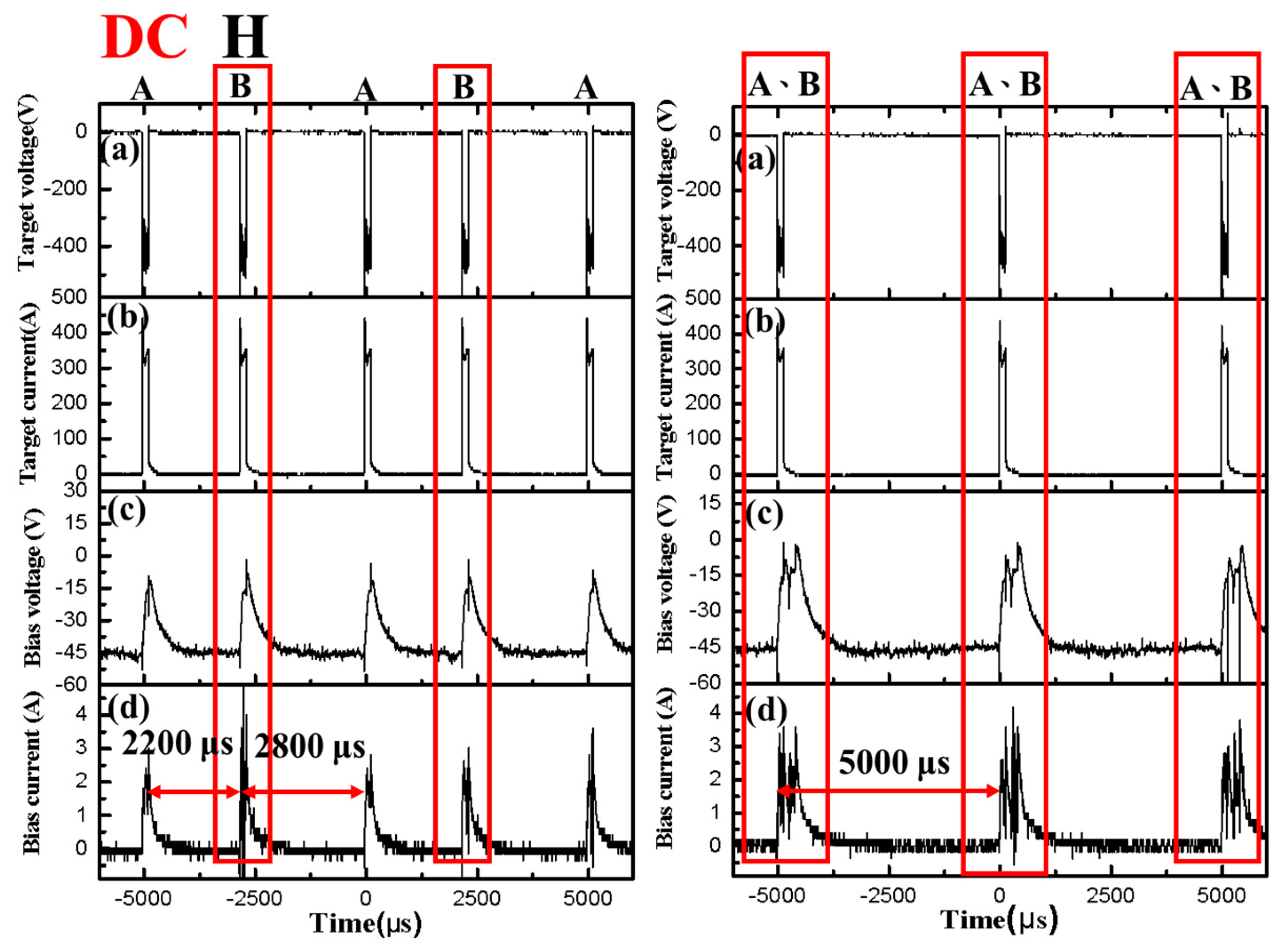
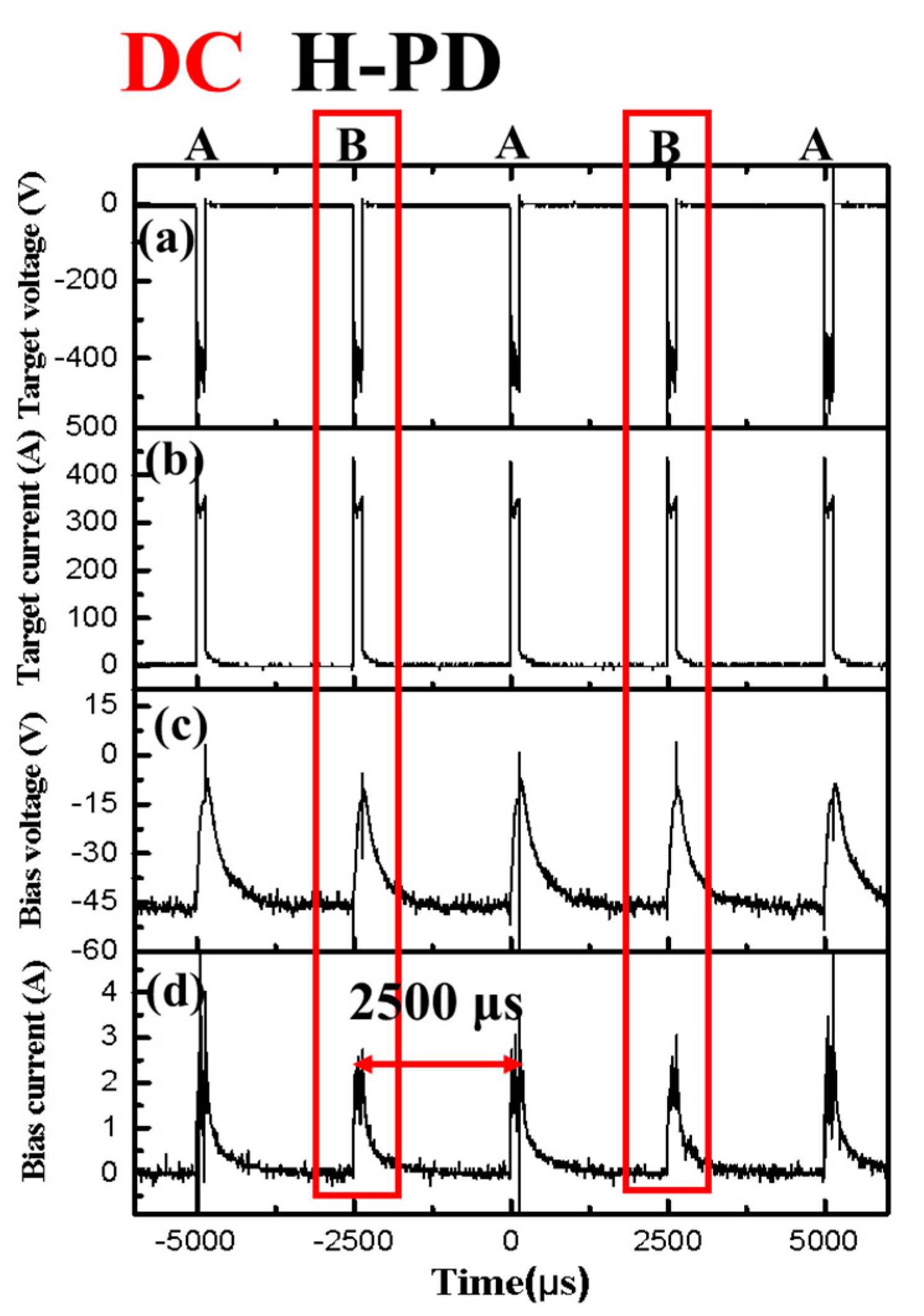
  • The Ib waveforms revealed that the output interval affected the Ib value. The Ib increased when the time interval was changed from random to regular (DC or pulsed-DC). Furthermore, FF setting can be used to reduce Vb.
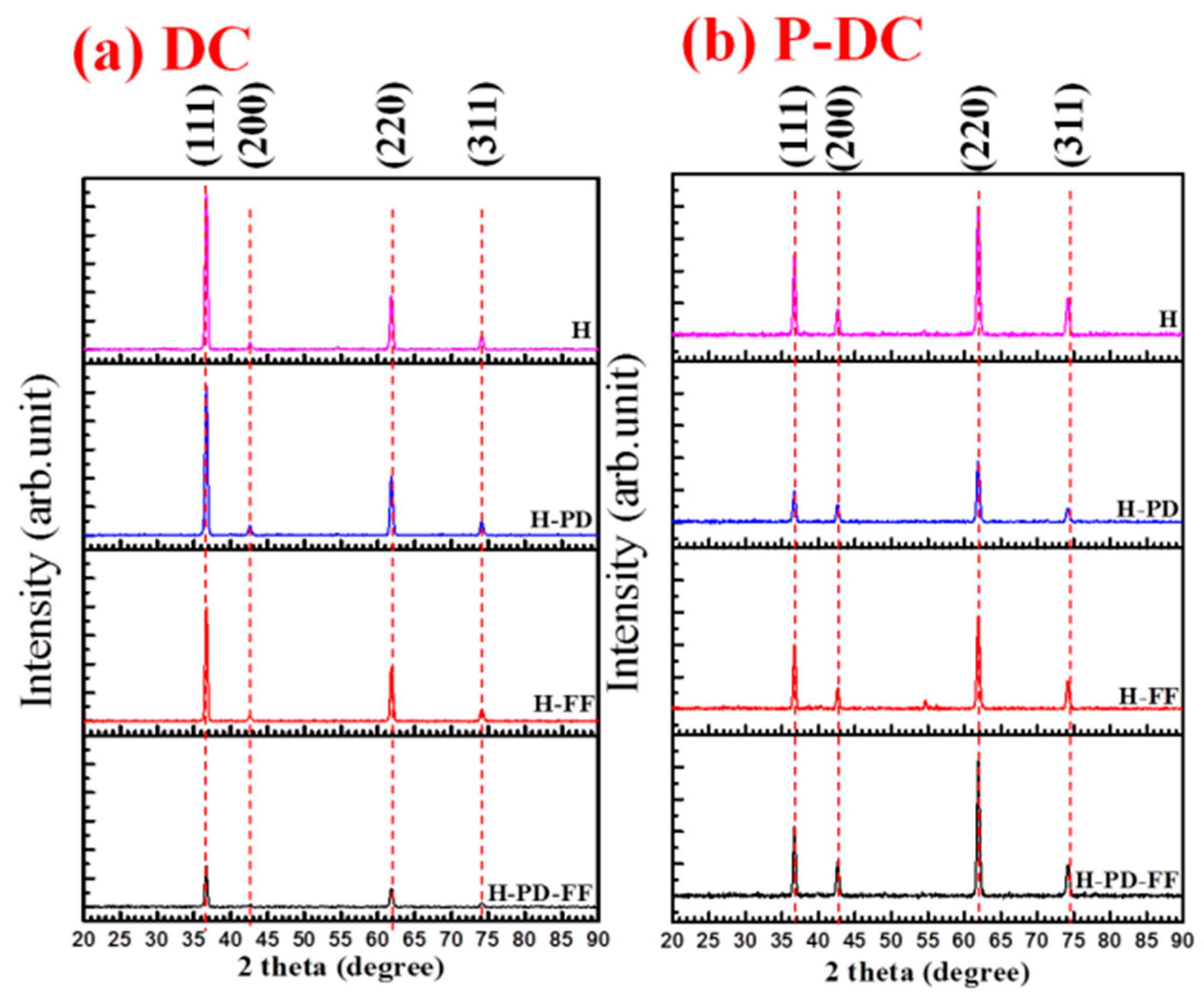
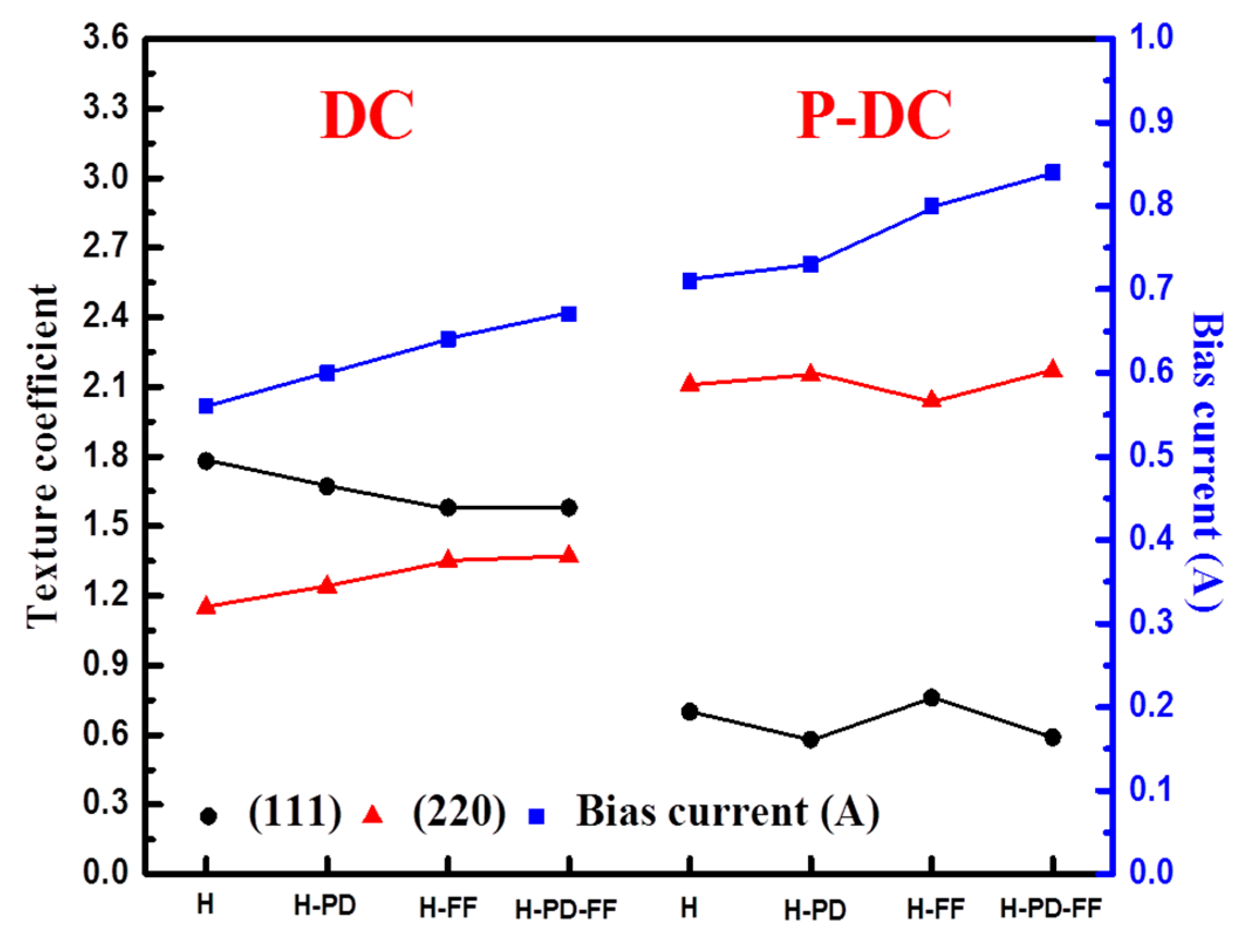
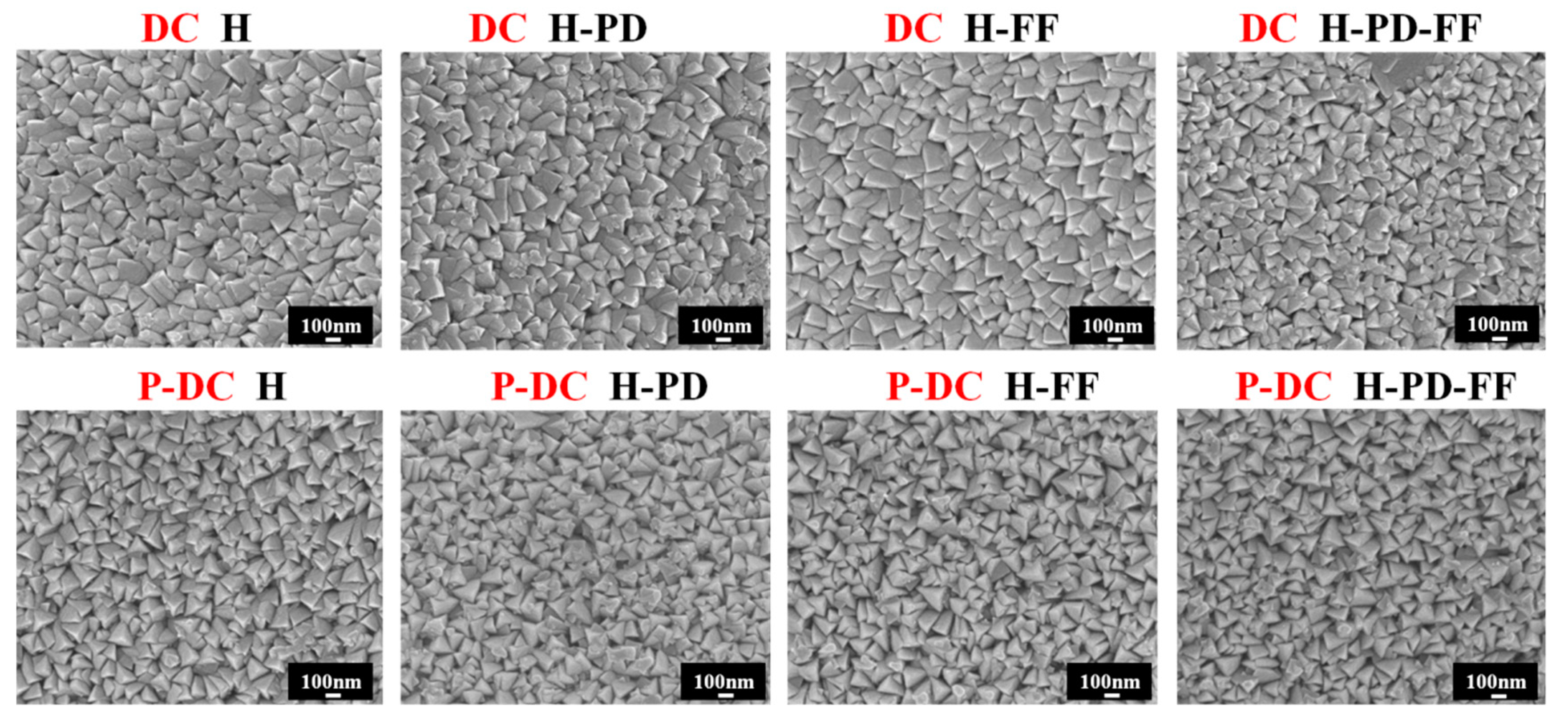
  • XRD analysis revealed that TiN exhibited a strong (111) preferred orientation under DC mode and a strong (220) preferred orientation under pulsed-DC mode. This can be attributed to higher substrate current and ion bombardment energy, which also increased the deposition rate and final thickness of TiN.
  • The highest hardness values achieved in the current study (23.2 GPa) were obtained in PD and FF modes under DC bias. This can be attributed to a high (111) texture coefficient and high residual stress. The value of hardness and residual stress are inversely proportional to Vb. This can be attributed to the variation of Vb being smaller than the texture coefficient.

Author Contributions

Data curation, C.-Y.L.; investigation, C.-Y.L. and J.-F.T.; methodology, F.-C.Y.; project administration, C.-L.C.; resources, C.-L.C.; software, F.-C.Y.; writing—original draft, J.-F.T.; writing—review & editing, J.-F.T. All authors have read and agreed to the published version of the manuscript.

Funding

The authors would like to thank the Ministry of Science and Technology, Taiwan, R.O.C for financially supporting this research project under Grant Nos.: MOST 109-2221-E-131-019- and MOST 109-2622-E-131-003-CC3.

Institutional Review Board Statement

Not applicable.

Informed Consent Statement

Not applicable.

Data Availability Statement

Data sharing not applicable.

Acknowledgments

The authors gratefully acknowledge the use of the FE-EPMA (JXA-iHP200F) apparatus at the Instrument Center of National Tsing Hua University. The authors gratefully acknowledge the use of the FE-SEM (JSM-7610F Plus) apparatus at the Advanced Instrument Center of National Yunlin University of Science and Technology.

Conflicts of Interest

The authors declare that they have no known competing financial interests or personal relationships that could have appeared to influence the work reported in this paper.

References

  1. Ichimura, H.; Rodrigo, A. The correlation of scratch adhesion with composite hardness for TiN coatings. Surf. Coat. Technol. 2000, 126, 152–158. [Google Scholar] [CrossRef]
  2. Ichimura, H.; Rodriguez, F.; Rodrigo, A. The composite and film hardness of TiN coatings prepared by cathodic arc evaporation. Surf. Coat. Technol. 2000, 127, 138–143. [Google Scholar] [CrossRef]
  3. Jaeger, D.; Patscheider, J. A complete and self-consistent evaluation of XPS spectra of TiN. J. Electron Spectrosc. Relat. Phenom. 2012, 185, 523–534. [Google Scholar] [CrossRef]
  4. Li, T.Q.; Noda, S.; Tsuji, Y.; Ohsawa, T.; Komiyama, H. Initial growth and texture formation during reactive magnetron sputtering of TiN on Si(111). J. Vac. Sci. Technol. A 2002, 20, 583–588. [Google Scholar] [CrossRef]
  5. Niyomsoan, S.; Grant, W.; Olson, D.; Mishra, B.; Niyomsoan, S.; Grant, W.; Olson, D.; Mishra, B. Variation of color in titanium and zirconium nitride decorative thin films. Thin Solid Film. 2002, 415, 187–194. [Google Scholar] [CrossRef]
  6. Zega, B.; Kornmann, M.; Amiguet, J. Hard decorative TiN coatings by ion plating. Thin Solid Film. 1977, 45, 577–582. [Google Scholar] [CrossRef]
  7. Ward, L.; Pilkington, A.; Dowey, S. Studies on the effect of arc current mode and substrate rotation configuration on the structure and corrosion behavior of PVD TiN coatings. Coatings 2017, 7, 50. [Google Scholar] [CrossRef] [Green Version]
  8. Gangopadhyay, S.; Acharya, R.; Chattopadhyay, A.; Paul, S. Effect of substrate bias voltage on structural and mechanical properties of pulsed DC magnetron sputtered TiN–MoSx composite coatings. Vacuum 2010, 84, 843–850. [Google Scholar] [CrossRef]
  9. Kelly, P.; Braucke, T.V.; Liu, Z.; Arnell, R.; Doyle, E. Pulsed DC titanium nitride coatings for improved tribological performance and tool life. Surf. Coat. Technol. 2007, 202, 774–780. [Google Scholar] [CrossRef]
  10. Lattemann, M.; Helmersson, U.; Greene, J. Fully dense, non-faceted 111-textured high power impulse magnetron sput-tering TiN films grown in the absence of substrate heating and bias. Thin Solid Film. 2010, 518, 5978–5980. [Google Scholar] [CrossRef] [Green Version]
  11. Chang, C.-L.; Ho, C.-T.; Chen, P.-H.; Chen, W.-C.; Wang, D.-Y.; Wu, W.-Y. Synergetic effect for improved deposition of titanium nitride films. Surf. Coat. Technol. 2018, 350, 1098–1104. [Google Scholar] [CrossRef]
  12. Anders, A. A review comparing cathodic arcs and high power impulse magnetron sputtering (HiPIMS). Surf. Coat. Technol. 2014, 257, 308–325. [Google Scholar] [CrossRef] [Green Version]
  13. Anders, A. Discharge physics of high power impulse magnetron sputtering. Surf. Coat. Technol. 2011, 205, S1–S9. [Google Scholar] [CrossRef] [Green Version]
  14. Paulitsch, J.; Schenkel, M.; Zufraß, T.; Mayrhofer, P.; Münz, W.-D. Structure and properties of high power impulse magnetron sputtering and DC magnetron sputtering CrN and TiN films deposited in an industrial scale unit. Thin Solid Film. 2010, 518, 5558–5564. [Google Scholar] [CrossRef]
  15. Elmkhah, H.; Attarzadeh, F.; Fattah-Alhosseini, A.; Kim, K.H. Microstructural and electrochemical comparison between TiN coatings deposited through HIPIMS and DCMS techniques. J. Alloys Compd. 2018, 735, 422–429. [Google Scholar] [CrossRef]
  16. Magnus, F.; Ingason, A.S.; Olafsson, S.; Gudmundsson, J.T. Nucleation and resistivity of ultrathin TiN films grown by high-power impulse magnetron sputtering. IEEE Electron Device Lett. 2012, 33, 1045–1047. [Google Scholar] [CrossRef]
  17. Ghasemi, S.; Seyfi, P.; Farhadizadeh, A.; Ghomi, H. The experimental approach into the influence of external inductance on the discharge characteristic of HiPIMS. J. Theor. Appl. Phys. 2019, 13, 289–297. [Google Scholar] [CrossRef] [Green Version]
  18. Hubička, Z.; Gudmundsson, J.T.; Larsson, P.; Lundin, D. Hardware and power management for high power impulse magnetron sputtering. High Power Impulse Magn. Sputtering 2020, 49–80. [Google Scholar] [CrossRef]
  19. Bhaduri, D.; Ghosh, A.; Gangopadhyay, S.; Paul, S. Effect of target frequency, bias voltage and bias frequency on micro-structure and mechanical properties of pulsed DC CFUBM sputtered TiN coating. Surf. Coat. Technol. 2010, 204, 3684–3697. [Google Scholar] [CrossRef]
  20. Guruvenket, S.; Rao, G.M. Effect of ion bombardment and substrate orientation on structure and properties of titanium nitride films deposited by unbalanced magnetron sputtering. J. Vac. Sci. Technol. A 2002, 20, 678–682. [Google Scholar] [CrossRef] [Green Version]
  21. Cooke, K.; Hampshire, J.; Southall, W.; Teer, D. Industrial application of pulsed DC bias power supplies in closed field unbalanced magnetron sputter ion plating. Surf. Eng. 2004, 20, 189–195. [Google Scholar] [CrossRef]
  22. Olbrich, W.; Fessmann, J.; Kampschulte, G.; Ebberink, J. Improved control of TiN coating properties using cathodic arc evaporation with a pulsed bias. Surf. Coat. Technol. 1991, 49, 258–262. [Google Scholar] [CrossRef]
  23. Stoney, G.G. The tension of metallic films deposited by electrolysis. Proc. R. Soc. Lond. A Math. Phys. Sci. 1909, 82, 172–175. [Google Scholar]
  24. Ou, Y.X.; Lin, J.; Tong, S.; Che, H.L.; Sproul, W.D.; Lei, M.K. Wear and corrosion resistance of CrN/TiN superlattice coatings deposited by a combined deep oscillation magnetron sputtering and pulsed dc magnetron sputtering. Appl. Surf. Sci. 2015, 351, 332–343. [Google Scholar] [CrossRef]
  25. Li, H.; Liu, Y.; Jiang, B.; Kan, J.; Liu, Z. The structure and toughness of TiN coatings prepared by modulated pulsed power magnetron sputtering. Vacuum 2016, 125, 165–169. [Google Scholar] [CrossRef]
  26. Tang, D.; Chen, H.; Xiao, W.; Deng, H.; Zou, S.; Ren, Y.; Lei, M.; Zhou, X. Substrate bias effects on mechanical properties and high temperature oxidation performance of sputtered TiN-coated Zr-4. J. Nucl. Mater. 2019, 524, 330–339. [Google Scholar] [CrossRef]
  27. Huang, H.; He, J.; Hon, M. Microstructure and mechanical properties of surface layer obtained by plasma nitriding and/or TiN coating on high speed steel. Surf. Coat. Technol. 1994, 64, 41–46. [Google Scholar] [CrossRef]
  28. Hurkmans, T.; Lewis, D.; Paritong, H.; Brooks, J.; Münz, W. Influence of ion bombardment on structure and properties of unbalanced magnetron grown CrNx coatings. Surf. Coat. Technol. 1999, 114, 52–59. [Google Scholar] [CrossRef]
  29. Lee, J.-W.; Kuo, Y.-C.; Wang, C.-J.; Chang, L.-C.; Liu, K.-T. Effects of substrate bias frequencies on the characteristics of chromium nitride coatings deposited by pulsed DC reactive magnetron sputtering. Surf. Coat. Technol. 2008, 203, 721–725. [Google Scholar] [CrossRef]
  30. Park, H.; Jung, D.; Na, H.; Joo, J.; Lee, J. The properties of (Ti,Al)N coatings deposited by inductively coupled plasma assisted d.c. magnetron sputtering. Surf. Coat. Technol. 2001, 142–144, 999–1004. [Google Scholar] [CrossRef]
  31. Cheng, H.; Hon, M. Texture formation in titanium nitride films prepared by chemical vapor deposition. J. Appl. Phys. 1996, 79, 8047–8053. [Google Scholar] [CrossRef]
  32. Ljungcrantz, H.; Odén, M.; Hultman, L.; Greene, J.; Sundgren, J.E. Nanoindentation studies of single-crystal (001)-,(011)-, and (111)-oriented TiN layers on MgO. J. Appl. Phys. 1996, 80, 6725–6733. [Google Scholar] [CrossRef]
  33. Chang, L.-C.; Zheng, Y.-Z.; Chen, Y.-I. Mechanical properties of Zr–Si–N films fabricated through HiPIMS/RFMS co-sputtering. Coatings 2018, 8, 263. [Google Scholar] [CrossRef] [Green Version]
  34. Wang, Z.; Zhang, D.; Ke, P.; Liu, X.; Wang, A. Influence of substrate negative bias on structure and properties of TiN coatings prepared by hybrid HIPIMS method. J. Mater. Sci. Technol. 2015, 31, 37–42. [Google Scholar] [CrossRef]
  35. Mani, S.P.; Srinivasan, A.; Rajendran, N. Effect of nitrides on the corrosion behaviour of 316L SS bipolar plates for proton exchange membrane fuel cell (PEMFC). Int. J. Hydrog. Energy 2015, 40, 3359–3369. [Google Scholar] [CrossRef]
  36. Yi, P.; Zhu, L.; Dong, C.; Xiao, K. Corrosion and interfacial contact resistance of 316L stainless steel coated with magnetron sputtered ZrN and TiN in the simulated cathodic environment of a proton-exchange membrane fuel cell. Surf. Coat. Technol. 2019, 363, 198–202. [Google Scholar] [CrossRef]
Figure 1. Schematic drawing of the HiPIMS system.
Coatings 11 00822 g001
Figure 2. Waveforms of (a) target voltage (Vt), (b) target current (It), (c) bias voltage (Vb), and (d) bias current (Ib) without specifying the operating mode.
Coatings 11 00822 g002
Figure 3. (a) Vt, (b) It, (c) Vb and (d) Ib waveforms when PD mode was specified.
Coatings 11 00822 g003
Figure 4. Deposition rate and final thickness of TiN and corresponding Ib as function of the HiPIMS operating mode under DC and P-DC bias.
Coatings 11 00822 g004
Figure 5. X-ray diffraction patterns of TiN coatings deposited using various HiPIMS operating modes under (a) DC or (b) P-DC bias.
Coatings 11 00822 g005
Figure 6. Texture coefficient and Ib of samples created using various HiPIMS operating modes under DC or P-DC bias.
Coatings 11 00822 g006
Figure 7. Top-surface SEM images of TiN coatings created using various HiPIMS operating modes under DC or P-DC bias.
Coatings 11 00822 g007
Figure 8. Water contact angle of TiN coatings created using various HiPIMS operating modes under DC or P-DC bias.
Coatings 11 00822 g008
Table 1. HiPIMS parameters used in deposition of TiN coatings.
ParameterValue
Target to substrate distance (mm)150
Working pressure (Pa)0.4
N2/Ar flow ratio (%)9
Deposition time of TiN coating (min)180
Duty cycle (%)3
Pulse frequency (Hz)200
Pulse on-time/off-time (μs)150/4850
Bias voltage modeDC, pulsed-DC
Table 2. Peak power and peak power density of TiN film under various HiPIMS and bias power settings.
Sample NamePeak Power (W)Peak Power Density (W/cm2)
DC H181,662454
DC H-PD179,142448
DC H-FF181,770454
DC H-PD-FF179,580449
P-DC H181,770454
P-DC H-PD181,770454
P-DC H-FF178,808447
P-DC H-PD-FF182,208455
Table 3. Ib and Vb of TiN coatings obtained under various HiPIMS operating modes and bias power settings. (×: without specifying target, A or B; ○: PD mode assigned for targets A and B).
Sample NameInterval Time
(2500 μs)
Ib
(A)
Vb
(V)
DC H×0.56−30.8
DC H-PD0.60−31.1
DC H-FF×0.64−32.5
DC H-PD-FF0.67−32.6
P-DC H×0.71−32.8
P-DC H-PD0.73−32.9
P-DC H-FF×0.80−33.7
P-DC H-PD-FF0.84−34.9
Table 4. Mechanical properties of TiN created using various HiPIMS operating modes under DC or P-DC bias.
Sample NameHardness
(GPa)
Young’s Modulus
(GPa)
Texture CoefficientResidual Stress (GPa)
(111)(220)
DC H23.2 ± 0.7371 ± 6.71.781.15−0.68
DC H-PD23.2 ± 0.3380 ± 11.51.671.24−0.58
DC H-FF22.7 ± 1.1385 ± 14.51.581.35−0.57
DC H-PD-FF22.8 ± 1.0367 ± 9.61.581.37−0.46
P-DC H19.1 ± 0.7318 ± 4.60.702.11−0.26
P-DC H-PD18.5 ± 0.7321 ± 13.70.582.15−0.20
P-DC H-FF19.0 ± 1.0315 ± 9.40.762.04−0.20
P-DC H-PD-FF19.3 ± 0.7327 ± 6.50.592.17−0.18
Publisher’s Note: MDPI stays neutral with regard to jurisdictional claims in published maps and institutional affiliations.

