Article

Effect of Pulsed Light Irradiation on Patterning of Reduction Graphene Oxide-Graphene Oxide Interconnects for Power Devices

1
Materials & Energy Measurement Center, Korea Research Institute of Standards and Science, Daejeon 34113, Korea
2
Department of Nanomaterials Science & Engineering, School of Integrative Engineering, Chung-Ang University, Heuksukro 84, Dongjakgu, Seoul 06974, Korea
*
Author to whom correspondence should be addressed.
Coatings 2021, 11(9), 1042; https://doi.org/10.3390/coatings11091042
Submission received: 11 July 2021 / Revised: 10 August 2021 / Accepted: 17 August 2021 / Published: 30 August 2021
(This article belongs to the Special Issue Thin Films: Application of Optical and Electronic Devices)

Abstract

:
Reduction graphene oxide (r-GO) lines on graphene oxide (GO) films can be prepared by a photocatalytic reduction and photothermal reduction method. A mechanism of partial GO reduction by pulsed photon energy is identified for preparing patterned rGO-GO films. The photocatalytic reduction method efficiently reduces GO at low photon energies. The successful production of a patterned rGO-GO film without damage by the photo thermal reduction method is possible when an energy density of 6.0 or 6.5 J/m2 per pulse is applied to a thin GO film (thickness: 0.45 μm). The lowest resistance obtained for a photo-reduced rGO line is 0.9 kΩ sq−1. The GO-TiO2 pattern fabricated on the 0.23 μm GO-TiO2 composite sheet through the energy density of each pulse is 5.5 J/m2 for three pulses.

1. Introduction

In recent years, decreasing the through silicon via (TSV) size has caused a rapid increase in the aspect ratio (AR) during pitching in technology nodes below 10 nm [1], resulting in poor film coverage of barrier/seed layers owing to thermomechanical stress [2]. Problematic resistance (R)–capacitance (C) delays with increased resistance caused the boundary scattering and shorter mean free paths that result from using nano-thick copper as a reasonable material for interconnections [3,4,5]. For overcoming this drawback, the development of new materials to replace copper is necessary [6]. Nanocarbon materials, which are semiconductors with band gaps of 0 eV, possess excellent properties, including high electron transfer rates, superior thermal conductivities [7], low costs [8], flexibility, and high surface ratio area [9,10]. Nanocarbon materials have received considerable attention for various applications, such as flexible electronic devices [11], graphene-based sensors [12], Li-ion batteries [13], and supercapacitors [14,15,16,17,18,19]. Nanocarbon semiconductors in terms of vertical carbon nanotube (CNT) interconnection and horizontal graphene lines have received increased attention to solve this disadvantage [20]. However, to realize commercially viable nanocarbon semiconductors, methods for restricting graphene defects and CNT structures are required. In particular, the graphene line should be used as a substrate and (or) line by controlling the electric properties by patterning the graphene. Therefore, graphene patterning is a very important problem.
Recently, patterning technology of graphene oxide (GO) that has insulation properties due to oxygen-containing functional groups is attracting attention in the reduction process [21,22,23]. In particular, the reduction process using photon energy has advantages that make it possible to make a flexible film by using a polymer substrate such as polyethylene phthalate (PET), because it has a very short process time and instantaneously generates thermal energy so that it does not cause thermal damage to the substrate [24,25].
Generally, the photon energy-based GO reduction can be divided into two categories: Photo catalysis reduction and photo-thermal reduction. Photo catalysis produces a hole (h+) in the valance band and electron (e) in the conduction band when it absorbs the photon energy above the bond gap. This results in a strong reduction-oxidation reaction. Photo-thermal reduction uses thermal energy generated by the conversion of photon energy and can be reacted by various light sources such as a camera xenon flash, UV light, IR light, and laser beams. A GO pattern with less damage and high resolution is possible when using UV light and laser beams. In particular, graphene patterning technology using Extreme ultraviolet (EUV) is attracting attention [26,27,28,29]. EUV has a very short wavelength of 13.5 nm, which can be expected to have greatly improved resolution. However, unlike pulsed photo irradiation, GO reduction using an excimer laser and EUV requires the use of a vacuum environment. On the other hand, the most effective method for reducing GO has been indicated. In this study, we aim make the graphene line damage free by understanding pulsed energy and the photo catalyst reaction [25,30,31,32,33,34,35]. We use the instantly irradiating strong light energy method using a pulsed system such as camera xenon flash. However, the photon thermal reduction via pulsing may cause damage due to the rapid volume expansion of the GO film [36,37,38,39,40].
In this study, a patterning technique is proposed to produce rGO lines on GO films using irradiated pulsed energy and photo catalyst reaction. It is necessary to determine the optimal pulsed energy density to minimize rGO line defects and decrease the resistance of the obtained rGO lines.

2. Material and Methods

2.1. Synthesis of GO

All reagents were just used for analyzing and were not purified chemicals. GO was fabricated by a modified Hummer’s method [41,42]. Graphite powder (4 g, >100 mesh, Sigma Aldrich, St. Louis, MO, USA) and NaNO3 (2.0 g) were poured into 92 mL of sulfuric acid with stirring at 400 rpm for 15 min. The temperature was maintained at 0 °C by using an ice bath. KMnO4 powder (6.0 g) [43,44] was slowly added to the mixture, which was then stirred for 1 h, with the temperature of the mixture maintained at ~20 °C. After stirring, the mixture was removed from the ice bath and stabilized for 2 h. Subsequently, 184 mL of deionized (DI) water was added slowly over 15 min, with the temperature maintained at ~98 °C. Then, 560 mL of DI water with 20 mL of H2O2 (30 wt.% aqueous solution) was added. The product was isolated by vacuum filtration and washed until the pH reached 7 [45,46]. The residue was sonicated for 2 h and then filtered using a metal US Standard Testing Sieve (300 µm). Finally, the obtained GO was vacuum dried at 60 °C.

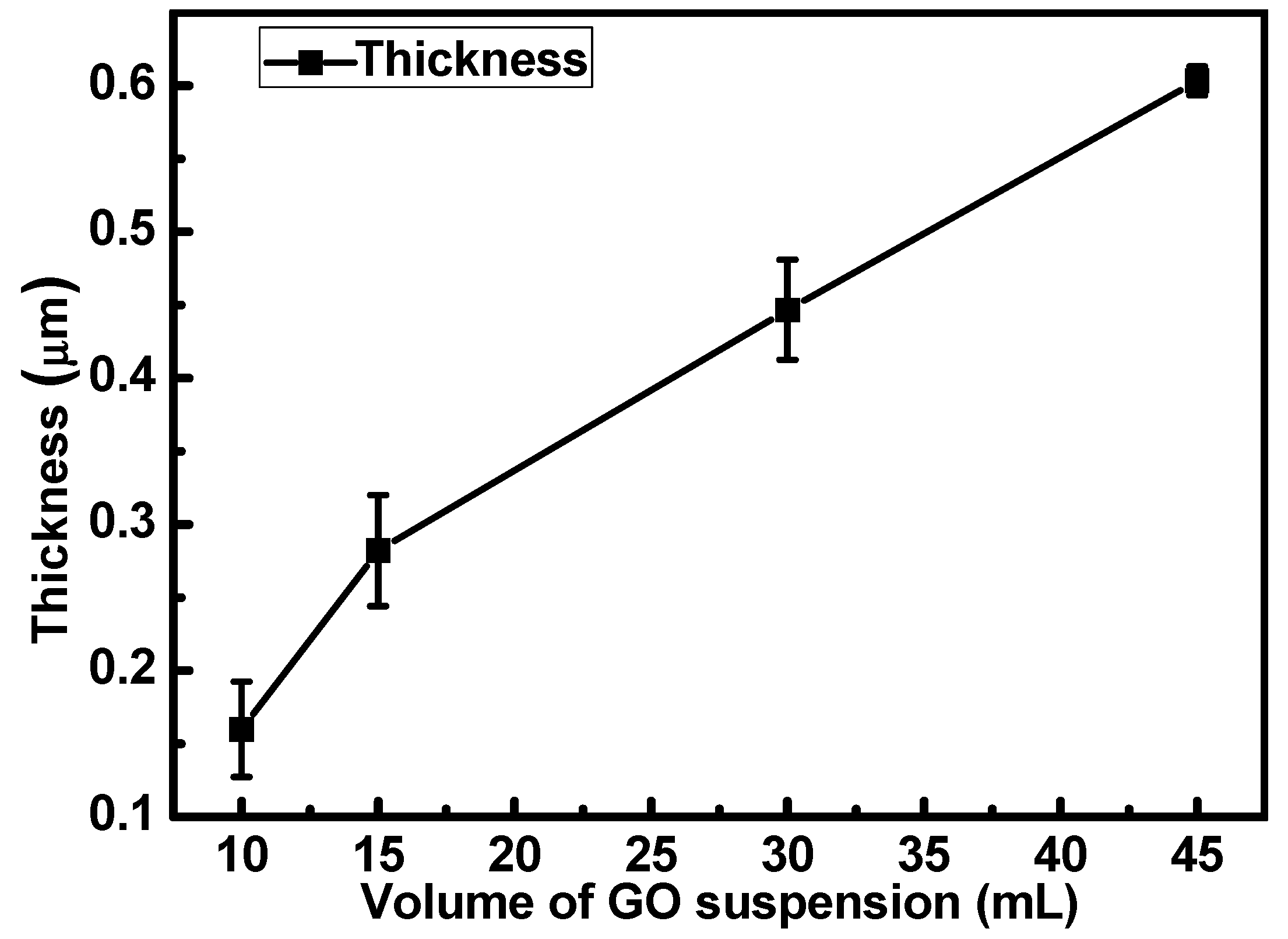
2.2. Deposition of GO Thin Films and TiO2-GO Thin Films

GO thin films were fabricated by the vacuum filtration method [47,48]. GO (10 mg) was added to 300 mL of DI water and sonicated for 1 h. The GO suspension was then filtered through a mixed cellulose ester membrane (pore size: 0.22 µm). The GO film thickness could be varied by adjusting the filtration volume of the GO suspension. To optimize the film thickness, GO films were deposited using filtration volumes of 10, 15, 30, and 45 mL. Next, the film was transferred to the PET substrate and pressed for 12 h. The ester membrane was dissolved by soaking it in acetone for 1.5–2 h, rinsing it with methanol and DI water, and drying it in an oven at 40 °C. To manufacture TiO2–GO thin films, 10 mg of GO was dispersed in 200 mL of DI water and 100 mL ethanol. After sonication for 1 h, 5 mg of TiO2 (P25, Degussa, London, UK) was added to the GO suspension. The TiO2-GO suspension was sonicated for 1.5 h.

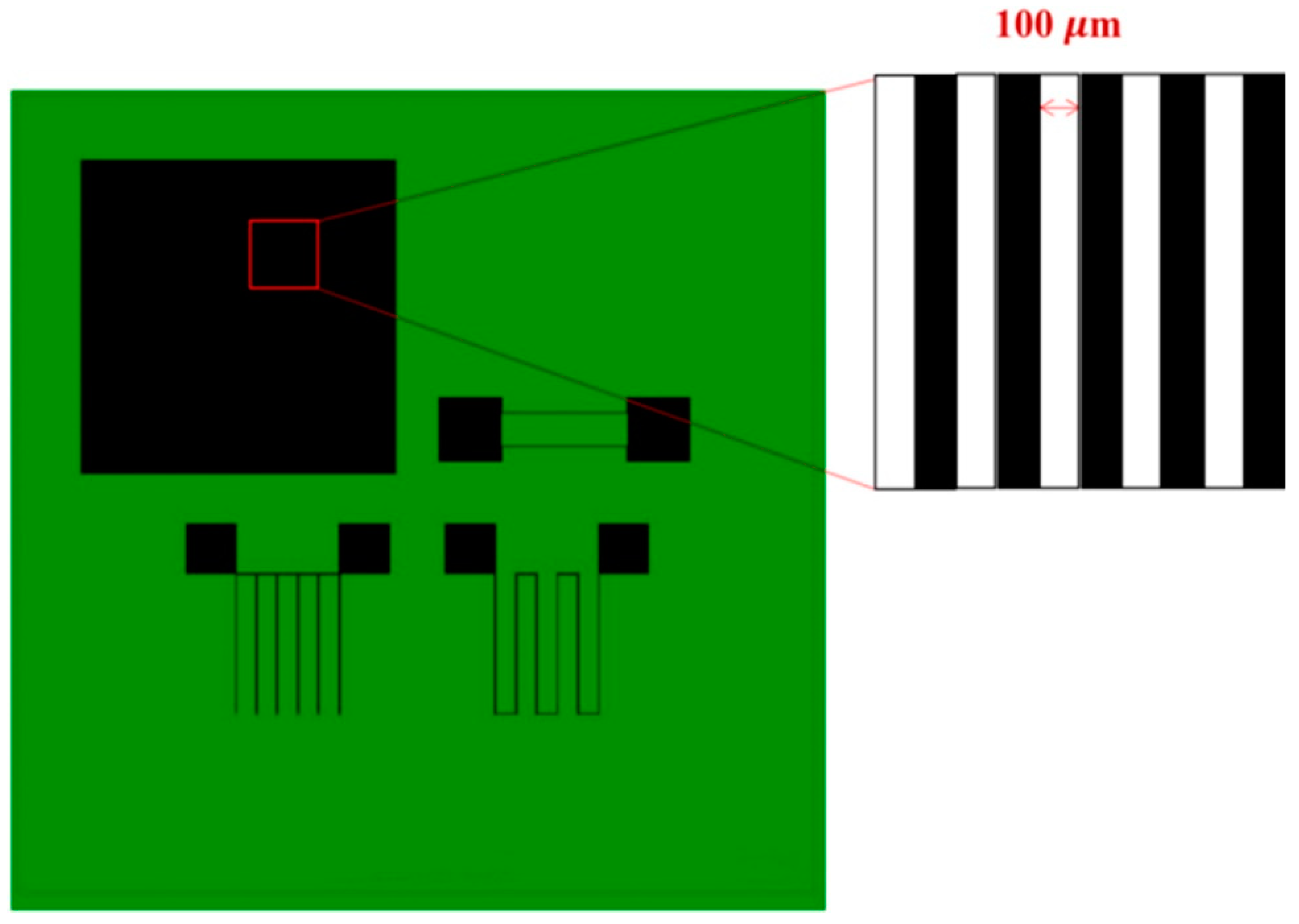
2.3. Graphene Patterning

GO and TiO2-GO films were pattered using a pulsed light system that employed spectral wavelengths of 475–1200 nm. The apparatus providing the pulsed photon energy had five energy densities: 4.5, 5.0, 5.5, 6.0, and 6.5 J/cm2. Figure 1 shows the pattern mask used in this study, which is a 5-inch mask with a Cr pattern deposited on quartz glass (thickness: 2.3 mm). The properties of the rGO thin films after reduction were examined by a four-point probe, AFM (Parker, Seoul, Korea), FE-SEM (JEOL, Tokyo, Japan), and Raman spectroscopy (Nanobase, Seoul, Korea).

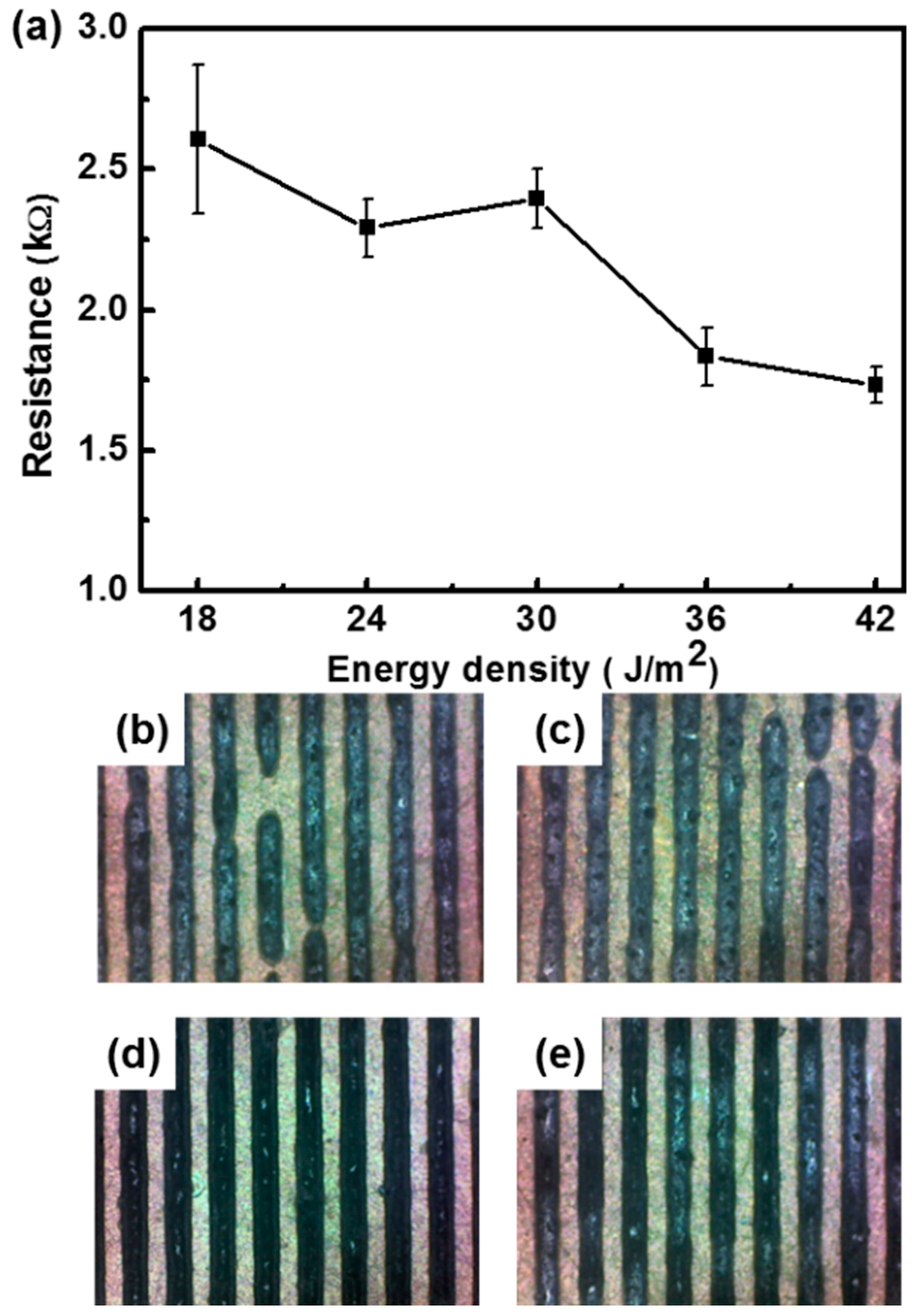
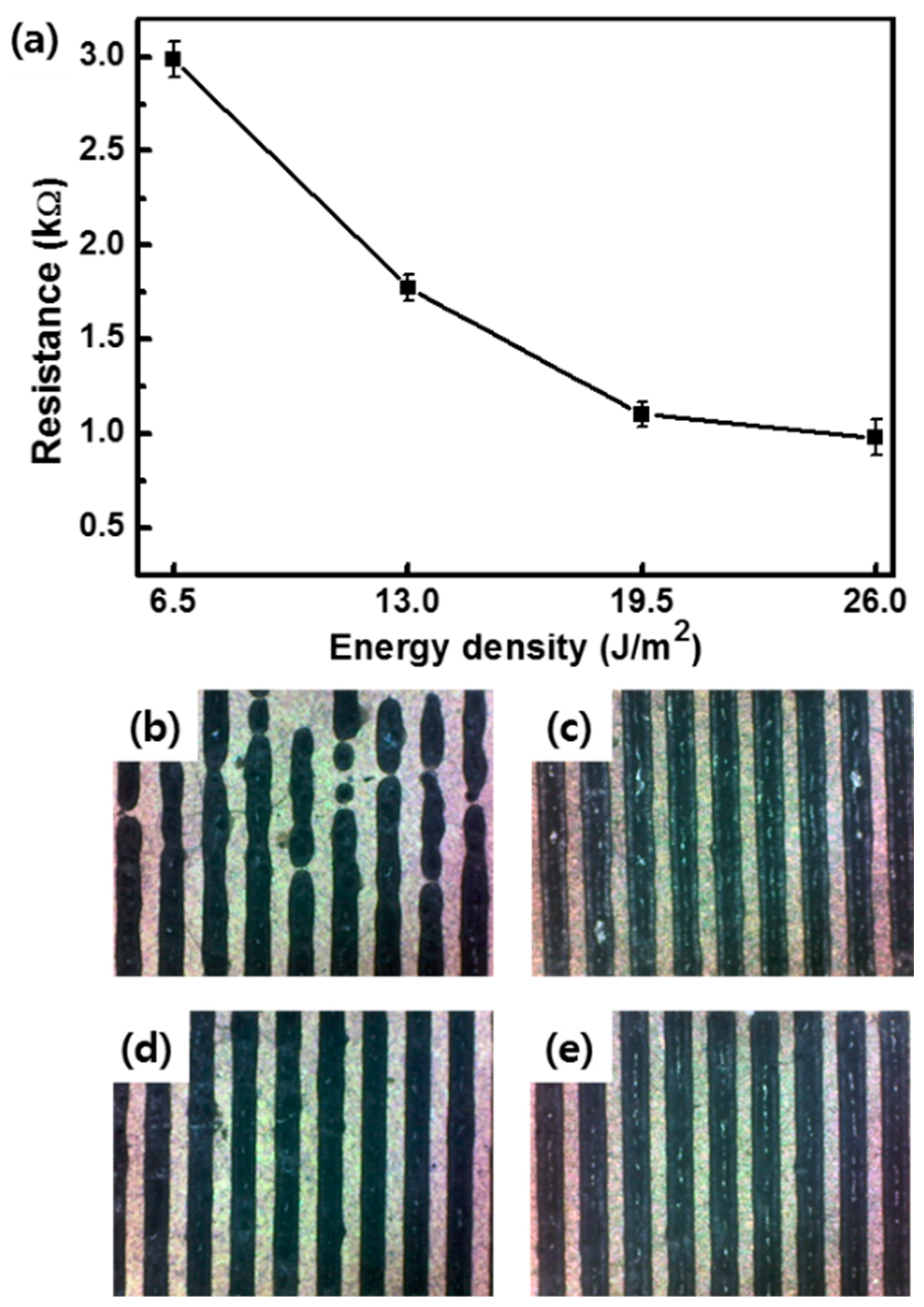
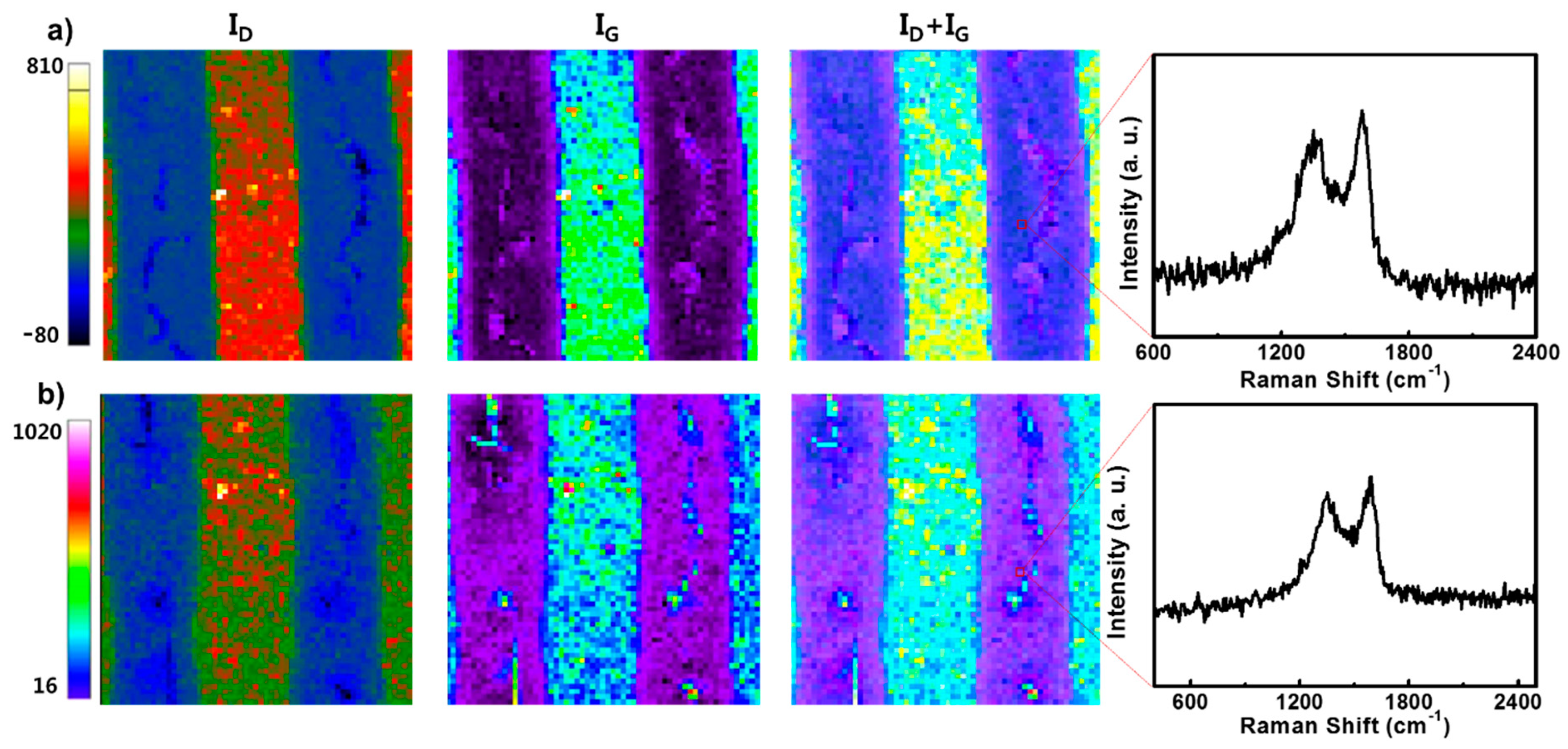
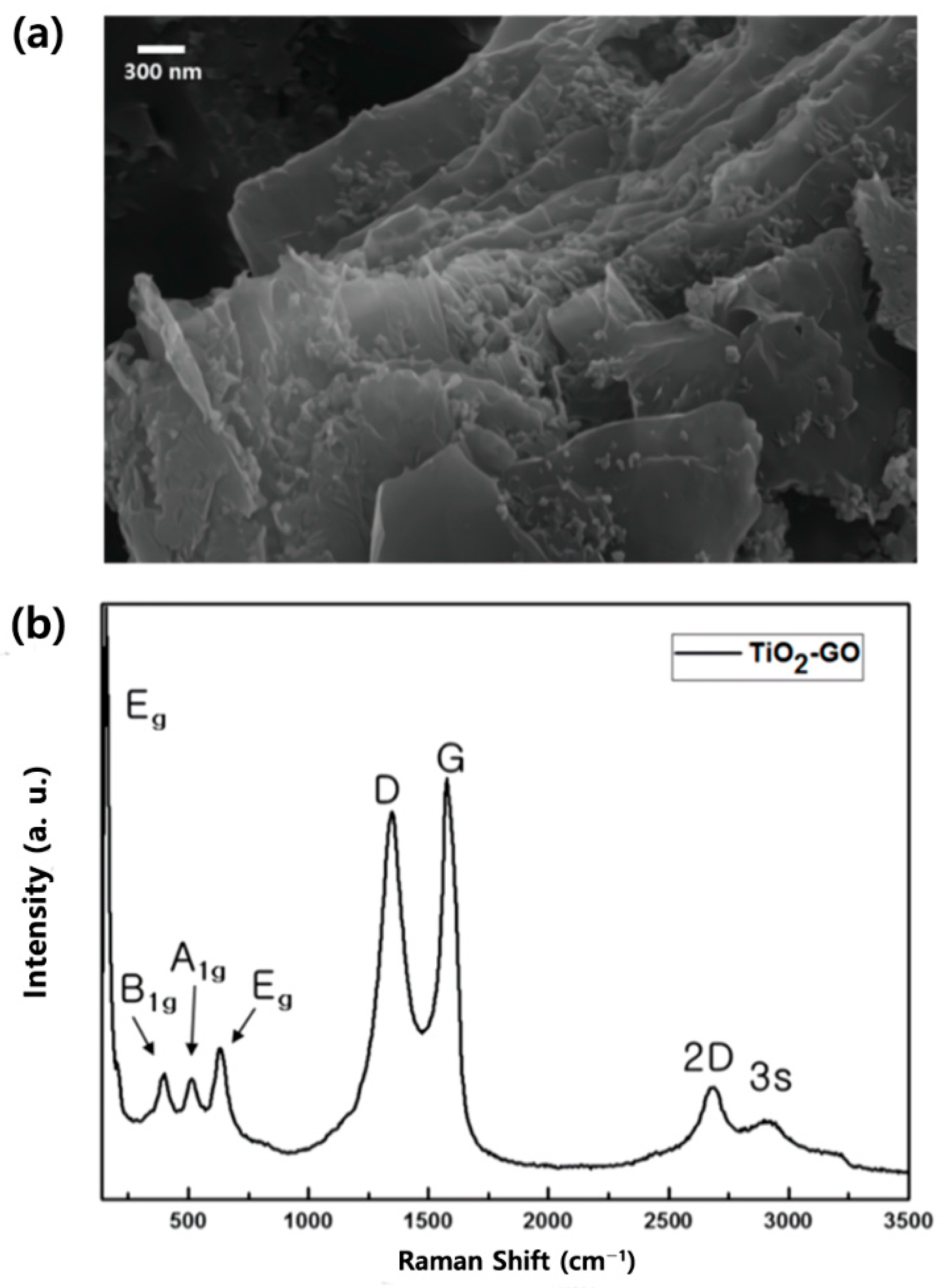
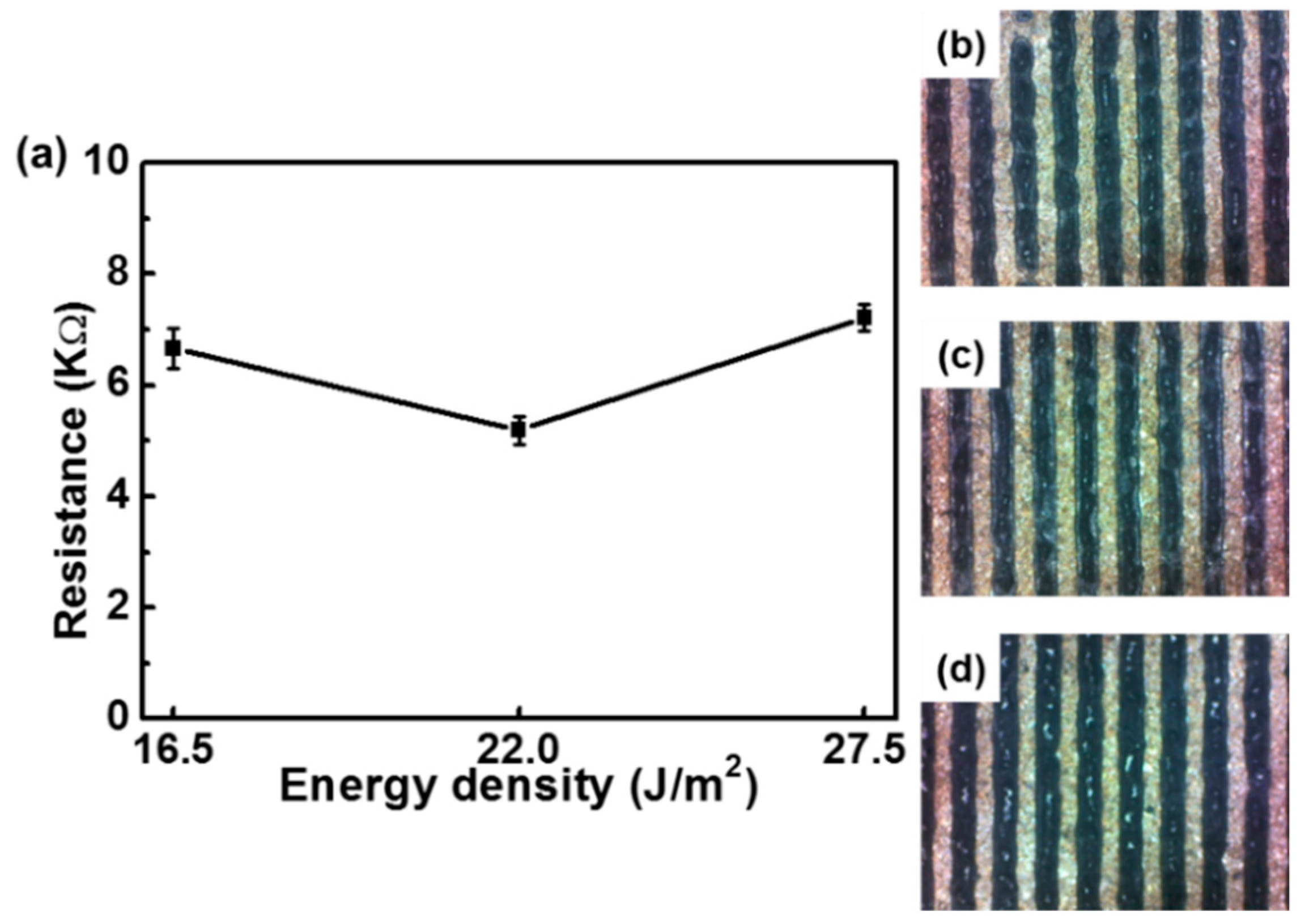
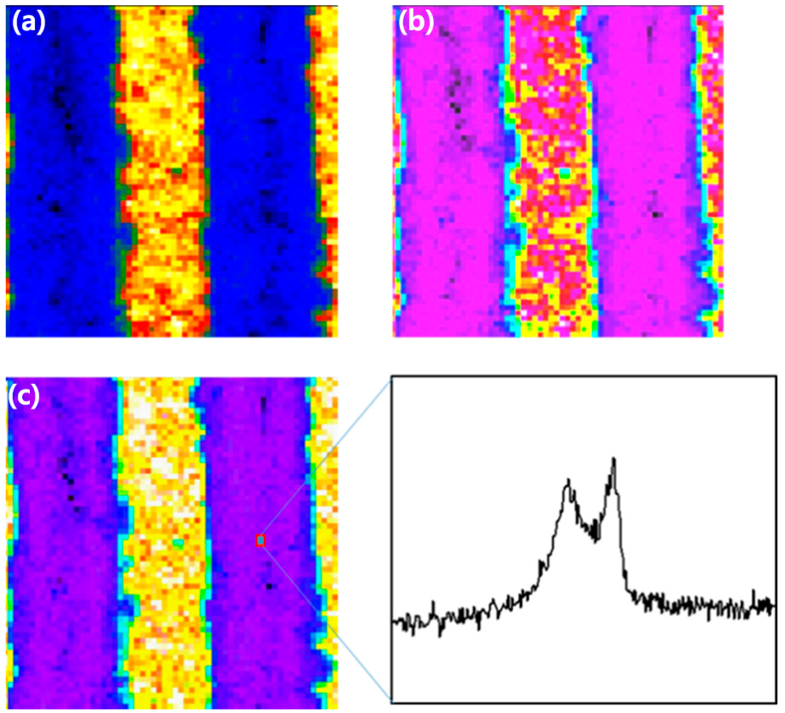
3. Results and Discussion

Photo thermal reduction is a process in which GO is reduced to produce rGO due to the thermal energy of 300 °C or more, which is generated instantaneously as photon energy and is converted into thermal energy. According to Feng et al., as the layer thickness increases, the emissive thermal energy becomes smaller in 2D nanomaterial [49,50]. Meanwhile, thermal energy transfer depends on the thickness of GO films, which is controlled by the volume expansion of GO.
Hence, it is essential to determine the optimal volume of GO suspension required to form a GO thin film with a uniform thickness by the vacuum filtration method. In this method, the film thickness depends on the filtered GO solution. The thickness of GO thin film is analyzed by AFM after filtering 10, 15, 30, and 45 mL of a 0.033 mg mL−1 GO solution (Figure 2). A linear relationship is observed between the GO film thickness and the volume of the GO suspension.
We have confirmed through previous experiments that a large amount of damage was caused by excessive thermal energy of a 0.2-μm-thick GO film. For instance, the experiment was performed with 0.45 µm films.
Figure 3 shows the patterned rGO-GO film resistance and optical image according to pulsed energy 6 J/cm2 at one time. At an energy density of less than 30 J/cm2, the reduction reaction does not even partially occur and the patterning is not successful, and it seems to be the most successful patterning when the energy density is 36 or 42 J/cm2. Meanwhile, it has a similar resistance value. Therefore, Raman mapping was measured for a more accurate analysis (Figure 4).
Figure 4 shows the Raman spectroscopy mapping of a patterned rGO-GO film irradiated with 36 or 42 J/cm2 energy density, which seems to be the most successful patterning in rGO sheet resistance and optical image.
Generally, carbon materials have a D band around 1350 cm−1 and a G band around 1580 cm−1 [51,52]. The D band is related to incomplete structural defects, and the G band is associated with E2g vibrational modes of sp2 carbons.
According to Raman mapping, the GO film is partially reduced by pulsed energy, and it can be confirmed that the D band peak and the G band peak intensity of rGO and GO are different from each other. It is confirmed that the patterned rGO-GO film was efficiently reduced when the energy density of 42 J/cm2 was irradiated (Figure 4b). Considering the sheet resistance result shown in Figure 3a, when the energy density of pulsed energy is irradiated at 36 J/cm2, the thermal budget generated by pulsed energy is used to reduce GO, and the volume expansion of GO is small due to the relatively low thermal budget. On the other hand, it predicted efficiently reduced or rapid volume expansion of the GO film when the energy density of pulsed energy is 42 J/cm2 compared to pulsed energy of 36 J/m2. As a result, it has a thermal budget capable of an efficient reduction process without damaging the rGO line when pulsed energy is irradiated at 42 J/cm2. Next, we show the result of the patterned rGO-GO film resistance and optical image according to pulsed energy 6.5 J/cm2 at one time (Figure 5).
The GO reduction reaction does not occur partially when the total irradiated energy density is 6.5 J/cm2, and rGO-GO film patterning is not successful. In comparison, it can be confirmed that the rGO-GO film patterning is relatively successful when the energy density of 19.5 J/cm2. At an energy density of 26 J/cm2, the damages appeared on the rGO line partially. Raman analysis performed each pattered rGO-GO film for precise analysis (Figure 6). In the optical image, the energy density of 19 J/cm2 seems to be the most successful rGO-GO film patterning, and when the irradiation energy density is 26 J/cm2, the rGO line seems to be defective due to an excessive thermal budget. Raman mapping results show the same results as expected in the optical image. When the energy density of 19 J/cm2 was irradiated (Figure 6a), some damage of the rGO line was observed due to the volumetric expansion of GO. However, the film type maintained. Meanwhile, it can be confirmed that the defect on the rGO line when the energy density of 26 J/cm2 was irradiated (Figure 6b) because of a decrease in adhesion to PET due to the rapid volume expansion of GO.
As a result, the damage-free rGO line is patterned by irradiating the energy density of 42 J/cm2 when the pulse energy irradiated is 6 J/cm2 can be demonstrated. However, it confirmed that the resistance of the rGO line is relatively high at 1.70 kΩ. On the other hand, the rGO line was most efficiently patterned by irradiating the energy density of 19 J/cm2 when the pulse energy irradiated is 6.5 J/cm2 because it has a low resistance of 1.10 kΩ.
TiO2 is the most commonly used photo catalysis due to its characteristics of photo catalysis performance, nontoxicity, easy availability, and long-term stability. TiO2 were excited to generate electron–hole pairs under UV (~365 nm) irradiation. The holes reacted with surface-adsorbed water to generate oxygen and protons, and on the other hand, the electrons could be successfully captured by the sp2 orbital of GO [49,50].
Figure 7 shows an FE-SEM image and Raman spectroscopy of the TiO2-GO composite. Figure 7a shows the FE-SEM image of the TiO2-GO composite. TiO2 particles been formed on GO surface. Figure 7b shows the Raman spectrum of the TiO2-GO composite. The Raman peaks observed at around 1350 cm−1 and around 1580 cm−1 can be assigned to the D band peak and G band peak, respectively. The D band is related to sp3 defect and the G band is associated to the E2g of sp2 C atom vibration mode of carbon. Furthermore, those observed at around 140 cm−1, 400 cm−1, 510 cm−1, and 640 cm−1 can be assigned to the Eg, B1g, A1g, and Eg, of the anatage phase, respectively.
Figure 8 shows the resistance and corresponding optical images of TiO2-rGO films obtained using a pulsed photon energy of 5.5 J/m2. When the energy density was below 16.5 J/m2, no partial reduction reaction occurred, and patterning was not successful. The most successful patterning was obtained when the energy density was 22 J/m2, as rGO-TiO2 line defects were observed in the optical image when the energy density was 27.5 J/m2. Notably, it indicated that the resistance increased as the irradiated energy density increased. Thus, it is considered that rGO-TiO2 line defects affect the measured resistance in the four-point probe system [25].
The Raman mapping results (Figure 9) suggest that the GO films have been reduced through pulsed energy, and the intensity of the D band peak and the G band peak are displayed differently for TiO2-rGO and TiO2-GO. However, defects were generated in the TiO2-rGO lines. In addition, unlike in the GO film, the edges of the rGO-TiO2 lines in the TiO2-GO are not linear. TiO2-GO is instantaneously heated to 300 °C or more by the pulsed photon energy, and the generated thermal energy removes oxygen-containing functional groups from the GO surface. It is likely that defects occur in the rGO-TiO2 lines owing to the difference in the thermal expansion coefficients of TiO2 and GO, resulting in lines with nonlinear edges.

4. Conclusions

In this study, rGO-GO patterning by photothermal reduction and photocatalytic reduction was examined. rGO line damage on the irradiated GO films was influenced by the pulsed photon energy as well as the total irradiation energy density. Thus, to achieve damage-free rGO line patterning, the photon energy per pulse should be considered along with the total energy density. Damage-free rGO-GO patterns were obtained by irradiating a thin GO film (thickness: 0.45 µm) using a photon energy of 6.0 J/m2 per pulse with an energy density of 42 J/m2 or a photon energy of 6.5 J/m2 per pulse with an energy density of 26 J/m2. Otherwise, it was determined that when the pulsed photon energy was irradiated at one pulse lower than the GO film, the reduction reaction of TiO2-GO happened. However, the TiO2-GO system exhibits inconsistencies owing to differences between the thermal expansion coefficients of TiO2 and GO.

Author Contributions

Conceptualization, S.P.; methodology, E.C.; formal analysis, E.C.; investigation, E.C. and S.P.; resources, E.C.; data curation, E.C.; writing—original draft preparation, E.C. and S.P.; writing—review and editing, S.P.; visualization, S.P.; supervision, S.P.; project administration, S.P.; funding acquisition, S.P. All authors have read and agreed to the published version of the manuscript.

Funding

This research was supported by Basic Science Research Program through the National Research Foundation of Korea (NRF) funded by the Ministry of Education, Science and Technology (Grant No. NRF-2019R1A2C1007670). And this work was also supported by the Technology Innovation Program (or Industrial Strategic Technology Development Program-The Development of next-generation intelligent semiconductor technology) (20012609, Atomic Layer Etching Solution and System for Real Time Process Control) funded By the Ministry of Trade, Industry & Energy (MOTIE, Korea).

Institutional Review Board Statement

Not applicable.

Informed Consent Statement

Not applicable.

Data Availability Statement

Not applicable.

Conflicts of Interest

The authors declare no conflict of interest.

References

  1. Wang, F.; Zhao, Z.; Nie, N.; Wang, F.; Zhu, W. Dynamic through-silicon-via filling process using copper electrochemical deposition at different current densities. Sci. Rep. 2017, 7, 46639. [Google Scholar] [CrossRef] [Green Version]
  2. Shen, W.-W.; Chen, K.-N. Three-dimensional integrated circuit (3D IC) key technology: Through-silicon via (TSV). Nanoscale Res. Lett. 2017, 12, 56. [Google Scholar] [CrossRef] [PubMed] [Green Version]
  3. Feng, W.; Watanabe, N.; Shimamoto, H.; Kikuchi, K.; Aoyagi, M. Methods to Reduce Thermal Stress for TSV Scaling~TSV with Novel Structure: Annular-Trench-Isolated TSV. In Proceedings of the 2015 IEEE 65th Electronic Components and Technology Conference (ECTC), San Diego, CA, USA, 26–29 May 2015; pp. 1057–1062. [Google Scholar]
  4. Kim, D.H.; Lim, S.K. Impact of Through-Silicon-via Scaling on the Wirelength Distribution of Current and Future 3D ICs. In Proceedings of the 2011 IEEE International Interconnect Technology Conference and 2011 Materials for Advanced Metallization (IITC/MAM), Dresden, Germany, 8–12 May 2011; pp. 1–3. [Google Scholar]
  5. Lu, K.H.; Zhang, X.; Ryu, S.K.; Huang, R.; Ho, P.S. Thermal Stresses Analysis of 3-D Interconnect. In Proceedings of the AIP Conference Proceedings; American Institute of Physics: College Park, MD, USA, 2009; pp. 224–230. [Google Scholar]
  6. Park, H.; Seo, H.; Kim, S.E. Characteristics of copper nitride nanolayer used in 3d cu bonding interconnects. Electron. Mater. Lett. 2021. [Google Scholar] [CrossRef]
  7. Mortazavi, B.; Shahrokhi, M.; Rabczuk, T.; Pereira, L.F.C. Electronic, optical and thermal properties of highly stretchable 2D carbon Ene-yne graphyne. Carbon 2017, 123, 344–353. [Google Scholar] [CrossRef] [Green Version]
  8. Lei, T.; Chen, X.; Pitner, G.; Wong, H.-S.P.; Bao, Z. Removable and recyclable conjugated polymers for highly selective and high-yield dispersion and release of low-cost carbon nanotubes. J. Am. Chem. Soc. 2016, 138, 802–805. [Google Scholar] [CrossRef]
  9. Park, O.-K.; Tiwary, C.S.; Yang, Y.; Bhowmick, S.; Vinod, S.; Zhang, Q.; Colvin, V.L.; Asif, S.S.; Vajtai, R.; Penev, E.S. Magnetic field controlled graphene oxide-based origami with enhanced surface area and mechanical properties. Nanoscale 2017, 9, 6991–6997. [Google Scholar] [CrossRef]
  10. Yang, Y.; Yang, X.; Zou, X.; Wu, S.; Wan, D.; Cao, A.; Liao, L.; Yuan, Q.; Duan, X. Ultrafine graphene nanomesh with large on/off ratio for high-performance flexible biosensors. Adv. Funct. Mater. 2017, 27, 1604096. [Google Scholar] [CrossRef]
  11. Yang, M.K.; Lee, J.K. CNT/AgNW Multilayer electrodes on flexible organic solar cells. Electron. Mater. Lett. 2020, 16, 573–578. [Google Scholar] [CrossRef]
  12. Kim, S.; Lee, K.-H.; Lee, J.-Y.; Kim, K.-K.; Choa, Y.-H.; Lim, J.-H. Single-walled carbon nanotube-based chemi-capacitive sensor for hexane and ammonia. Electron. Mater. Lett. 2019, 15, 712–719. [Google Scholar] [CrossRef]
  13. Choi, E.; Kim, D.; Lee, I.; Chae, S.J.; Kim, A.; Pyo, S.G.; Yoon, S. SnO2-graphene nanocomposite free-standing film as anode in lithium-ion batteries. Electron. Mater. Lett. 2015, 11, 836–840. [Google Scholar] [CrossRef]
  14. Chen, X.Y.; Akinwande, D.; Lee, K.J.; Close, G.F.; Yasuda, S.; Paul, B.C.; Fujita, S.; Kong, J.; Wong, H.S.P. Fully integrated graphene and carbon nanotube interconnects for gigahertz high-speed cmos electronics. IEEE Trans. Electron. Dev. 2010, 57, 3137–3143. [Google Scholar] [CrossRef]
  15. Ghosh, K.; Ranjan, N.; Verma, Y.K.; Tan, C.S. Graphene-CNT hetero-structure for next generation interconnects. RSC Adv. 2016, 6, 53054–53061. [Google Scholar] [CrossRef]
  16. Maffucci, A.; Miano, G. Number of conducting channels for armchair and zig-zag graphene nanoribbon interconnects. IEEE Trans. Nanotechnol. 2013, 12, 817–823. [Google Scholar] [CrossRef]
  17. Hwang, U.G.; Kim, K.; Kim, W.; Shin, W.H.; Seo, W.-S.; Lim, Y.S. Thermoelectric transport properties of interface-controlled p-type bismuth antimony telluride composites by reduced graphene oxide. Electron. Mater. Lett. 2019, 15, 605–612. [Google Scholar] [CrossRef]
  18. Kim, J.; Choi, E.; Lee, I.; Kim, D.; Han, S.; Pyo, S.G.; Yoon, S. Investigation of the charge-storage behavior of electrochemically activated graphene oxide on supercapacitor electrodes in acidic electrolyte. Electron. Mater. Lett. 2017, 13, 434–441. [Google Scholar] [CrossRef]
  19. Choi, E.; Kim, J.; Cui, Y.; Choi, K.; Gao, Y.; Han, S.; Pyo, S.G.; Yoon, S. Effect of the graphene oxide reduction temperature on supercapacitor performance. Electron. Mater. Lett. 2017, 13, 324–329. [Google Scholar] [CrossRef]
  20. Nardecchia, S.; Carriazo, D.; Ferrer, M.L.; Gutiérrez, M.C.; del Monte, F. Three dimensional macroporous architectures and aerogels built of carbon nanotubes and/or graphene: Synthesis and applications. Chem. Soc. Rev. 2013, 42, 794–830. [Google Scholar] [CrossRef]
  21. Toh, S.Y.; Loh, K.S.; Kamarudin, S.K.; Daud, W.R.W. Graphene production via electrochemical reduction of graphene oxide: Synthesis and characterisation. Chem. Eng. J. 2014, 251, 422–434. [Google Scholar] [CrossRef]
  22. Qi, Z.J.; Rodríguez-Manzo, J.A.; Hong, S.J.; Park, Y.W.; Stach, E.A.; Drndić, M.; Johnson, A.C. Direct electron beam patterning of sub-5nm monolayer graphene interconnects. In Proceedings of the SPIE Advanced Lithography; International Society for Optics and Photonics: Bellingham, WA, USA, 2013; p. 86802. [Google Scholar]
  23. Wei, Z.J.; Hou, Y.X.; Jiang, C.; Liu, H.Y.; Chen, X.R.; Zhang, A.Y.; Liu, Y.X. Graphene enhanced electrical properties of polyethylene blends for high-voltage insulation. Electron. Mater. Lett. 2019, 15, 582–594. [Google Scholar] [CrossRef]
  24. Li, Y.; Zhao, Y.; Cheng, H.; Hu, Y.; Shi, G.; Dai, L.; Qu, L. Nitrogen-doped graphene quantum dots with oxygen-rich functional groups. J. Am. Chem. Soc. 2011, 134, 15–18. [Google Scholar] [CrossRef]
  25. Huang, L.; Liu, Y.; Ji, L.-C.; Xie, Y.-Q.; Wang, T.; Shi, W.-Z. Pulsed laser assisted reduction of graphene oxide. Carbon 2011, 49, 2431–2436. [Google Scholar] [CrossRef]
  26. Pei, S.; Cheng, H.-M. The reduction of graphene oxide. Carbon 2012, 50, 3210–3228. [Google Scholar] [CrossRef]
  27. Park, S.; An, J.; Potts, J.R.; Velamakanni, A.; Murali, S.; Ruoff, R.S. Hydrazine-reduction of graphite-and graphene oxide. Carbon 2011, 49, 3019–3023. [Google Scholar] [CrossRef]
  28. Prezioso, S.; Perrozzi, F.; Donarelli, M.; Stagnini, E.; Treossi, E.; Palermo, V.; Santucci, S.; Nardone, M.; Moras, P.; Ottaviano, L. Dose and wavelength dependent study of graphene oxide photoreduction with VUV Synchrotron radiation. Carbon 2014, 79, 478–485. [Google Scholar] [CrossRef]
  29. Prezioso, S.; Perrozzi, F.; Donarelli, M.; Bisti, F.; Santucci, S.; Palladino, L.; Nardone, M.; Treossi, E.; Palermo, V.; Ottaviano, L. Large area extreme-UV lithography of graphene oxide via spatially resolved photoreduction. Langmuir 2012, 28, 5489–5495. [Google Scholar] [CrossRef]
  30. Cullis, A.G.; Webber, H.C.; Chew, N.G.; Poate, J.M.; Baeri, P. Transitions to defective crystal and the amorphous state induced in elemental si by laser quenching. Phys. Rev. Lett. 1982, 49, 219–222. [Google Scholar] [CrossRef]
  31. Pei, L.M.; Li, Y.F. Rapid and efficient intense pulsed light reduction of graphene oxide inks for flexible printed electronics. RSC Adv. 2017, 7, 51711–51720. [Google Scholar] [CrossRef] [Green Version]
  32. Al-Hamry, A.; Kang, H.; Sowade, E.; Dzhagan, V.; Rodriguez, R.D.; Müller, C.; Zahn, D.R.T.; Baumann, R.R.; Kanoun, O. Tuning the reduction and conductivity of solution-processed graphene oxide by intense pulsed light. Carbon 2016, 102, 236–244. [Google Scholar] [CrossRef]
  33. de Lima, B.S.; Bernardi, M.I.B.; Mastelaro, V.R. Wavelength effect of ns-pulsed radiation on the reduction of graphene oxide. Appl. Surf. Sci. 2020, 506, 144808. [Google Scholar] [CrossRef]
  34. Filice, S.; D’Angelo, D.; Spanò, S.F.; Compagnini, G.; Sinatra, M.; D’Urso, L.; Fazio, E.; Privitera, V.; Scalese, S. Modification of graphene oxide and graphene oxide–TiO2 solutions by pulsed laser irradiation for dye removal from water. Mater. Sci. Semicond. Process. 2016, 42, 50–53. [Google Scholar] [CrossRef]
  35. Menazea, A.; Ahmed, M.K. Silver and copper oxide nanoparticles-decorated graphene oxide via pulsed laser ablation technique: Preparation, characterization, and photoactivated antibacterial activity. Nano-Struct. Nano-Objects 2020, 22, 100464. [Google Scholar] [CrossRef]
  36. Sachan, R.; Gupta, S.; Narayan, J. Nonequilibrium structural evolution of Q-carbon and interfaces. ACS Appl. Mater. Interfaces 2020, 12, 1330–1338. [Google Scholar] [CrossRef] [PubMed]
  37. Trusovas, R.; Ratautas, K.; Račiukaitis, G.; Barkauskas, J.; Stankevičienė, I.; Niaura, G.; Mažeikienė, R. Reduction of graphite oxide to graphene with laser irradiation. Carbon 2013, 52, 574–582. [Google Scholar] [CrossRef]
  38. Sokolov, D.A.; Shepperd, K.R.; Orlando, T.M. Formation of graphene features from direct laser-induced reduction of graphite oxide. J. Phys. Chem. Lett. 2010, 1, 2633–2636. [Google Scholar] [CrossRef]
  39. Gupta, S.; Narayan, J. Non-equilibrium processing of ferromagnetic heavily reduced graphene oxide. Carbon 2019, 153, 663–673. [Google Scholar] [CrossRef]
  40. Gupta, S.; Narayan, J. Reduced graphene oxide/amorphous carbon P–N junctions: Nanosecond laser patterning. ACS Appl. Mater. Interfaces 2019, 11, 24318–24330. [Google Scholar] [CrossRef] [PubMed]
  41. Sokolov, D.A.; Rouleau, C.M.; Geohegan, D.B.; Orlando, T.M. Excimer laser reduction and patterning of graphite oxide. Carbon 2013, 53, 81–89. [Google Scholar] [CrossRef]
  42. Saini, A.; Kumar, A.; Anand, V.K.; Sood, S.C. Synthesis of graphene oxide using modified hummer’s method and its reduction using hydrazine hydrate. Int. J. Eng. Trends Technol. 2016, 40, 67–71. [Google Scholar] [CrossRef]
  43. Fan, W.; Lai, Q.; Zhang, Q.; Wang, Y. Nanocomposites of TiO2 and reduced graphene oxide as efficient photocatalysts for hydrogen evolution. J. Phys. Chem. C 2011, 115, 10694–10701. [Google Scholar] [CrossRef]
  44. Moraes, F.C.; Freitas, R.G.; Pereira, R.; Gorup, L.F.; Cuesta, A.; Pereira, E.C. Coupled electronic and morphologic changes in graphene oxide upon electrochemical reduction. Carbon 2015, 91, 11–19. [Google Scholar] [CrossRef] [Green Version]
  45. Kawahara, T.; Konishi, Y.; Tada, H.; Tohge, N.; Nishii, J.; Ito, S. A patterned TiO2 (anatase)/TiO2 (rutile) bilayer-type photocatalyst: Effect of the anatase/rutile junction on the photocatalytic activity. Angew. Chem. 2002, 114, 2935–2937. [Google Scholar] [CrossRef]
  46. Shahriary, L.; Athawale, A.A. Graphene oxide synthesized by using modified hummers approach. Int. J. Renew. Energy Environ. Eng. 2014, 2, 58–63. [Google Scholar]
  47. Wang, P.; Wang, J.; Ming, T.; Wang, X.; Yu, H.; Yu, J.; Wang, Y.; Lei, M. Dye-sensitization-induced visible-light reduction of graphene oxide for the enhanced TiO2 photocatalytic performance. ACS Appl. Mater. Interfaces 2013, 5, 2924–2929. [Google Scholar] [CrossRef]
  48. Eda, G.; Fanchini, G.; Chhowalla, M. Large-area ultrathin films of reduced graphene oxide as a transparent and flexible electronic material. Nat. Nanotechnol. 2008, 3, 270–274. [Google Scholar] [CrossRef]
  49. Tung, V.C.; Allen, M.J.; Yang, Y.; Kaner, R.B. High-throughput solution processing of large-scale graphene. Nat. Nanotechnol. 2009, 4, 25. [Google Scholar] [CrossRef]
  50. Feng, F.; Guo, H.; Li, D.; Wu, C.; Wu, J.; Zhang, W.; Fan, S.; Yang, Y.; Wu, X.; Yang, J. Highly efficient photothermal effect by atomic-thickness confinement in two-dimensional ZrNCl nanosheets. ACS Nano 2015, 9, 1683–1691. [Google Scholar] [CrossRef]
  51. Park, J.; Xiong, W.; Gao, Y.; Qian, M.; Xie, Z.; Mitchell, M.; Zhou, Y.; Han, G.; Jiang, L.; Lu, Y. Fast growth of graphene patterns by laser direct writing. Appl. Phys. Lett. 2011, 98, 123109. [Google Scholar] [CrossRef]
  52. Park, M.; Choi, H.; Park, Y.; Lee, W.; Lee, J.; Jeon, M. Fabrication and characterization of graphene-based electrochemical sensors for glucose measurement. J. Nanosci. Nanotechnol. 2015, 15, 7891–7894. [Google Scholar] [CrossRef]
Figure 1. Pattern mask design: line pattern and cube pattern.
Coatings 11 01042 g001
Figure 2. Thicknesses of GO films obtained from various volumes of GO suspension.
Coatings 11 01042 g002
Figure 3. The patterned rGO-GO sheet resistance and optical image according to pulsed energy 6 J/cm2 at one time. Sheet resistance (a), optical images of 24 J/m2 (b), 30 J/m2 (c), 36 J/m2 (d), and 42 J/m2 (e).
Coatings 11 01042 g003
Figure 4. Raman mapping of (a) energy density is 36 J/cm2, (b) energy density is 42 J/cm2 (300 × 300 μm2).
Coatings 11 01042 g004
Figure 5. The patterned rGO-GO sheet resistance and optical image according to pulsed energy 6.5 J/cm2 at one time. Sheet resistance (a), optical images of 6.5 J/m2 (b), 13 J/m2 (c), 19.5 J/m2 (d), and 26 J/m2 (e).
Coatings 11 01042 g005
Figure 6. Raman mapping of (a) energy density is 19 J/cm2, (b) energy density is 26 J/cm2 (300 × 300 μm2).
Coatings 11 01042 g006
Figure 7. (a) FE-SEM image and (b) Raman spectroscopy of TiO2-GO composite.
Coatings 11 01042 g007
Figure 8. The patterned TiO2-rGO sheet resistance and optical image according to pulsed energy 5.5 J/cm2 at one time. Sheet resistance (a), optical images of 16.5 J/m2 (b), 22.0 J/m2 (c), and 27.5 J/m2 (d).
Coatings 11 01042 g008
Figure 9. Raman mapping of energy density is 22 J/m2: (a) ID, (b) IG, (c) ID + IG.
Coatings 11 01042 g009
Publisher’s Note: MDPI stays neutral with regard to jurisdictional claims in published maps and institutional affiliations.

