Article

Preparation of Double-Layer Crossed Silver Nanowire Film and Its Application to OLED

1
School of Electronic and Information Engineering, Zhongshan Institute, University of Electronic Science and Technology of China, Zhongshan 528402, China
2
School of Physics, University of Electronic Science and Technology of China, Chengdu 610054, China
*
Author to whom correspondence should be addressed.
Coatings 2022, 12(1), 26; https://doi.org/10.3390/coatings12010026
Submission received: 18 November 2021 / Revised: 20 December 2021 / Accepted: 21 December 2021 / Published: 27 December 2021
(This article belongs to the Topic Inorganic Thin Film Materials)

Abstract

:
Ordered silver nanowire (AgNW) film can effectively reduce the density of nodes, reduce the roughness of the film, and increase its conductivity and transmittance. In this paper, a double-layer crossed AgNW grid film was prepared by the auxiliary stirring method. The average transmittance of the double-layer crossed AgNW grid film was found to be 80% in the 400–1000 nm band, with a square resistance of 35 Ω/sq. As a transparent conductive anode material, the ordered AgNW film was applied to fabricate a flexible green organic light-emitting diode (OLED). The experimental results showed that the threshold voltage of the OLED was only 5 V and the maximum luminance was 1500 cd/m2.

1. Introduction

With the popularity of intelligent and portable concepts, people’s requirements for electronic devices are constantly improving. With the rapid development of material science and electronic technology, wearable devices and flexible foldable electronic devices based on flexible display screens have gradually moved from conceptual models to physical objects.
Indium tin oxide (ITO) is a traditional organic light-emitting diode (OLED) material. Its high optical transmittance and low square resistivity in the whole visible spectrum make it the standard for most modern applications. At the same time, ITO has a high work function (~4.8 ev), and thus, is an ideal material for the OLED anode. However, ITO has the following disadvantages: (1) as a rare metal material, indium resource has a low storage capacity in the crust, which leads to the high price of ITO; (2) the sputtering process of ITO needs higher temperature, so the choice of substrate material is limited by heat resistance; (3) ITO is a brittle material with poor mechanical properties, so it is not suitable for use as the component material of flexible devices; (4) the low work function of ITO can not meet the needs of people for flexible wearable devices. The future production and application of organic semiconductor devices based on ITO will be hindered. Therefore, there is an urgent need to develop a low-cost, flexible, simple and large-scale alternative material similar to ITO. Graphene [1,2,3,4,5], conductive polymers [6,7,8], carbon nanotubes [9] and metal nanowires [10,11,12,13,14] (Au, Ag, Cu, etc.) have great potential applications [15,16] in the field of flexible transparent electrodes due to their excellent photoelectric and mechanical properties.
Because of its simple preparation technology, suitability for mass production and relatively low price, metal nanowires have attracted great attention. At the same time, the methods of film preparation are diversified and easy to implement, and the film has excellent light transmittance and conductivity, which makes it one of the most promising materials for replacing ITO. Silver nanowire (AgNW) has great advantages in terms of price and performance. The light transmittance and conductivity of flexible transparent conductive film (TCF) prepared by AgNW are close to the ITO level. Therefore, in this study, we chose AgNW as the substitute material of ITO.
AgNW can be deposited on glass or plastic substrates by drop coating [17,18], vacuum filtration [19], Meyer stick coating [20] and spin coating [21,22] methods to form randomly arranged nanowire networks. However, the disordered nanowire films prepared by these methods will have three or more nanowires superimposed on each other; thus, they will have high conductivity and large surface roughness, which will affect the contact with the upper functional layer in the process of preparing devices, and the light transmittance of the films will be poor.
It is still challenging to prepare macroscopic and anisotropic TCF nanowires at the nanoscale. Nowadays, an external driving force is mainly used. In the assembly process, the nanowires are unidirectionally arranged by the unidirectional force, and then the substrate is used to receive the aligned nanowires. According to the differences in unidirectional force, the process can be divided into dielectrophoresis-driven assembly [23], electrostatic-force-driven assembly [24,25], magnetic-force-driven assembly [26,27], shear-force-driven assembly [28,29] and surface-tension-driven assembly [30]. Theoretically, shear force is considered to be the most promising method to obtain planar uniaxial films assembled from nanowires [31].
In the process of shear force assembly, different treatment methods of the substrate will have a great influence on the experimental results. Because the movement of nanowires in the alignment process is greatly affected by the friction of the film surface, and the friction force depends on the chemical modification of the substrate surface, the friction and adhesion of the substrate surface with a methyl group at the end are poor [32] and the nanowires are arranged in order along the direction of liquid motion due to the small friction; however, due to their poor surface adhesion, nanowires attached to the substrate surface a little, and the density of the assembled nanowires is lower. However, the base modified by the amino group has high friction and adhesion, which is the most suitable substrate material for AgNW assembly driven by shear force.
Ordered silver nanowire (AgNW) film can effectively reduce the density of nodes, reduce the roughness of the film and increase its conductivity and transmittance. In this paper, AgNWs were assembled in solution, in an orderly manner, by the shear force generated by the rotation and stirring of the tiles. The two-step method was used to prepare the single layer and ordered AgNW films, which were then rotated 90 degrees to prepare the transparent conductive thin film composed of AgNWs with a double-cross arrangement. We used polyethyleneimine (PEI) to modify the surface of Polyethylene terephthalate (PET) substrate to enhance its surface friction and adhesion, which provided the possibility for the orderly deposition of AgNWs.
In this study, we innovatively used a two-step stirring method to obtain cross-silver nanowire transparent conductive films. This effectively reduced the node density on the film and increased the conductivity of the film without affecting its light transmittance. By sputtering a layer of MoS2 on the surface of the film, we could prevent the oxidation of silver nanowires in the air and ensure the stability of the device. At the same time, MoS2 was able to increase the work function of the film and play a positive role in reducing the starting voltage of the device. The films prepared by magnetron sputtering were found to have good stability and uniformity, and the sputtering process did not affect the substrate at low temperature.

2. Experimental and Results

Up to now, many synthesis methods have been developed for AgNWs, which can be roughly divided into four categories: template methods [25], electrochemical methods [26], wet chemical methods [27], and poly methods [28]. However, the preparation of large-scale AgNWs with controllable morphologies is still a difficult problem. This is also a bottleneck that restricts the further development of AgNW-based FTCF.

2.1. Hydrophilic Treatment of the PET Substrate

PET film has excellent mechanical and heat resistance properties, and is widely used in the field of photoelectric devices and plastic film packaging. It has been shown that PET film can be used stably at 120 °C and has excellent friction resistance, bending resistance, high transparency and non-toxicity, is tasteless and is suitable for the preparation of flexible transparent conductive film. However, because of the lack of strong polar groups on PET’s surface, it has poor hydrophilicity, low surface roughness and poor friction with nanowires, which is not conducive to the adhesion of nanowires.
In this experiment, PET film was purchased Vigon Technology of China (Hefei, China) and its thickness was about 188 μm. In order to make AgNWs easier to attach to the PET substrate, it is necessary to improve the hydrophilicity of the PET substrate. Common surface modification methods include chemical grafting, ultraviolet irradiation, high energy radiation, plasma treatment and surface ozone treatment. The most commonly used method for improving the hydrophilicity of the surface of the PET substrate is to change the friction and hydrophilicity of the surface by ultraviolet irradiation, then soak the substrate with a mixture of sulfuric acid and hydrogen peroxide with a volume ratio of 7:3 to hydroxyl the surface of the PET substrate. The adsorption capacity of the hydroxylation substrate to AgNWs is weak, so it is necessary to use aminopropyl triethoxysilane (APTES) solution to aminate the substrate. In this study, the surface of PET was treated by ultraviolet (UV) irradiation and chemical grafting. We tested the contact angle of the PET substrate before and after UV irradiation. Figure 1a shows the PET substrate without UV irradiation. The contact angle of the attached droplets was 54 degrees, while the contact angle of the droplets on the top was 24 degrees after 15 min of UV irradiation (as shown in Figure 1b). The contact angle is closely related to the hydrophilicity of the material, and the larger the contact angle, the smaller the hydrophilicity. It can be seen from the experiment that the hydrophilic properties of the PET substrate after UV irradiation were improved obviously, the binding force between the substrate and amino group was increased and the surface of the film was more easily aminated.

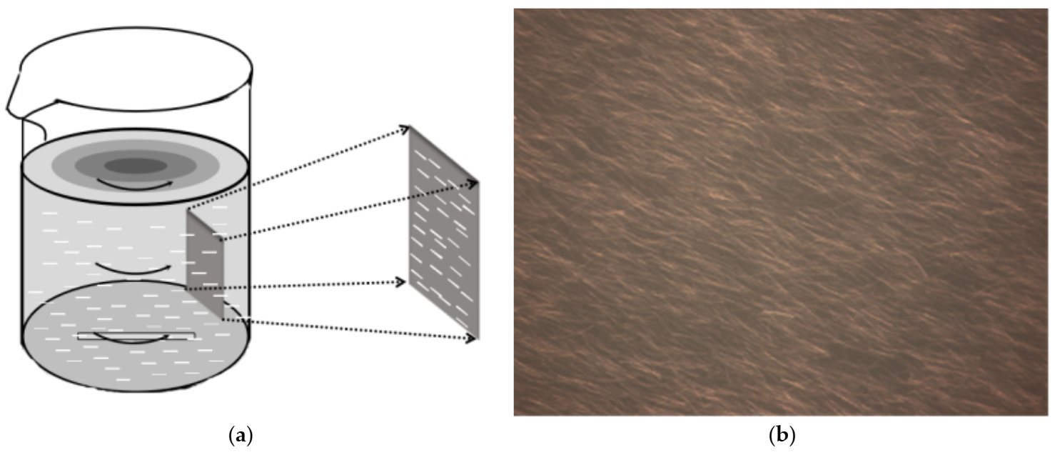
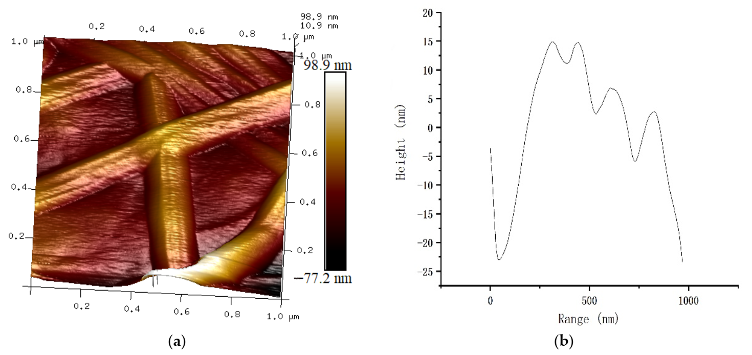
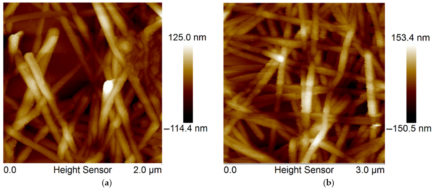
2.2. Preparation of Ordered Silver Nanowire Film

The ethylene glycol solution of AgNWs was purchased from Vigon Technology, China. The average diameter of the AgNWs was about 25 nm and its length was approximately 20–30 μm. AgNWs’ assembly was driven by shear force, and the water was rotated in the same direction by stirring. With the help of ethylene glycol flow, the AgNWs in the solution were arranged parallel to the flow direction and attached to the substrate. The schematic diagram is shown in Figure 2a. First, we cut the glass with the size of 2 cm × 8 cm, and then cleaned it with detergent, acetone and ethanol for 10 min. We pasted the 2 cm × 2 cm double-sided tape on the bottom of one side of the paste, and then attached a 2 cm × 2 cm heat release tape on the double-sided tape and pasted the aminated PET film on the heat release tape with its front facing outward. The purpose of heat release tape was to remove the PET film after the experiment. We poured 200 mL ethylene glycol solution into the beaker, added a magnetic rotor of 3 cm length, and then we dropped 5 mL 0.5 mg/mL AgNW solution into the solution, placed the beaker in the center of the magnetic stirrer, and stirred for 5 min at 300 r/min, so that the AgNWs were arranged in the direction of the ethylene glycol flow in the solution. With a self-made iron stand, we clamped the upper end of the glass sheet, and slowly immersed the end with PET film, perpendicular to the surface of the solution, into the ethylene glycol solution, with the PET side facing the center of the vortex. We adjusted the rotation speed of the magnetic rotor to 400 r/min, and after stirring for a period of time, took out the glass sheet, washed the PET side in deionized water with running water for 1 min, removed the AgNWs that were not firmly attached on the surface, and then blow dried the solution with nitrogen to obtain the uniaxial arrangement of AgNW film (as shown in Figure 2b).
In Figure 3, it is shown that the nanowire density of the AgNW film after UV irradiation was significantly higher than that of the PET film without UV irradiation under the same stirring conditions. It can be seen that before the amination of the PET film, the UV irradiation on the film was conducive to its amination, which was more conducive to the subsequent assembly of AgNWs.
The glass sheet of PET substrate with single-layer ordered AgNWs was placed on the heating table at 100 °C and the PET substrate was peeled off from the glass after the heat release adhesive tape lost its adhesion. The removed PET substrate was placed in the UV cleaning machine again and exposed to UV for 5 min with the face up. After UV irradiation, the PET substrate was completely immersed in the prepared PEI solution and removed after 30 min. The PET substrate was pasted on the glass and rotated at 90 degrees, in contrast to the preparation of the single-layer film. Then, the upper end of the glass sheet was clamped with an iron stand, and the end was slowly immersed—with the PET film perpendicular to the surface of the solution—into the ethylene glycol solution, with the PET side facing the center of the vortex. After stirring for a period of time, the glass sheet was taken out, PET side was washed with running water in deionized water for 1 min, the AgNWs that were not firmly attached onto the surface were removed, and then the solution was blow dried with nitrogen. Double-layered AgNW film with a cross arrangement could be obtained (as shown in Figure 3c). The obtained double-layer film was placed on a powder tablet press and pressed for 10 s under 30 tons of pressure to make the double-layer AgNW film have full contact, and thus, increase its conductivity.
In order to reflect the properties of the cross ordered AgNW films, we measured the transmittance and conductivity of the films. The transmittance of the film is shown in Figure 4. The average transmittance of the single-layer ordered AgNW transparent film was 87% in the 400–1000 nm band, while the average transmittance of the TCF of the double-layer crossed AgNWs was 80% in the 400–1000 nm band. We measured the conductivity of the film by measuring the square resistance. Under the optimal conditions, the TCF square resistance of the ordered AgNWs was 35 Ω/sq. In this case, the roughness of the silver nanowire film was 33 nm and the average thickness was about 46 nm.
In order to further understand the surface morphology of the ordered AgNW films, we characterized the double-layer AgNW films by atomic force microscopy (AFM, Bruker, Beijing and China) (as shown in Figure 5), and the three dimensional (3D) image is shown in Figure 5a. It can be seen that in the range of 1 μm, the AgNWs were arranged in order, the multi nanowires were embedded in each other, and the contact between AgNWs was good. At the same time, we found that the AgNW films were mostly stacked in pairs, and there were at least three fewer nanowires embedded together. It can be seen that the AgNW films prepared by the auxiliary stirring method were mostly of a double-layer structure, and the average roughness of the nanowire films was 14.4 nm, while the root mean square value relative to the reference plane was 19.7 nm. Compared with AgNW transparent conductive films prepared by vacuum filtration and imprinting, the average roughness of AgNW films prepared using the stirring assisted method was reduced by 40%, and the root mean square value was reduced by 46%, which effectively reduced the roughness of AgNW films. By measuring the step of the film (as shown in Figure 5b), it was found that the maximum roughness of the film was 38 nm.

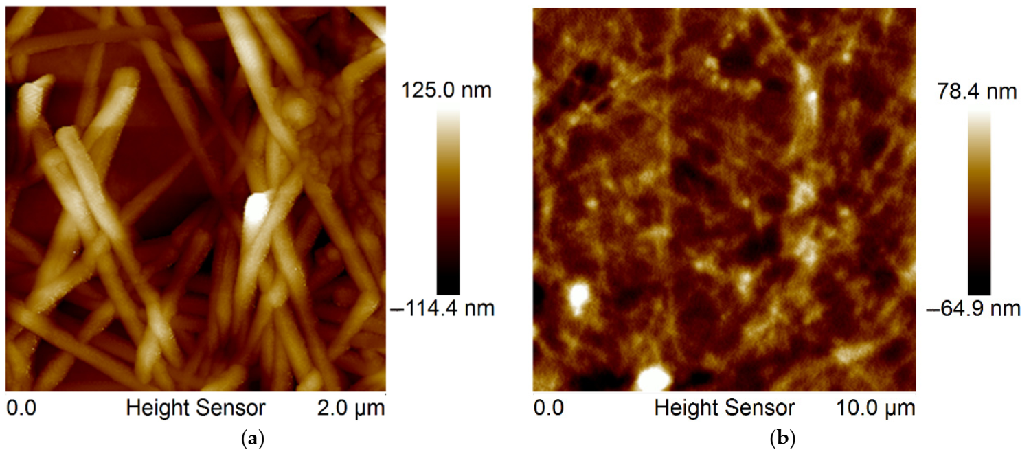
2.3. Preparation of Transparent Composite Electrode Based on AgNWs

In order to reduce the surface roughness of thin films, researchers have put forward several solutions. First, the most direct method is to reduce the diameter of AgNWs and particles as much as possible. Second, the surface roughness of the film is reduced using a pressure-based method. The principle is to use external force to press nanowires into the surface of the flexible plastic substrate, so as to reduce its surface roughness and increase the adhesion between the AgNWs and the substrate. Third, transparent conductive materials are used to fill the gap between nanowires. Although this method can reduce the surface roughness, due to the limited transparency of conductive materials, it will not only reduce the roughness, but also reduce the light transmittance of the film. Fourth, transparent and non-conductive polymers are used for filling.
As a transition metal disulfide, MoS2 is widely used in the fields of electrochemistry [33], energy storage [34], catalysis [35,36,37] and so on. There are many methods to prepare MoS2 thin films, including micromachining [38], chemical vapor deposition [39,40], and liquid ultrasonic [41] and magnetron sputtering [42,43]. In recent years, due to its excellent carrier mobility, MoS2 has been used as hole injection layer in OLED and organic photovoltaic devices.
Unlike graphene, MoS2 is a semiconductor material with a special energy band structure. MoS2 crystal is an indirect band gap semiconductor material with a band gap of about 1.2 eV. The stripped single-layer the MoS2 nano sheet is a direct band gap semiconductor material with a band gap of 1.8 eV or even 1.9 eV. When MoS2 is stripped from bulk materials into MoS2 nanosheets, it shows excellent photoelectric properties and has great potential in electroluminescence and other fields.
In this experiment, the MoS2 target material was purchased from Deyang ONA New Materials Co., Ltd. (Deyang, China) The Purity of the MoS2 target was 99.99%. The magnetron sputtering method was used to sputter a layer of MoS2 on the AgNW transparent conductive film, which effectively inhibited the oxidation of AgNWs in air, and improved the work function of the material while reducing the surface roughness of the film. After that, a layer of PEDOT:PSS film was spin coated on the composite film to fill the gap between AgNWs and further reduce the surface roughness of the film.
Before the experiment, it was necessary to clean the substrate: the PET substrate was cleaned in detergent, acetone solution, isopropanol solution and ethanol solution for 10 min. The MoS2 target was wiped with a dust-free cloth dipped in ethanol solution to remove the surface stains. In the experiment, argon was used as the working gas, and the air intake was set at 45 sccm. We set the pre sputtering time to 3 min, the radio-frequency power to 85 W, the rotation speed to 10 rpm, the target baffle to open state and the sample baffle to closed state. During the sputtering process, the radio-frequency power remained unchanged, the target baffle was set to open state, and the sample baffle was also set to open state.
Before the sputtering started, we needed to pump the vacuum of the chamber to 5 × 10⁻⁴, then fill the chamber with argon, and open the sputtering process when the working pressure was stable at 1.8 Pa. After sputtering, we waited for the temperature to cool to room temperature.
AFM images of the AgNW/MoS2 composite films obtained after 5 min sputtering are shown in Figure 6b. Figure 6a shows the AFM image before sputtering with MoS2. The average roughness of the composite film was 27.6 nm, and the root mean square value relative to the reference plane was 31.5 nm. The average roughness before sputtering was 33.6 nm, which was about 17.8% lower than that before sputtering. At the same time, the maximum roughness of the film was higher than that before sputtering. This was due to the fact that the MoS2 film uniformly covered the surface of the AgNWs, resulting in the increasing of the surface height of the nanowires. From Figure 6b, we can see that the density of the sputtered MoS2 film was good, and no granular impurities were formed on the AgNW film. The MoS2 film completely covered the AgNW film, effectively preventing its oxidation in the air.
PEDOT:PSS is an aqueous solution of high molecular polymer with high conductivity. Depending on the configuration method used, its conductivity will be different. The specific configuration steps of PEDOT:PSS used in this experiment were as follows: Firstly, 2 mL of PEDOT:PSS solution was sucked with a syringe, and the solution was filtered into a vial with a needle filter, so as to filter out the larger particles in PEDOT:PSS solution and not to increase the surface roughness of the film. Then, 120 µL of dimethyl sulfoxide and 4 µL of fluorocarbon surfactant were sucked by a pipette gun and placed in a small bottle containing PEDOT:PSS, and stirred for 4 h with a magnetic stirrer in a sealed environment.
In this experiment, we prepared PEDOT:PSS thin films on AgNWs/MoS2 sputtered for 5 min using the spin coating method. The spin coating equipment comprised a uniform spin coating instrument. Figure 7 shows the AFM images of AgNW transparent conductive film before and after spin coating of the PEDOT:PSS solution. Before spin coating, AgNWs was exposed on the surface of PET. The maximum roughness of the film was 239.4 nm, and the average surface roughness was 27.6 nm. There was a large gap between the nanowires. Figure 7b shows the image after spin coating of PEDOT:PSS solution. It can be seen that AgNWs was completely covered by the PEDOT:PSS solution. At this time, the maximum roughness of the film decreased to 143.3 nm. This was because part of the gap was filled by the solution. The average surface roughness was only 14 nm, which was about 49.3% lower than that before spin coating.

2.4. Fabrication of OLED Device Based on AgNW Composite Electrode

In this experiment, a three-layer structure was adopted. Al was used as a cathode material to emit electrons, LiF was used as an electron injection layer, Alq3 was used as an electron transport layer and a luminescent layer, NPB was used as a hole transport layer, and AgNWs/MoS2/PEDOT:PSS were used as hole injection layers and anodes. The structure of the OLED device is shown in Figure 8a, and the corresponding energy level structure is shown in Figure 8b.
We used the Keithley 2400 digital source meter composite PR655 spectrometer system to test the flexible green OLED device (as shown in Figure 9a). The results show that the light emission of the OLED device prepared by composite film as electrode was relatively uniform, and there was no spot (as was the case for the light emission image), which indicates that the AgNW film prepared by composite film was relatively uniform, and the upper functional layer was not punctured. At the same time, the evaporation rate of the functional layer will also have a great impact on the experimental results. An overly fast evaporation rate will lead to a lack of compactness of the functional layer and increase the likelihood of the occurrence of a spot similar to that of the luminescence image.
In order to detect the stability and service life of the OLED device, we continuously measured the current density of the OLED device at 10 V, as shown in Figure 9b. The test results show that the current density decreased with the increasing of the continuous lighting time, and the rate of decrease was faster in the first two hours. After 6 h, the current density tended to be stable, but the current density was smaller at this time. The service life of the device without packaging was more than 10 h.
Figure 10 shows the voltage current density curve (blue curve) of OLED with the AgNW/MoS2/PEDOT:PSS composite electrode as the anode and the curve (red curve) of OLED with ITO as the anode. We can see that the current density of OLED with the composite electrode as the anode was higher, and the maximum current density was 163.8 mA/cm2 and 48 mA/cm2, respectively. Figure 11 shows the brightness voltage curve of the flexible green OLED device. We can see that the threshold voltage of the OLED device with the composite film as the anode is low, reaching 5 V, while the threshold voltage of the OLED with ITO as the anode was 15 V. This was due to the higher work function of the composite film, which made it easier for the hole to cross the barrier and reach the transport layer. However, the maximum brightness of flexible green OLED was only 1500 cd/m2, while the maximum intensity of OLED prepared by ITO was 2437 cd/m2. The reason may be that the transmittance of the AgNW film was relatively low. At the same time, after the sputtering of the MoS2 film and the spin coating of the PEDOT:PSS film, the transmittance of the AgNW film was affected, which weakened the brightness of the emitted light to a certain extent. At the same time, the existence of AgNWs produced reflection and refraction effects on the light, thereby blocking part of the light.

3. Summary

In this paper, the AgNW TCF with a double-cross arrangement was prepared by mixing the AgNWs in solution using shear force as the driving force. By controlling the deposition density of the nanowires, the roughness, transmittance and conductivity of the double-layer crossed AgNW grid film could be controlled and adjusted. The average transmittance of the double-layer crossed AgNW grid film was 80% in the 400–1000 nm band, when its square resistance was 35 Ω/sq. As an anode, the double-layer crossed AgNW grid film was applied to prepare a flexible green OLED. The threshold voltage of the OLED was only 5 V and the maximum luminance was 1500 cd/m2. A higher work function was found to be able to effectively reduce the starting voltage of the device; thus, it has the potential to prolong the service life of the device and increase the luminous height of the device.

4. Equipment Description in the Paper

The atomic force microscope used in this paper was produced by Bruker company in Karlsruhe, Germany, and the model is the Dimension Edge. The film transmittance meter was produced by Shanghai Guangzhao Company (Shanghai, China), and the model is the GZ502A. The optical microscope was produced by Olympus (Tokyo, Japan), and the model is the BX51M. The UV irradiation equipment was produced by Shenzhen Huiwo Technology Co., Ltd. (Shenzhen, China), and the model is the BZS250GF-TC.

Author Contributions

H.X. wrote the original draft; B.H. and X.J. reviewed and edited the manuscript, L.L. conducted a literature review, P.L. and Q.G. corrected and optimized the manuscript. All authors have read and agreed to the published version of the manuscript.

Funding

The work was supported by the National Natural Science Foundation of China (No. 11775047), and the key scientific research project of the Department of Education of Guangdong Province (2021ZDZX1052, 2021GCZX005, 2021KCXTD040 and 2020KCXTD030).

Institutional Review Board Statement

Not applicable.

Informed Consent Statement

Not applicable.

Data Availability Statement

Data sharing not applicable.

Conflicts of Interest

The authors declare no conflict of interest. The funders contributed to the collection of results and the editing of the manuscript.

References

  1. Wang, Y.; Chen, X.; Zhong, Y.; Loh, K.P. Large area, continuous, few-layered graphene as anodes in organic photovoltaic devices. Appl. Phys. Lett. 2009, 95, 063302. [Google Scholar] [CrossRef]
  2. Kim, B.-J.; Lee, C.; Jung, Y.; Baik, K.H.; Mastro, M.A.; Hite, J.K.; Kim, J. Large-area transparent conductive few-layer graphene electrode in GaN-based ultra-violet light-emitting diodes. Appl. Phys. Lett. 2011, 99, 143101. [Google Scholar] [CrossRef]
  3. Pang, S.; Hernandez, Y.; Feng, X.; Mullen, K. Graphene as transparent electrode material for organic electronics. Adv. Mater. 2011, 23, 2779–2795. [Google Scholar] [CrossRef] [PubMed]
  4. Sa, K.; Mahanandia, P. Conducting reduced graphene oxide film as transparent electrode. Thin Solid Films 2019, 692, 137594. [Google Scholar] [CrossRef]
  5. Lee, B.J.; Yu, H.Y.; Jeong, G.H. Controlled Synthesis of Monolayer Graphene Toward Transparent Flexible Conductive Film Application. Nanoscale Res. Lett. 2010, 5, 1768–1773. [Google Scholar] [CrossRef] [PubMed] [Green Version]
  6. Chang, Y.-M.; Wang, L.; Su, W.-F. Polymer solar cells with poly(3,4-ethylenedioxythiophene) as transparent anode. Org. Electron. 2008, 9, 968–973. [Google Scholar] [CrossRef]
  7. Na, S.-I.; Kim, S.-S.; Jo, J.; Kim, D.-Y. Efficient and Flexible ITO-Free Organic Solar Cells Using Highly Conductive Polymer Anodes. Adv. Mater. 2008, 20, 4061–4067. [Google Scholar] [CrossRef]
  8. Zhou, L.; Yu, M.; Chen, X.; Nie, S.; Lai, W.; Su, W.; Cui, Z.; Huang, W. Screen-Printed Poly(3,4-Ethylenedioxythiophene): Poly(Styrenesulfonate) Grids as ITO-Free Anodes for Flexible Organic Light-Emitting Diodes. Adv. Funct. Mater. 2018, 28, 1705955. [Google Scholar] [CrossRef]
  9. Jiang, S.; Hou, P.-X.; Liu, C.; Cheng, H. High-performance single-wall carbon nanotube transparent conductive films. J. Mater. Sci. Technol. 2019, 35, 2447–2462. [Google Scholar] [CrossRef]
  10. Alshammari, A.S.; Sam, F.L.M.; Rozanski, L.J.; Mills, C.A.; Beliatis, M.J.; Jayawardena, K.D.G.I.; Underwood, J.M.; Silva, S. Controlled growth and spray deposition of silver nanowires for ITO-free, flexible, and high brightness OLEDs. Phys. Status Solidi A-Appl. Mater. Sci. 2017, 214, 1600561. [Google Scholar] [CrossRef]
  11. Lian, L.; Wang, H.; Dong, D.; He, G. Highly robust and ultrasmooth copper nanowire electrode by one-step coating for organic light-emitting diodes. J. Mater. Chem. C 2018, 6, 9158–9165. [Google Scholar] [CrossRef]
  12. Tseng, J.-Y.; Lee, L.; Huang, Y.-C.; Chang, J.-H.; Su, T.-Y. Pressure Welding of Silver Nanowires Networks at Room Temperature as Transparent Electrodes for Efficient Organic Light-Emitting Diodes. Small 2018, 14, 1800541. [Google Scholar] [CrossRef]
  13. Wang, Y.; Liu, P.; Wang, H.; Zeng, B.; Wang, J. Flexible organic light-emitting devices with copper nanowire composite transparent conductive electrode. J. Mater. Sci. 2018, 54, 2343–2350. [Google Scholar] [CrossRef]
  14. Park, K.; Woo, K.; Kim, J.; Lee, D.; Ahn, Y.; Song, D.; Kim, H.; Oh, D.; Kwon, S.; Lee, Y. High-Resolution and Large-Area Patterning of Highly Conductive Silver Nanowire Electrodes by Reverse Offset Printing and Intense Pulsed Light Irradiation. ACS Appl. Mater. Interfaces 2019, 11, 14882–14891. [Google Scholar] [CrossRef]
  15. Hecht, D.S.; Hu, L.; Irvin, G. Emerging Transparent Electrodes Based on Thin Films of Carbon Nanotubes, Graphene, and Metallic Nanostructures. Adv. Mater. 2011, 23, 1482–1513. [Google Scholar] [CrossRef]
  16. Layani, M.; Kamyshny, A.; Magdassi, S. Transparent conductors composed of nanomaterials. Nanoscale 2014, 6, 5581–5591. [Google Scholar] [CrossRef]
  17. Lee, J.-Y.; Connor, S.T.; Cui, Y.; Peumans, P. Solution-processed metal nanowire mesh transparent electrodes. Nano Lett. 2008, 8, 689–692. [Google Scholar] [CrossRef]
  18. Lee, J.-Y.; Connor, S.T.; Cui, Y.; Peumans, P. Semitransparent Organic Photovoltaic Cells with Laminated Top Electrode. Nano Lett. 2010, 10, 1276–1279. [Google Scholar] [CrossRef]
  19. De, S.; Higgins, T.M.; Lyons, P.E.; Doherty, E.M.; Nirmalraj, P.N.; Blau, W.J.; Boland, J.J.; Coleman, J.N. Silver Nanowire Networks as Flexible, Transparent, Conducting Films: Extremely High DC to Optical Conductivity Ratios. Acs Nano 2009, 3, 1767–1774. [Google Scholar] [CrossRef]
  20. Hu, L.; Kim, H.S.; Lee, J.-Y.; Peumans, P.; Cui, Y. Scalable Coating and Properties of Transparent, Flexible, Silver Nanowire Electrodes. ACS Nano 2010, 4, 2955–2963. [Google Scholar] [CrossRef]
  21. Guo, X.; Guo, C.W.; Wang, C.; Li, C.; Sun, X. AlGaInP LED with low-speed spin-coating silver nanowires as transparent conductive layer. Nanoscale Res. Lett. 2014, 9, 670. [Google Scholar] [CrossRef] [Green Version]
  22. Lagrange, M.; Langley, D.P.; Giusti, G.; Jimenez, C.; Brechet, Y.; Bellet, D. Optimization of silver nanowire-based transparent electrodes: Effects of density, size and thermal annealing. Nanoscale 2015, 7, 17410–17423. [Google Scholar] [CrossRef]
  23. Duan, X.F.; Huang, Y.; Cui, Y.; Wang, J.; Lieber, C. Indium phosphide nanowires as building blocks for nanoscale electronic and optoelectronic devices. Nature 2001, 409, 66–69. [Google Scholar] [CrossRef]
  24. Myung, S.; Lee, M.; Kim, G.T.; Ha, J.S.; Hong, S. Large-Scale “Surface-Programmed Assembly” of Pristine Vanadium Oxide Nanowire-Based Devices. Adv. Mater. 2005, 17, 2361–2364. [Google Scholar] [CrossRef]
  25. Heo, K.; Cho, E.; Yang, J.-E.; Kim, M.-H.; Lee, M.; Lee, B.-Y.; Kwon, S.-G.; Lee, M.-S.; Jo, M.-H.; Choi, H.-J. Large-Scale Assembly of Silicon Nanowire Network-Based Devices Using Conventional Microfabrication Facilities. Nano Lett. 2008, 8, 4523–4527. [Google Scholar] [CrossRef]
  26. Wang, M.C.P.; Gates, B.D. Directed assembly of nanowires. Mater. Today 2009, 12, 34–43. [Google Scholar] [CrossRef]
  27. Hassan, M.; Zhan, H.-J.; Wang, J.-L.; Liu, J.; Chen, J. Self-Assembly Anisotropic Magnetic Nanowire Films Induced by External Magnetic Field. ChemistryOpen 2020, 9, 588–592. [Google Scholar] [CrossRef]
  28. Duan, X.F.; Niu, C.M.; Sahi, V.; Chen, J.; Parce, J.; Empedocles, S.; Goldman, J. High-performance thin-film transistors using semiconductor nanowires and nanoribbons. Nature 2003, 425, 274–278. [Google Scholar] [CrossRef]
  29. Huang, Y.; Duan, X.F.; Wei, Q.Q.; Lieber, C.-M. Directed assembly of one-dimensional nanostructures into functional networks. Science 2001, 291, 630–633. [Google Scholar] [CrossRef] [Green Version]
  30. Yu, G.; Cao, A.; Lieber, C.M. Large-area blown bubble films of aligned nanowires and carbon nanotubes. Nat. Nanotechnol. 2007, 2, 372–377. [Google Scholar] [CrossRef]
  31. Qi, X.; Lu, Z.; You, E.M.; He, Y.; Zhang, Q.; Yi, H.; Li, D.; Ding, S.; Jiang, Y.; Xiong, X. Nanocombing Effect Leads to Nanowire-Based, in-Plane, Uniaxial Thin Films. ACS Nano 2018, 12, 12701–12712. [Google Scholar] [CrossRef] [PubMed]
  32. Noy, A.; Frisbie, C.D.; Rozsnyai, L.F.; Wrighton, M.S.; Lieber, C. Chemical Force Microscopy—Exploiting Chemically-Modified Tips to Quantify Adhesion, Friction, and Functional-Group Distributions in Molecular Assemblies. J. Am. Chem. Soc. 1995, 117, 7943–7951. [Google Scholar] [CrossRef]
  33. Cheng, S.; Xia, X.; Liu, H.; Chen, Y. Core-shell structured MoS2 @S spherical cathode with improved electrochemical performance for lithium-sulfur batteries. J. Mater. Sci. Technol. 2018, 34, 1912–1918. [Google Scholar] [CrossRef]
  34. Chen, Y.M.; Yu, X.Y.; Li, Z.; Paik, U.; Lou, X.W. Hierarchical MoS2 tubular structures internally wired by carbon nanotubes as a highly stable anode material for lithium-ion batteries. Sci. Adv. 2016, 2, e1600021. [Google Scholar] [CrossRef] [Green Version]
  35. Hao, X.; Jin, Z.; Yang, H.; Lu, G.; Bi, Y. Peculiar synergetic effect of MoS2 quantum dots and graphene on Metal-Organic Frameworks for photocatalytic hydrogen evolution. Appl. Catal. B-Environ. 2017, 210, 45–56. [Google Scholar] [CrossRef]
  36. Yang, Y.; Zhang, K.; Ling, H.; Li, X.; Chan, H.; Yang, L.; Gao, Q. MoS2-Ni3S2 Heteronanorods as Efficient and Stable Bifunctional Electrocatalysts for Overall Water Splitting. Acs Catal. 2017, 7, 2357–2366. [Google Scholar] [CrossRef]
  37. Peng, K.; Fu, L.; Yang, H.; Ouyang, J.; Tang, A. Hierarchical MoS2 intercalated clay hybrid nanosheets with enhanced catalytic activity. Nano Res. 2017, 10, 570–583. [Google Scholar] [CrossRef]
  38. Splendiani, A.; Sun, L.; Zhang, Y.; Li, T.; Kim, J. Emerging Photoluminescence in Monolayer MoS2. Nano Lett. 2010, 10, 1271–1275. [Google Scholar] [CrossRef]
  39. Lee, Y.-H.; Zhang, X.-Q.; Zhang, W.; Chang, M.; Lin, C.; Chang, K.; Yu, Y.; Wang, J.; Chang, C.; Li, L.; et al. Synthesis of Large-Area MoS2 Atomic Layers with Chemical Vapor Deposition. Adv. Mater. 2012, 24, 2320–2325. [Google Scholar] [CrossRef] [Green Version]
  40. Shi, Y.; Zhou, W.; Lu, A.-Y.; Fang, W.; Lee, Y.; Hsu, A.-L.; Kim, S.-M.; Kim, K.-K.; Yang, H.-Y.; Li, L.-J.; et al. van der Waals Epitaxy of MoS2 Layers Using Graphene As Growth Templates. Nano Lett. 2012, 12, 2784–2791. [Google Scholar] [CrossRef]
  41. Nicolosi, V.; Chhowalla, M.; Kanatzidis, M.G.; Strano, M.S.; Coleman, J.N. Liquid Exfoliation of Layered Materials. Science 2013, 340, 1420. [Google Scholar] [CrossRef] [Green Version]
  42. Gong, C.; Xiao, J.; Zhu, L.; Wang, Z.; Ma, S. Effect of Deposition Pressure on the Microstructure and Optical Band Gap of Molybdenum Disulfide Films Prepared by Magnetron Sputtering. Coatings 2019, 9, 570. [Google Scholar] [CrossRef] [Green Version]
  43. Zhou, P.; Li, W.; Jin, X. Electrochemical Hydrogen Permeation Properties of MoS2 and Ni80Cr20 Films Prepared by Magnetron Sputtering on Pure Iron. J. Electrochem. Soc. 2018, 165, E256–E261. [Google Scholar] [CrossRef]
Figure 1. Contact angle test diagram: (a) PET without UV irradiation; (b) PET after UV irradiation for 15 min.
Coatings 12 00026 g001
Figure 2. (a) Schematic diagram of mixing assisted AgNW assembly—the beaker diameter was 5 cm and the rotating speed was 400 r/min. (b) Optical microscope images of uniaxial AgNW films.
Coatings 12 00026 g002
Figure 3. Optical microscope images of single layer and uniaxially aligned AgNW films after amination: (a) after ultraviolet irradiation; (b) without UV irradiation. (c) Optical microscope images of double-cross AgNW transparent conductive film.,arrows indicate the nanowire alignment direction.
Coatings 12 00026 g003
Figure 4. Transmittance of AgNW film.
Coatings 12 00026 g004
Figure 5. AFM images of double-layered AgNW film: (a) 3D image; (b) film step diagram.
Coatings 12 00026 g005
Figure 6. AFM images of AgNW films: (a) before sputtering with MoS2; (b) after sputtering with MoS2.
Coatings 12 00026 g006
Figure 7. AFM image of AgNW conductive film: (a) before spin coating; (b) after spin coating.
Coatings 12 00026 g007
Figure 8. Schematic diagram of OLED device structure and energy level: (a) structure diagram; (b) energy level diagram.
Coatings 12 00026 g008
Figure 9. The real picture of flexible green OLED and its stability measurement results: (a) the real picture of light emission; (b) time–current density curve.
Coatings 12 00026 g009
Figure 10. Voltage current density curve of OLED device. The upper left figure shows the circle marking area.
Coatings 12 00026 g010
Figure 11. Voltage brightness curve of OLED device.
Coatings 12 00026 g011
Publisher’s Note: MDPI stays neutral with regard to jurisdictional claims in published maps and institutional affiliations.

