Review

Role of Crystallographic Orientation of β-Sn Grain on Electromigration Failures in Lead-Free Solder Joint: An Overview

1
Department of Mechanical Engineering, College of Electrical and Mechanical Engineering, National University of Sciences and Technology, Islamabad 46060, Pakistan
2
Department of Chemistry, School of Natural Sciences, National University of Sciences and Technology, H-12, Islamabad 44000, Pakistan
3
School of Mechanical & Manufacturing Engineering, National University of Sciences and Technology (NUST), Islamabad 44000, Pakistan
4
Higher Education Institution Centre of Excellence (HICoE), UM Power Energy Dedicated Advanced Centre (UMPEDAC), Level 4, Wisma R&D, Universiti Malaya, Jalan Pantai Baharu, Kuala Lumpur 59990, Malaysia
5
Centre of Advanced Materials, Department of Mechanical Engineering, Faculty of Engineering, Universiti Malaya, Kuala Lumpur 50603, Malaysia
6
Department of Mechanical Engineering, College of Engineering, Umm Al-Qura University, Makkah City 24382, Saudi Arabia
7
Center of Research, Faculty of Engineering, Future University in Egypt, New Cairo 11835, Egypt
8
Department of Civil Engineering, College of Engineering, King Khalid University, Abha 61421, Asir, Saudi Arabia
*
Author to whom correspondence should be addressed.
Coatings 2022, 12(11), 1752; https://doi.org/10.3390/coatings12111752
Submission received: 29 September 2022 / Revised: 2 November 2022 / Accepted: 7 November 2022 / Published: 15 November 2022

Abstract

:
Due to the miniaturization of electronic devices, electromigration became one of the serious reliability issues in lead-free solder joints. The orientation of the β-Sn grain plays an important role in electromigration failures. Several studies have been carried out to investigate the effect of Sn grain orientation on electromigration. The efforts involve the influence of β-Sn grain orientation on the migration of Cu, Sn, and Ni atoms, on the morphology of the solder joint, and on the formation of Cu6Sn5 and (Cu, Ni)6Sn6 in the lead-free solder joint during electromigration. The current review provides a detailed review of past studies which were conducted to investigate the influence of β-Sn grain orientation on electromigration failures in lead-free solder joints.

1. Introduction

In chip technology, lead-based solder alloys no longer receive any interest in research. Scientists are eliminating lead-based solders to avoid the inherent toxicity of lead in electronic industries. As a result of lead banning due to its environmental issues, lead-free solders have become a standard material for electronic joints [1,2,3]. To replace lead-based solders, researchers used various metals (Au, Ag, Cu, Bi, In, Zn) and developed a number of lead-free solder alloys [4,5,6,7,8]. These solder alloys have different melting temperatures and different properties.
The replacement of lead-based solder joints should have at least equal or better material properties such as mechanical, electrical, thermal, and structural properties than a SnPb solder. Because of its good reaction ability with many metals, the formation of intermetallic compound and low temperature soldering, researchers suggested that a Sn-based solder is one of the good replacement options of the SnPb solder joint [9,10,11,12].
In the past, the United Nations Environment Program suggested that germanium (Ge) is also dangerous for human health. It is one of the good reactive elements and normally a trace amount of germanium is added to the Sn due to its high cost. Zinc shows dross due to the formation of oxides during the soldering, and it also has poor wetting properties. Indium has good wettability and good effects on physical properties of the solder alloys. However, the cost of indium is high compared to other solder alloys. Bi also has excellent wettability and physical properties; however, since Bi production is linked to lead, the use of Bi is also limited.
Hence, by comparing the advantages and disadvantages of Sn-based solder alloys, it is found that the long list of Sn-based solder joints becomes a short list of promising replacement candidates such as Sn-3.5Ag, Sn-3.5Ag-0.7Cu, Sn-0.7Cu, and Sn-3.5Ag-4.8Bi. Consequently, Sn-Ag-Cu, eutectic Sn-Cu, and Sn-Ag were recommended as promising replacements of the lead-based solder alloys by the National Electronics Manufacturing Initiative. Researchers found that an SAC solder has better tensile strength, good creep and fatigue properties. To complement these properties, it is important to improve structural and electrical properties. Electromigration (EM) is one of the serious factors which influences the electrical and structural properties. So, it is important to suppress EM failures in the solder joints.
Electromigration (EM) is a mass transportation phenomenon driven by high-current density, and it is also known as the diffusion of atoms, which are driven by high-current density [13]. When a heavy electron wind passes from the substrate to the solder joint, it collides and drifts with the Cu atoms present at the cathode interface of the solder joint. Current wind transfers the momentum to the Cu atoms present at the cathode interface of the solder joint due to which the Cu atoms migrate from the cathode side toward the anode side [14,15,16,17]. The migration of Cu atoms forms vacancies at the cathode side which evolve into voids formation after a long period of EM [18,19]. In the flip-chip solder joint, the current enters from the corner of the solder joint (Figure 1). At the corner of the solder bump, the uneven distribution of heavy current wind takes place, due to which current crowding effect occurs in the solder joint [20]. The non-uniformity of current wind at the corner of the solder also promotes a Joule heating effect. Joule heating and current crowding effects increase the electromigration process in the solder joint [21,22]. EM usually influences the migration of Cu atoms from the cathode to the anode side of the solder joint. This leads to reliability concerns for the solder joint [23,24,25]. Electromigration issues involve the formation of voids, cracks, and damage at the cathode side, the reduction in thickness of the interfacial Intermetallic Compound (IMC) layer at the cathode side, and the rapid growth of the interfacial IMC layer at the anode side [26].
Due to the Joule heating effects present in the solder joint, rapid diffusion of Cu atoms will take place. Rapid Cu diffusion creates vacancies at the cathode side of the solder joint which leads to the formation of voids and cracks and finally the separation of the joint from the cathode interfaces [27,28,29]. These voids and cracks reduce the conduction path of the electric current. Non-uniformity of the current increases the current’s density in certain areas [29,30]. By increasing the EM time, the Cu diffusion will also be increased. In the tin-silver-copper (Sn-3.0Ag-0.5Cu or SAC305) solder joints, in past studies, a substantial increase in the IMC thickness at the anode side was observed with a corresponding decrease at the cathode side by increasing the duration of the EM test [31]. Longer EM time provides more Cu migration from the cathode side to the anode side. Migrated Cu atoms form a thicker layer of IMCs, such as Cu6Sn5, at the anode side by reacting with Sn atoms. As IMCs have brittle properties, if the IMC layer at the anode side becomes thicker then it will reduce the mechanical strength of the solder joint [31]. On the other hand, directional migration of Cu atoms towards the anode rapidly decreases the IMC layer at the cathode interfaces, which finally leads to the separation of the solder joint from the cathode interface [32,33].
The formation of voids at the cathode side and the formation of a thicker layer of IMC at the anodic side degrade the structural properties of the solder bump. The structural degradation of the cathode and anodic interfaces can cause serious issues on the mechanical performance of the solder joint [32,33]. Past studies found that a longer EM time decreased the shear strength of the SAC305 solder, and the fracture will be shifted from the solder bulk to the cathodic interface with a brittle behavior [32]. Zhang et al. also found similar results [33].
A solder bump has much lower thermal conductivity than a trace [35]. The actual temperature of the solder bump can thus be significantly higher than the ambient temperature of the solder bump. Due to the nature and construction of the solder bump, the bump temperature is governed by the heat dissipation of the chip and the Joule heating effect [35]. Since Joule heating is a nonlinear function of the current (I), any increase in a current adversely affects the solder bump temperature [35,36]. It is essential to control the temperature of the solder bump to reduce the failure in the solder bump. Different elements in the solder bump can be resistive leading to an increase in overall bump resistance. This might affect the Joule heating characteristics in the solder bump. In the past, the sizes of the solder joint and traces were larger. So, the occurrence of heating was very low due to a bigger size. The Joule heating effects were not so pronounced in the solder joints and traces. As of recently, the size of the solder joint and traces have been diminished. The scaling down in the size of the solder joint and traces has impacted not only the solder joints but also the traces that form the interconnection. Each of the new generations of flip-chip devices has had to deal with higher Joule heating in a trace and smaller-sized solder joints. The Joule heating effect is not only because of size reduction of the solder joint and traces but also because of an increase in current density [37,38,39]. The high temperature in the solder joint will speed up the electromigration process in the solder joint. So, it is very important to minimize the formation of Joule heating at the solder joint and traces to minimize the EM failures.
When heavy current density enters into the solder from the substrate, it changes the direction from horizontal to vertical [40] as shown in (Figure 2). During current flow, most of the current enters from the corner of the solder bump. The distribution of the electric current becomes non-uniform at the cathode interface [41]. The non-uniformity in the distribution of current density creates current crowding at the cathodic interface [41]. The explanation of current crowding is also given in (Figure 2). The non-uniform distribution of current density significantly increases the current density at the corner, which increases the current crowding. An effort was made to investigate and to understand the current crowding effect on the solder joint in the presence of high-current density [42]. A 3D simulation model was constructed to understand the effect of current crowding. Electromigration tests were run for different time intervals. Figure 2a–h show X-ray micrographs of the samples. It was found that a high amount of current enters from the corner of the solder joint in all samples. FEA simulation detected that, at the corner of the solder joint, the current density significantly increases from 1.1 × 10⁴ A/cm2 to 3.58 × 10⁴ A/cm2 at the corner of the solder joint (Figure 2g).
Other than the Joule heating effect [43] and current crowding effects [44], the grain orientation of β-Sn was also found to be one of the root causes of electromigration failures. In the last decade, several experimental studies have been carried out on the influence of β-Sn grain orientation on electromigration failures. Those studies involve the influence of β-Sn grain orientation on the migration of Cu, Sn, and Ni atoms, on the morphology of the solder joint, and on the formation of Cu6Sn5 and (Cu, Ni)6Sn6 in the lead-free solder joint during electromigration. The current review covers details of past studies that were carried out to investigate the influence of β-Sn grain orientation on electromigration failures.

2. Influence of Crystallographic Orientation of β-Sn Grain on EM

The orientation of β-Sn grain plays a vital role in the Cu diffusion from the cathodic to the anodic interface of the solder joint. β-Sn grain possesses a tetragonal cell, and it is found that when the c-axis of β-Sn grain is in the same direction of the current flow, the Cu diffusion will be faster [45]. The vertical direction of the c-axis of the current flow has been found as an ideal condition to reduce the diffusion of Cu atoms [41,46]. In early studies [47], it was also found that the diffusion coefficient of Cu atoms in the a-axis and b-axis of the β-Sn grain is 500 times slower than the c-axis. Hence, the orientation of the c-axis causes serious issues and facilitates the excessive migration of Cu atoms.
Researchers found that, during the electromigration process, the orientation of β-Sn grain could be responsible for the structural degradation of solder joints such as a serrated dissolution at the cathode side, a reduction in the IMC thickness at the cathode side, an increase in the IMC thickness at the anodic interface, and a formation of voids at the cathodic interface. The influence of Sn grain orientation on structural degradation of the solder joint is discussed below.
Past studies investigated the influence of β-Sn grain orientation on the migration of Cu atoms. The migration of Cu atoms was found to be fast when the direction of the current and the direction of the c-axis are in the same direction (Figure 3), and more EM effects were observed (Figure 3c). The migration of the Cu atom was significantly controlled when the angle between the c-axis and the current flow direction was bigger (Figure 3b), and reductions in the EM were observed. The angle θ between the c-axis of the Sn grain and the direction of the current flow plays a very important role in Cu migration from the cathode side to the anode side of the solder joint [41]. The θ angle is an angle between the c-axis of the β-Sn grain and the direction of the current flow. It was observed that high θ angle reduces the Cu migration and lower θ angle facilitates the Cu atoms migration which results in EM failures.
To clarify the effect of θ angle on Cu migration, a solder joint containing only two grains were prepared and an EM test was conducted [48]. The study was conducted for two samples containing a low θ angle and a high θ angle (Figure 4). In the first sample, the direction of the current was from the low to the high θ angle. It was found that in the low θ angle, the Cu diffusion was very fast. It produced voids at the cathode side of the solder joint [48]. The grain with a high θ angle showed very less Cu diffusion towards the anode side (Figure 5). Due to different grain orientations, a thick IMC layer was produced between both of the grains. In the second sample, the direction of the current was from the high to the low θ angle. Significant reduction in the Cu diffusion was found due to the high θ angle (Figure 6). By comparing Figure 5 and Figure 6, it can be seen that in different β-Sn grain orientations, the EM influenced differently. The c-axis of the β-Sn grain facilitated the migration of the Cu atom from the cathode to the anode side, while other axes of the β-Sn grain suppressed the Cu migration. In both figures, a huge Cu migration along the c-axis caused voids at the anode and a thick layer at the cathode side.

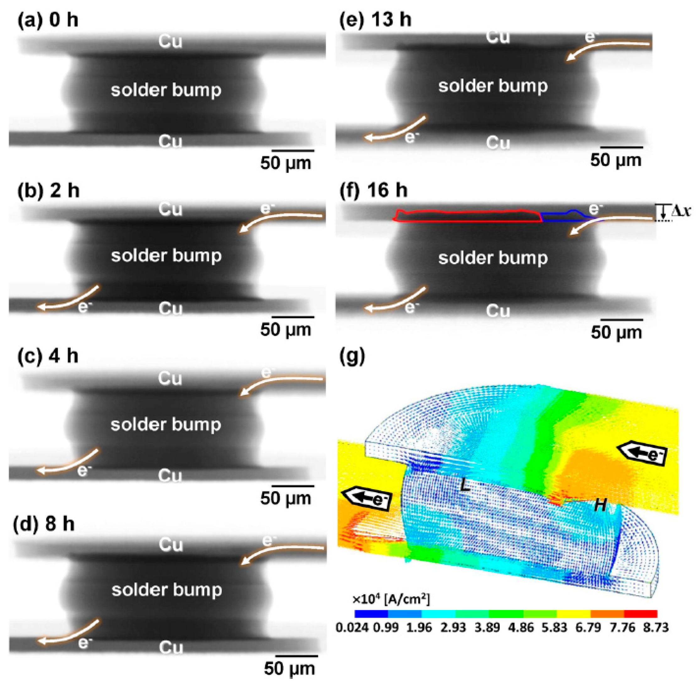
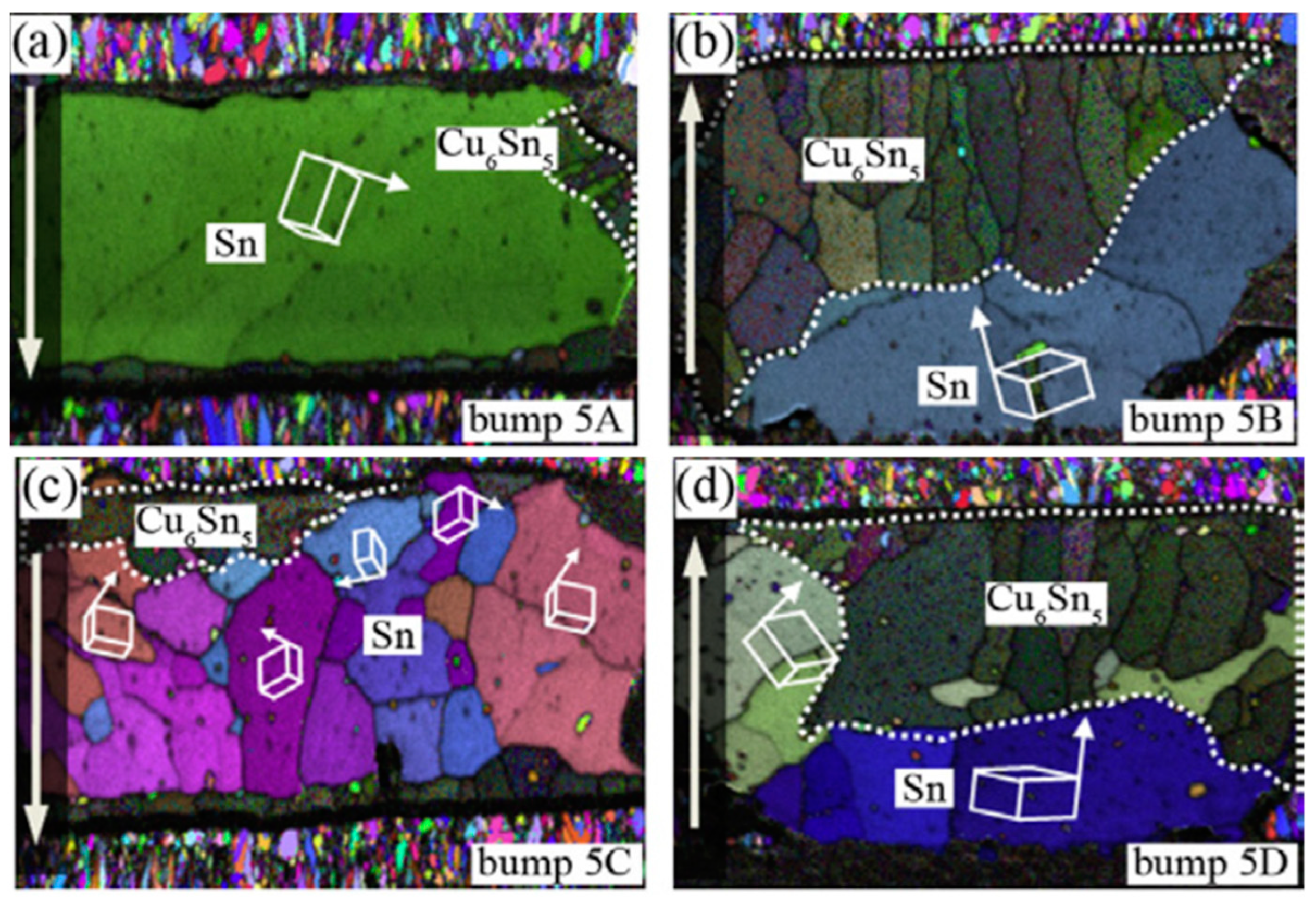
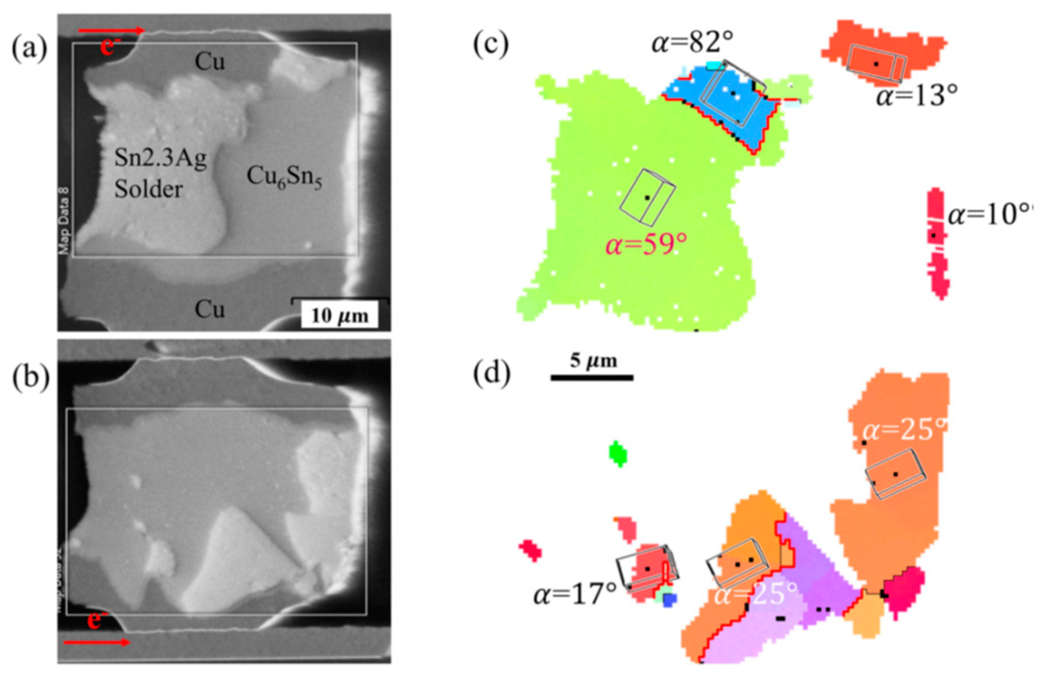
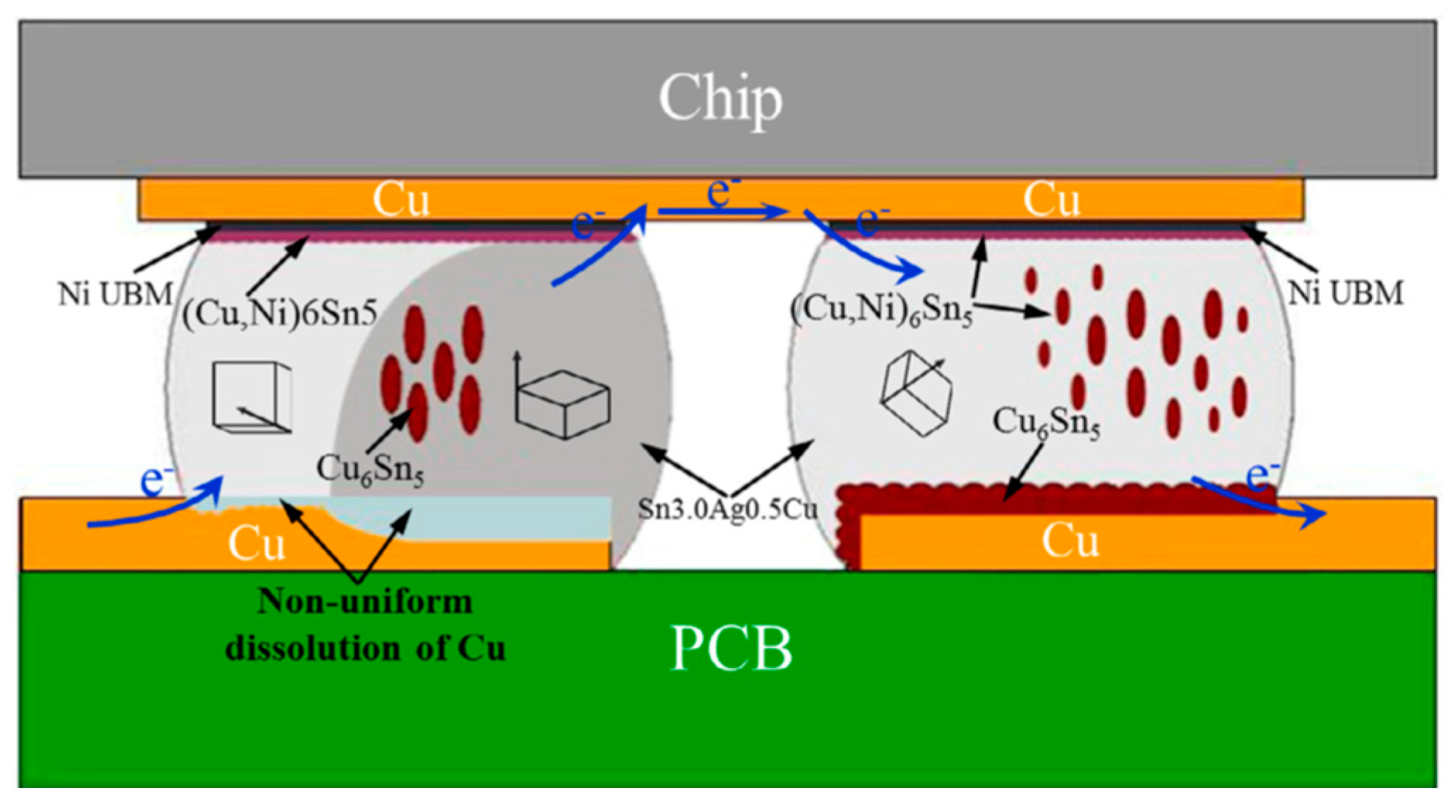
2.1. Influence on Cu Migration

In previous studies, it was also found that the rate of diffusivity of Cu atoms is different along a different axis of the β-Sn grain [48]. Yang et al. quantified the diffusivity of Cu atoms into Sn along the a-axis and c-axis of the β-Sn grain into the Sn2.6Ag solder joint [41]. The EM test was conducted on 4 different samples. It was found that in each sample, the orientation was different and in each different orientation the EM behavior was different. Based on orientation, they quantified the diffusivity ratio of Cu by using the following method [41].
J E M C u = C C u D C u S n k t z C u S n * e ρ S n j
where C C u is the local molar concentration of Cu in Sn, D C u S n is the diffusion coefficient of Cu in Sn, z C u S n * is the effective charge number of Cu in Sn, k is the Boltzmann constant, t is the absolute temperature, e is a charge of an electron, ρ S n is the resistivity of Sn, and j is the applied electron current density.
The term D C u S n for the a-axis and the c-axis was calculated as below [41,49].
D C u a a x i s = 2.4 × 10 3 exp 33.18 k J / m o l e k T c m 2 / s
D C u c a x i s = 1.0 × 10 3 exp 16.8 k J / m o l e k T c m 2 / s
The ratio of Cu diffusivity on the a-axis and c-axis of Sn at different temperatures is given in Figure 7. It can be seen in the figure that the ratio of Cu diffusivity decreased by increasing the temperature. The authors found that at 150 °C the diffusivity was approximately 44. However, at a 50 °C temperature, it significantly increased to 185.
Another study was also carried out to investigate the Cu diffusivity in β-Sn [50]. The author quantified the Cu diffusion by a mathematical model as well as by experimental data. Their findings also concluded that the Cu diffusion is much faster at the c-axis of the β-Sn grain. Other researchers also found similar results [51,52]. Refs [49,53,54] quantified the diffusivity of Cu, Ag, Ni, and Sn into β-Sn. Their findings revealed that Cu, Ag, Ni, and Sn atoms showed low diffusivity through the a-axis, while faster at the c-axis of the β-Sn grain. The values of diffusivity of Cu, Ag, Ni, and Sn into β-Sn are given in Table 1.
Hence, it can be said that the orientation of Sn grain plays a very important role during the electromigration process. The fine-grain structure can suppress the electromigration failures in the Sn-based solder joints.

2.2. Influence on the Microstructure of the Solder Bump

The orientation of the β-Sn grain plays a very important role in microstructural changes of solder joints during the electromigration process. At a low θ angle, rapid Cu migration takes place. The migration of the Cu will form voids and accelerate the serrated dissolution at cathode interfaces. Cu migration also forms a thicker layer of the IMC at the anode side of the solder joint. The detail of these structural changes has been discussed below.

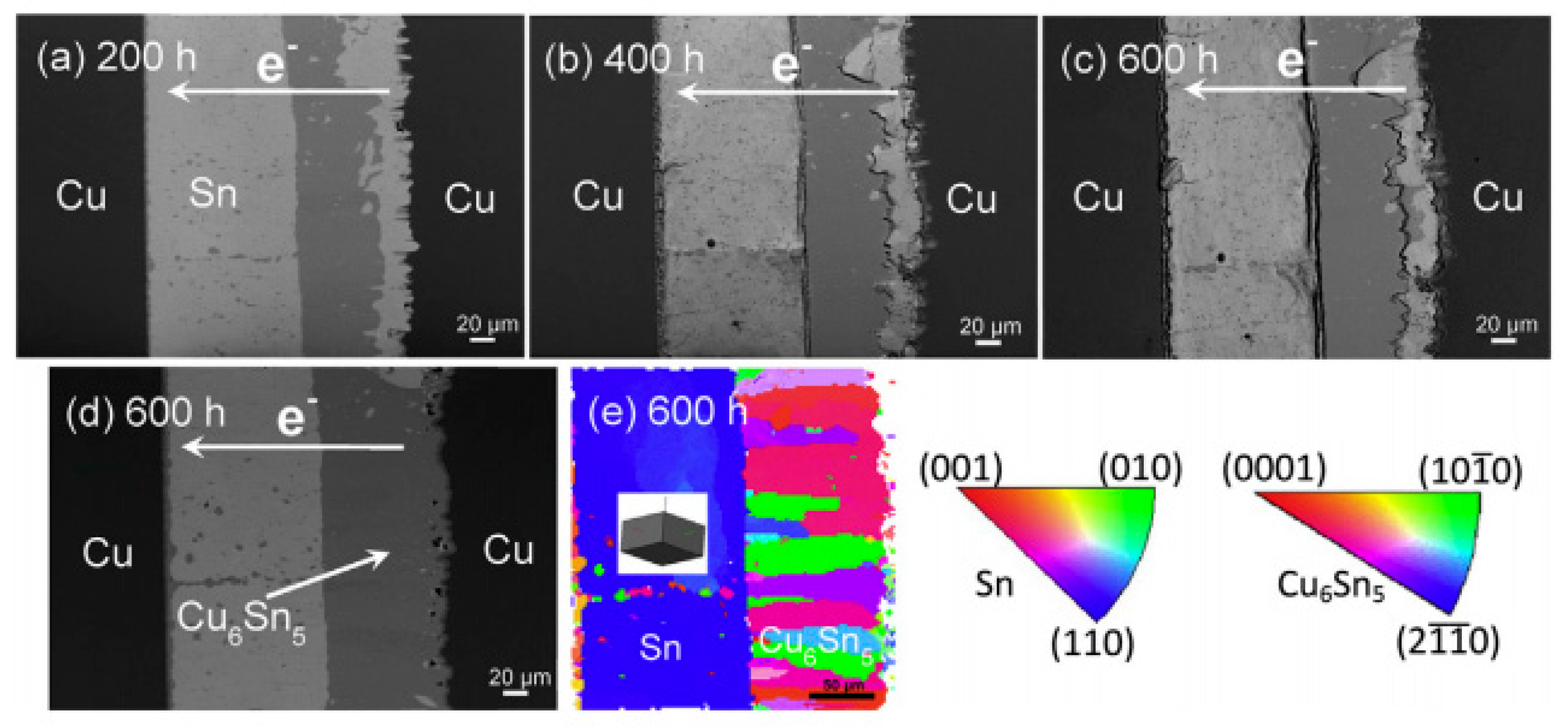
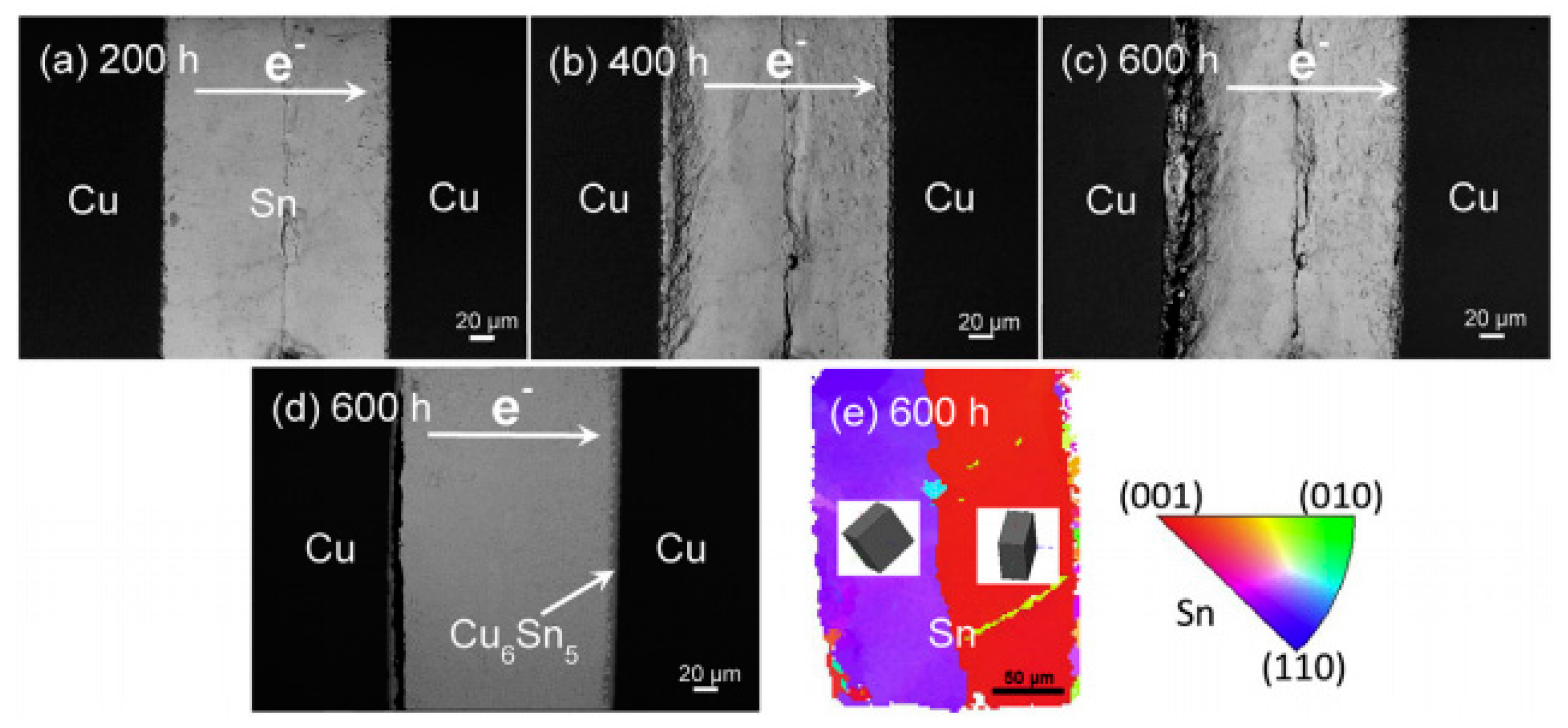
2.2.1. Serrated Dissolution at the Cathode Interface

Chen et al. reported the effect of the orientation of the β-Sn grain on the structural changes of solder joints [55]. It was observed that the θ angle plays a vital role during the EM test. A lower θ angle accelerates the Cu migration from the cathodic to the anodic interface. Rapid migration of Cu atoms formed serrated edges at the cathode, and a thicker layer of the interfacial IMC at the anode side. Yang et al. also found similar results during their experiments [41]. They found a migration of Cu in high θ angles as well as low θ angles of the β-Sn grain at the cathode interface of the solder joint. They also found serrations where the θ angle was smaller. A smaller θ angle facilitated and accelerated the migration of Cu atoms. For other places of the cathode interfaces where the θ angle was higher, the migration of Cu was slower, and serration did not take place Figure 8.

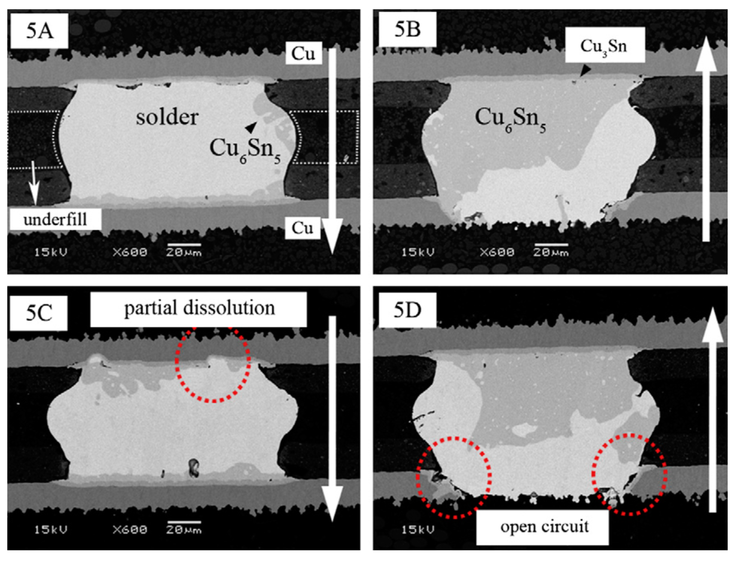
2.2.2. Voids and Cracks at the Cathode Side

Huang et al. found that a low θ between the electron flow and the c-axis of β-Sn grain caused the formation of voids and the propagation of cracks at the cathode interface of the solder joint [48]. Lee et al. also found similar findings in their studies [46] Figure 9. In their studies, it was found that the favorable direction of the c-axis of the β-Sn grain facilitates the Cu migration at the cathode, and a massive Cu migration took place. Due to this, the formation of voids and the propagation of cracks occurred, and samples failed to conduct an electric current from the cathode interface. The formation of voids and cracks are given in Figure 9 (5D). The Sn inverse pole orientation map of the Figure (Figure 9 5A–D) is given in Figure 10a–d. It can be seen clearly from the SEM images in Figure 9 (5D) and the orientation map in Figure 10d that when the c-axis of β-Sn grain was parallel or formed a small θ angle with the electron flow, a massive Cu migration occurred. Due to the massive Cu migration, voids and cracks were formed at the cathodic interface Figure 9 (5D). On the other side, where the c-axis of the β-Sn grain was perpendicular or formed a high θ angle with the electron wind, the migration of Cu was much slower, and the formation of voids and cracks was suppressed (Figure 9 5A,C). The Sn inverse pole orientation map of Figure 9 5A,C is given in Figure 10a,c.

2.2.3. Influence on the Growth of Cu6Sn5 IMC

The studies of Lee et al. [46] revealed that the formation of Cu6Sn5 in the solder joint also depends on the orientation of the β-Sn grain. They found that the formation of Cu6Sn5 IMC was faster at a low θ angle and slower at a higher θ angle. A low θ angle formed a thicker layer of IMC at the anode side of the sample (Figure 9 and Figure 10).
Shen et al. also performed an investigation on the formation of Cu6Sn5 in a different orientation of the β-Sn grain [56]. The study was carried out on Cu/Sn-2.3Ag/Cu micro bumps under a current density of 4 × 10⁴ A/cm2, and the applied temperature was 165 °C. An electromigration test was run for 65 h. The test was run for 40 micro bumps. Their results revealed that one micro bump contains several β-Sn grains. All grains had different θ angles. The formation of Cu6Sn5 was different at different angles. It was found that in an area where the θ angle was smaller, more Cu migration occurred and a thick layer of Cu6Sn5 was formed at the anode side. In the area where the θ angle was high, less Cu migration was found which formed a thin layer of Cu6Sn5 IMC at the anode on the side of micro bumps. The formation of Cu6Sn5 in different angles of the c-axis with electron flow is given in Figure 11 and Figure 12. Similar findings were also found by other researchers in the past [46,57,58,59]

2.3. Influence on Ni migration

Researchers also carried out studies to investigate the influence of the β-Sn grain orientation on the diffusion of Ni atoms from the cathode to the anode sides of the solder joint [45,60,61,62]. Their results revealed that the diffusion of Ni in the β-Sn grain was extremely slower than Cu. They also found that the diffusivity of Ni was different at the different axes of the β-Sn grain. The values of diffusivity of Ni, Cu, Ag, and Sn into the β-Sn matrix are given in Table 1.
Huang et al. investigated the influence of Sn grain orientation on Ni diffusion [60]. The test was conducted on an SAC 305 flip-chip solder joint. The solder joint contained Ni under bump metallization (UBM) on the chip side while the PCB side contained Cu. The electromigration test was conducted for a maximum period of 400 h. The electromigration process is illustrated in Figure 13. They found that when the current direction was from PCB to chip side, excessive Cu dissolution occurred where the c-axis was parallel to the current flow. Low Cu migration occurred where the c-axis was perpendicular to the electron flow (Figure 13). On the other hand, when the current direction was from the chip side to the PCB side, then Ni migration was extremely slow. Ni UBM formed interfacial (Cu, Ni)6Sn5 IMC which was found to be very stable.
Another study was carried out by Huang et al. [61] to find the diffusion rate of Ni atoms on a different axis of the β-Sn grain. Their findings revealed that the diffusion of Ni was found to be five orders of magnitude faster on the c-axis than on the a-axis of the β-Sn grain. Hence, it can be said that the orientation of the β-Sn grain plays an important role in the migration of Ni atoms as well.
Huang et al. [45] also investigated the influence of the orientation of the β-Sn grain on the migration of Ni in the line type Ni/Sn3Ag/Ni solder joint. The electromigration test was conducted for a maximum time of 500 h. Their result concluded that the orientation of Sn plays the main role in the diffusion of Ni atoms into the Sn matrix, as well as for the serration dissolution at the cathode interface.

3. Discussion

With a high-current density (order of 1 × 10⁴ A/cm2), the migration of Cu atoms usually takes place from the cathode to anode interface. The excessive migration of Cu atoms takes place under three parameters: high current density, EM time, and EM temperature. The excessive migration of Cu atoms results in reliability issues such as the anodic growth of IMCs, and the formation of voids on the cathode side [12,63,64]. Heavy current wind collides and scatters with the Cu atom present at the cathode interface and makes them migrate towards the anode side. The migrated Cu atoms leave vacancies and voids at the cathode and form a thicker layer of IMC at the anode side [31]. Void formation weakens the cathodic interface while the thick layer of anodic IMC promotes brittleness [14,18]. A serrated cathode dissolution phenomenon was found in the SAC305 solder joint after a long period of EM. The small amount of Ni and Co nanoparticle suppressed the dissolution by creating a Cu migration barrier. Another study also detected that Co and Ni added a solder-generated Cu migration barrier [18,65].
After, the migration of Cu atoms created vacancies at the cathode side to produce voids at the interfaces. These voids reduce the conductivity of the current and increase the resistance in the solder joint [66]. The voids promote uneven current distribution and Joule heating which are the root causes of Cu diffusion. Due to the Joule heating effect, Cu atoms receive more energy to leave their home position and promote the Cu diffusion rate, producing more voids and cracks at the cathode side [67,68,69], forming a thicker layer of anodic IMC [70], and finally, leading to the failure and separation of the solder joint from the substrate at the cathode interfaces. It is observed that the Ni and Co nanoparticle can reduce the formation of cracks which leads to better resistance stability.
The EM failure resistance can be improved by considering a different number of factors including: (i) a favorable interfacial IMC morphology [20,21]; (ii) an improved stability of the interfacial IMC layer Gao et al., 2010; (iii) a change in the favorable β-Sn grain orientation [41,61]; (iv) a segregation of Co atoms to the grain boundaries [71,72]. The detailed explanation of these factors is discussed below. In past studies, mainly two types of interfacial IMC morphology were observed. One was scallop type and the second was planar [20,21]. It was observed that most of the Cu diffusion occurred from the valley areas of the scallops of the interfacial IMS layer. On the other hand, the planar interfacial IMC morphology eliminated the valleys which suppressed the Cu diffusion [73].
Gao et al. statistically analyzed the thermodynamic stability of Cu-Co, Cu-Ni, and Cu-Sn IMC joints. During electromigration, Cu atoms require higher energy to pass through the Cu-Co and the Cu-Ni, while less energy is required to diffuse through the Cu-Sn IMC. Hence, Ni and Co can generate a good Cu migration barrier at the cathode interface [12]. In past studies, it has been observed [41,61] that β-Sn grain orientations play a vital role in the Cu diffusion from the cathode to the anode side. The controlled direction can suppress the Cu diffusion significantly. β-Sn grains possess tetragonal cells in which Cu atoms require different activation energies to migrate through the different axes of the β-Sn grains i.e., 16.8 kJ/mole activation energy is required to travel through the c-axis, while 33.18 kJ/mole activation energy is required to migrate along the a-axis [41]. Hence, a well-controlled β-Sn grain orientation can significantly suppress electromigration failures [45,74].

4. Summary

The orientation of β-Sn grain plays a very important role in electromigration damages. The researchers concluded that Cu, Ag, Ni, and Sn atoms showed low diffusivity through the a-axis while they were faster through the c-axis of the β-Sn grain. When the θ angle between the c-axis and the current flow was higher, the atom migration was found to be very slow; however, the small θ angle accelerated the migration of atoms from the cathode side toward the anode side. Due to this, an excessive migration of atoms occurred. This massive migration formed electromigration damages such as serrated edges at the cathode side, the formation of voids at the cathode side, the propagation of cracks at the cathode side, and a thicker IMC layer at the anode side of the solder joint.
The orientation of the β-Sn grain plays an important role in the migration of atoms from the cathodic towards the anodic interface during electromigration. To minimize electromigration damages, it is important to control the orientation of the β-Sn grain. The vertical direction of the c-axis of the current flow has been found as an ideal condition to reduce the diffusion of Cu atoms.

Author Contributions

Conceptualization, study design and supervision M.N.B.; literature review, preparation of tables and data collection S.U.B. and M.A.M.; drafting N.B.K. and S.B.; validation and resources Y.H.W.; formal analysis T.A.; funding acquisition S.M.E.; Review and editing M.J. All authors have read and agreed to the published version of the manuscript.

Funding

Universiti Malaya and King Khalid University.

Institutional Review Board Statement

Not applicable.

Informed Consent Statement

Not applicable.

Data Availability Statement

Not applicable.

Acknowledgments

The authors acknowledged the research support by the Institute of Research Management & Services (IPPP) university of Malaya Kuala Lumpur Malaysia. The authors extend their appreciation to the deanship of scientific research at King Khalid University for funding this work through large group project under grant number (RGP. 2/83/43).

Conflicts of Interest

The authors declare no conflict of interest.

References

  1. Hasan, A.A.; Ahmed Alkahtani, A.; Shahahmadi, S.A.; Nur, E.; Alam, M.; Islam, M.A.; Amin, N. Delamination-and electromigration-related failures in solar panels—A review. Sustainability 2021, 13, 6882. [Google Scholar] [CrossRef]
  2. Zhang, P.; Xue, S.; Wang, J. New challenges of miniaturization of electronic devices: Electromigration and thermomigration in lead-free solder joints. Mater. Des. 2020, 192, 108726. [Google Scholar] [CrossRef]
  3. Wang, J.; Xue, S.; Zhang, P.; Zhai, P.; Tao, Y. The reliability of lead-free solder joint subjected to special environment: A review. J. Mater. Sci. Mater. Electron. 2019, 30, 9065–9086. [Google Scholar] [CrossRef]
  4. Jiang, N.; Zhang, L.; Liu, Z.-Q.; Sun, L.; Long, W.-M.; He, P.; Xiong, M.-Y.; Zhao, M. Reliability issues of lead-free solder joints in electronic devices. Sci. Technol. Adv. Mater. 2019, 20, 876–901. [Google Scholar] [CrossRef] [Green Version]
  5. Su, L.; Yu, X.; Li, K.; Pecht, M. Defect inspection of flip chip solder joints based on non-destructive methods: A review. Microelectron. Reliab. 2020, 110, 113657. [Google Scholar] [CrossRef]
  6. Li, M.-l.; Zhang, L.; Jiang, N.; Zhang, L.; Zhong, S.-j. Materials modification of the lead-free solders incorporated with micro/nano-sized particles: A review. Mater. Des. 2021, 197, 109224. [Google Scholar] [CrossRef]
  7. Nam, H.; Gam, S.; Gangnam, H. A Review on Growth Behavior of Intermetallic Compounds in Various Solder Joints by Electromigtation. Korean Weld. Join. Soc. 2020, 11, 201. [Google Scholar]
  8. Zhang, P.; Xue, S.; Wang, J.; Xue, P.; Zhong, S.; Long, W. Effect of nanoparticles addition on the microstructure and properties of lead-free solders: A review. Appl. Sci. 2019, 9, 2044. [Google Scholar] [CrossRef] [Green Version]
  9. Nasir Bashir, M.; Saad, H.M.; Rizwan, M.; Bingöl, S.; Channa, I.A.; Gul, M.; Haseeb, A.; Naher, S. Effect of cobalt nanoparticles on mechanical properties of Sn–58Bi solder joint. J. Mater. Sci. Mater. Electron. 2022, 33, 22573–22579. [Google Scholar] [CrossRef]
  10. Bashir, M.N.; Saad, H.M.; Rizwan, M.; Quazi, M.; Ali, M.M.; Ahmed, A.; Zaidi, A.A.; Soudagar, M.E.M.; Haseeb, A.; Naher, S. Effects of tin particles addition on structural and mechanical properties of eutectic Sn–58Bi solder joint. J. Mater. Sci. Mater. Electron. 2022, 33, 22499–22507. [Google Scholar] [CrossRef]
  11. Bashir, M.N.; Haseeb, A.; Wakeel, S.; Khan, M.A.; Quazi, M.; Khan, N.B.; Ahmed, A.; Soudagar, M.E.M. Effect of Ni and Co nanoparticle-doped flux on microstructure of SAC305 solder matrix. J. Mater. Sci. Mater. Electron. 2022, 33, 20106–20120. [Google Scholar] [CrossRef]
  12. Bashir, M.N.; Haseeb, A. Grain size stability of interfacial intermetallic compound in Ni and Co nanoparticle-doped SAC305 solder joints under electromigration. J. Mater. Sci. Mater. Electron. 2022, 33, 14240–14248. [Google Scholar] [CrossRef]
  13. Liu, P.; Wang, S.; Li, D.; Li, Y.; Chen, X.-Q. Fast and Huge Anisotropic Diffusion of Cu (Ag) and Its Resistance on the Sn Self-diffusivity in Solid β–Sn. J. Mater. Sci. Technol. 2015, 32, 121–128. [Google Scholar] [CrossRef]
  14. Ren, F.; Nah, J.-W.; Tu, K.; Xiong, B.; Xu, L.; Pang, J.H. Electromigration induced ductile-to-brittle transition in lead-free solder joints. Appl. Phys. Lett. 2006, 89, 141914. [Google Scholar] [CrossRef]
  15. Kumar, A.; Yang, Y.; Wong, C.C.; Kripesh, V.; Chen, Z. Effect of electromigration on the mechanical performance of Sn-3.5 Ag solder joints with Ni and Ni-P metallizations. J. Electron. Mater. 2009, 38, 78–87. [Google Scholar] [CrossRef]
  16. Xu, S.; Chan, Y.C.; Zhang, K.; Yung, K. Interfacial intermetallic growth and mechanical properties of carbon nanotubes reinforced Sn3.5Ag0.5Cu solder joint under current stressing. J. Alloys Compd. 2014, 595, 92–102. [Google Scholar] [CrossRef]
  17. Zhang, J.; Chan, Y.C.; Wu, Y.; Xi, H.; Wu, F. Electromigration of Pb-free solder under a low level of current density. J. Alloys Compd. 2008, 458, 492–499. [Google Scholar] [CrossRef]
  18. Zhao, R.; Ma, L.; Zuo, Y.; Liu, S.; Guo, F. Retarding Electromigration in Lead-Free Solder Joints by Alloying and Composite Approaches. J. Electron. Mater. 2013, 42, 280–287. [Google Scholar] [CrossRef]
  19. Ma, L.; Xu, G.; Sun, J.; Guo, F.; Wang, X. Effects of Co additions on electromigration behaviors in Sn–3.0 Ag–0.5 Cu-based solder joint. J. Mater. Sci. 2011, 46, 4896–4905. [Google Scholar] [CrossRef]
  20. Zhang, L.; Ou, S.; Huang, J.; Tu, K.; Gee, S.; Nguyen, L. Effect of current crowding on void propagation at the interface between intermetallic compound and solder in flip chip solder joints. Appl. Phys. Lett. 2006, 88, 012106. [Google Scholar] [CrossRef]
  21. Chen, C.; Tong, H.; Tu, K. Electromigration and thermomigration in Pb-free flip-chip solder joints. Annu. Rev. Mater. Res. 2010, 40, 531–555. [Google Scholar] [CrossRef]
  22. Guo, R.; Gao, L.; Li, M.; Mao, D.; Qian, K.; Chiu, H. Microstructure evolution of Ag–8Au–3Pd alloy wire during electromigration. Mater. Charact. 2015, 110, 44–51. [Google Scholar] [CrossRef]
  23. Chao, B.; Chae, S.-H.; Zhang, X.; Lu, K.-H.; Im, J.; Ho, P.S. Investigation of diffusion and electromigration parameters for Cu–Sn intermetallic compounds in Pb-free solders using simulated annealing. Acta Mater. 2007, 55, 2805–2814. [Google Scholar] [CrossRef]
  24. Zeng, K.; Stierman, R.; Chiu, T.-C.; Edwards, D.; Ano, K.; Tu, K. Kirkendall void formation in eutectic SnPb solder joints on bare Cu and its effect on joint reliability. J. Appl. Phys. 2005, 97, 024508. [Google Scholar] [CrossRef]
  25. Ding, M.; Wang, G.; Chao, B.; Ho, P.S.; Su, P.; Uehling, T. Effect of contact metallization on electromigration reliability of Pb-free solder joints. J. Appl. Phys. 2006, 99, 094906. [Google Scholar] [CrossRef]
  26. Ebersberger, B.; Bauer, R.; Alexa, L. Reliability of lead-free SnAg solder bumps: Influence of electromigration and temperature. In Proceedings of the 2005 Electronic Components and Technology Conference, Lake Buena Vista, FL, USA, 31 May–3 June 2005; pp. 1407–1415. [Google Scholar]
  27. Pecht, M.; Fukuda, Y.; Rajagopal, S. The impact of lead-free legislation exemptions on the electronics industry. Electron. Packag. Manuf. IEEE Trans. 2004, 27, 221–232. [Google Scholar] [CrossRef]
  28. Rungyusiri, V.; Sa-ngiamsak, C.; Harnsoongnoen, S.; Intarakul, P. Comparison of electromigration for lead-free solder joints of Cu vs. Ni UBM flip chip structure. In Proceedings of the 2009 6th International Conference on Electrical Engineering/Electronics, Computer, Telecommunications and Information Technology, Chonburi, Thailand, 6–9 May 2009; Volume 1, pp. 469–472. [Google Scholar]
  29. Tu, K. Recent advances on electromigration in very-large-scale-integration of interconnects. J. Appl. Phys. 2003, 94, 5451–5473. [Google Scholar] [CrossRef]
  30. Zhang, L.; Xue, S.-B.; Gao, L.-L.; Sheng, Z.; Ye, H.; Xiao, Z.-X.; Zeng, G.; Chen, Y.; Yu, S.-L. Development of Sn–Zn lead-free solders bearing alloying elements. J. Mater. Sci. Mater. Electron. 2010, 21, 1–15. [Google Scholar] [CrossRef]
  31. Gan, H.; Tu, K. Polarity effect of electromigration on kinetics of intermetallic compound formation in Pb-free solder V-groove samples. J. Appl. Phys. 2005, 97, 063514. [Google Scholar] [CrossRef]
  32. Wang, X.; Zeng, Q.; Zhu, Q.; Wang, Z.; Shang, J. Effects of current stressing on shear properties of Sn-3.8 Ag-0.7 Cu solder joints. J. Mater. Sci. Technol. 2010, 26, 737–742. [Google Scholar] [CrossRef]
  33. Zhang, L.; Wang, Z.; Shang, J. Current-induced weakening of Sn3.5Ag0.7Cu Pb-free solder joints. Scr. Mater. 2007, 56, 381–384. [Google Scholar] [CrossRef]
  34. Ho, C.; Yang, C.; Chen, C.; Chen, B. Abnormal depletion of Cu metallization pads in line–bump–line solder joints under electron current stressing. Thin Solid Films 2015, 596, 216–221. [Google Scholar] [CrossRef]
  35. Basaran, C.; Lin, M.H.; Ye, H. A thermodynamic model for electrical current induced damage. Int. J. Solids Struct. 2003, 40, 7315–7327. [Google Scholar] [CrossRef]
  36. Selvaraj, M.K. An Experimental Study of Electromigration in Flip Chip Packages; ProQuest: Binghamton, NY, USA, 2007. [Google Scholar]
  37. Dusek, M.; Okoro, C.; Hunt, C. Establishing the stress/strain behaviour of solder alloys under multiple constant strain cycles with isothermal conditions. In Proceedings of the ESTC 2006: 1st Electronics Systemintegration Technology Conference, Vols 1 and 2, Dresden, Germany, 5–7 September 2006; pp. 942–946. [Google Scholar]
  38. Bauer, R.; Fischer, A.H.; Birzer, C.; Alexa, L. Electromigration Behavior of Interconnects between Chip and Board for Embedded Wafer Level Ball Grid Array (eWLB). In Proceedings of the 2011 IEEE 61st Electronic Components and Technology Conference (ECTC), Lake Buena Vista, FL, USA, 31 May–3 June 2011; pp. 317–325. [Google Scholar]
  39. Huang, M.L.; Zhang, F.; Yang, F.; Zhao, N. Size effect on tensile properties of Cu/Sn-9Zn/Cu solder interconnects under aging and current stressing. J. Mater. Sci. Mater. Electron. 2015, 26, 2278–2285. [Google Scholar] [CrossRef]
  40. Jang, J.W.; Ramanathan, L.N.; Tang, J.; Frear, D.R. Secondary current crowding effect during electromigration of flip-chip solder joints. J. Electron. Mater. 2008, 37, 185–188. [Google Scholar] [CrossRef]
  41. Yang, T.; Yu, J.; Li, C.; Lin, Y.; Kao, C. Dominant effects of Sn orientation on serrated cathode dissolution and resulting failure in actual solder joints under electromigration. J. Alloys Compd. 2015, 627, 281–286. [Google Scholar] [CrossRef]
  42. Ho, C.-E.; Yang, C.-H.; Lee, P.-T.; Chen, C.-T. Real-time X-ray microscopy study of electromigration in microelectronic solder joints. Scr. Mater. 2016, 114, 79–83. [Google Scholar] [CrossRef]
  43. Chae, S.H.; Zhang, X.F.; Lu, K.H.; Chao, H.L.; Ho, P.S.; Ding, M.; Su, P.; Uehling, T.; Ramanathan, L.N. Electromigration statistics and damage evolution for Pb-free solder joints with Cu and NiUBM in plastic flip-chip packages. J. Mater. Sci. Mater. Electron. 2007, 18, 247–258. [Google Scholar] [CrossRef] [Green Version]
  44. Chae, S.H.; Zhang, X.F.; Chao, H.L.; Lu, K.H.; Ho, P.S.; Ding, M.; Su, P.; Uehling, T.; Ramanathan, L.N. Electromigration lifetime statistics for Pb-free solder joints with Cu and NiUBM in plastic flip-chip packages. In Proceedings of the 56th Electronic Components and Technology Conference 2006, San Diego, CA, USA, 30 May–2 June 2006; pp. 650–656. [Google Scholar]
  45. Huang, T.; Yang, T.; Ke, J.; Hsueh, C.; Kao, C. Effects of Sn grain orientation on substrate dissolution and intermetallic precipitation in solder joints under electron current stressing. Scr. Mater. 2014, 80, 37–40. [Google Scholar] [CrossRef]
  46. Lee, K.; Kim, K.-S.; Tsukada, Y.; Suganuma, K.; Yamanaka, K.; Kuritani, S.; Ueshima, M. Influence of crystallographic orientation of Sn–Ag–Cu on electromigration in flip-chip joint. Microelectron. Reliab. 2011, 51, 2290–2297. [Google Scholar] [CrossRef]
  47. Dyson, B.F. Diffusion of gold and silver in tin single crystals. J. Appl. Phys. 1966, 37, 2375–2377. [Google Scholar] [CrossRef]
  48. Huang, M.; Zhao, J.; Zhang, Z.; Zhao, N. Dominant effect of high anisotropy in β-Sn grain on electromigration-induced failure mechanism in Sn-3.0 Ag-0.5 Cu interconnect. J. Alloys Compd. 2016, 678, 370–374. [Google Scholar] [CrossRef]
  49. Dyson, B.F.; Anthony, T.R.; Turnbull, D. Interstitial diffusion of copper in tin. J. Appl. Phys. 1967, 38, 3408. [Google Scholar] [CrossRef]
  50. Ho, C.-E.; Lee, P.-T.; Chen, C.-N.; Yang, C.-H. Electromigration in 3D-IC scale Cu/Sn/Cu solder joints. J. Alloys Compd. 2016, 676, 361–368. [Google Scholar] [CrossRef]
  51. Ho, C.; Yang, C.; Hsu, L. Electromigration in thin-film solder joints. Surf. Coat. Technol. 2014, 259, 257–261. [Google Scholar] [CrossRef]
  52. Mertens, J.; Kirubanandham, A.; Chawla, N. Electromigration mechanisms in Sn-0.7 Cu/Cu couples by four dimensional (4D) X-ray microtomography and electron backscatter diffraction (EBSD). Acta Mater. 2016, 102, 220–230. [Google Scholar] [CrossRef]
  53. Yeh, D.C.; Huntington, H.B. Extreme fast-diffusion system: Nickel in single-crystal tin. Phys. Rev. Lett. 1984, 53, 1469. [Google Scholar] [CrossRef]
  54. Huang, F.H.; Huntington, H.B. Diffusion of Sb124, Cd109, Sn113, and Zn65 in tin. Phys. Rev. B 1974, 9, 1479. [Google Scholar] [CrossRef]
  55. Chen, J.-Q.; Liu, K.-L.; Guo, J.-D.; Ma, H.-C.; Wei, S.; Shang, J.-K. Electromigration anisotropy introduced by tin orientation in solder joints. J. Alloys Compd. 2017, 703, 264–271. [Google Scholar] [CrossRef]
  56. Shen, Y.-A.; Chen, C. Effect of Sn grain orientation on formation of Cu6Sn5 intermetallic compounds during electromigration. Scr. Mater. 2017, 128, 6–9. [Google Scholar] [CrossRef]
  57. Zhang, Z.; Cao, H.; Chen, H. Formation mechanism of a cathodic serrated interface and voids under high current density. Mater. Lett. 2018, 211, 191–194. [Google Scholar] [CrossRef]
  58. Zhang, Z.; Cao, H.; Xiao, Y.; Cao, Y.; Li, M.; Yu, Y. Electromigration-induced growth mode transition of anodic Cu6Sn5 grains in Cu|SnAg3.0Cu0.5|Cu lap-type interconnects. J. Alloys Compd. 2017, 703, 1–9. [Google Scholar] [CrossRef]
  59. Feng, J.; Hang, C.; Tian, Y.; Wang, C.; Liu, B. Effect of electric current on grain orientation and mechanical properties of Cu-Sn intermetallic compounds joints. J. Alloys Compd. 2018, 753, 203–211. [Google Scholar] [CrossRef]
  60. Huang, M.; Zhao, J.; Zhang, Z.; Zhao, N. Role of diffusion anisotropy in β-Sn in microstructural evolution of Sn-3.0 Ag-0.5 Cu flip chip bumps undergoing electromigration. Acta Mater. 2015, 100, 98–106. [Google Scholar] [CrossRef]
  61. Huang, T.; Yang, T.; Ke, J.; Li, C.; Kao, C. Precipitation induced by diffusivity anisotropy in Sn grains under electron current stressing. J. Alloys Compd. 2013, 555, 237–240. [Google Scholar] [CrossRef]
  62. Wei, S.; Ma, H.C.; Chen, J.Q.; Guo, J.D. Extreme anisotropy of electromigration: Nickel in single-crystal tin. J. Alloys Compd. 2016, 687, 999–1003. [Google Scholar] [CrossRef]
  63. Bashir, M.N.; Haseeb, A.; Rahman, A.Z.M.S.; Fazal, M.; Kao, C. Reduction of electromigration damage in SAC305 solder joints by adding Ni nanoparticles through flux doping. J. Mater. Sci. 2015, 50, 6748–6756. [Google Scholar] [CrossRef]
  64. Bashir, M.N.; Haseeb, A.; Rahman, A.Z.M.S.; Fazal, M. Effect of cobalt doping on the microstructure and tensile properties of lead free solder joint subjected to electromigration. J. Mater. Sci. Technol. 2016, 32, 1129–1136. [Google Scholar] [CrossRef]
  65. Tu, K.; Lee, T.; Jang, J.; Li, L.; Frear, D.; Zeng, K.; Kivilahti, J. Wetting reaction versus solid state aging of eutectic SnPb on Cu. J. Appl. Phys. 2001, 89, 4843–4849. [Google Scholar] [CrossRef]
  66. Chang, Y.; Liang, S.; Chen, C. Study of void formation due to electromigration in flip-chip solder joints using Kelvin bump probes. Appl. Phys. Lett. 2006, 89, 032103. [Google Scholar] [CrossRef]
  67. Hsu, C.-m.; Chen, S.-w. Interfacial reactions with and without current stressing at Sn–Co/Ag and Sn–Co/Cu solder joints. J. Mater. Sci. 2013, 48, 6640–6646. [Google Scholar] [CrossRef]
  68. Xie, H.; Friedman, D.; Mirpuri, K.; Chawla, N. Electromigration Damage Characterization in Sn-3.9 Ag-0.7 Cu and Sn-3.9 Ag-0.7 Cu-0.5 Ce Solder Joints by Three-Dimensional X-ray Tomography and Scanning Electron Microscopy. J. Electron. Mater. 2014, 43, 33–42. [Google Scholar] [CrossRef]
  69. Sun, J.; Xu, G.; Guo, F.; Xia, Z.; Lei, Y.; Shi, Y.; Li, X.; Wang, X. Effects of electromigration on resistance changes in eutectic SnBi solder joints. J. Mater. Sci. 2011, 46, 3544–3549. [Google Scholar] [CrossRef]
  70. He, H.; Xu, G.; Guo, F. Electromigration-enhanced intermetallic growth and phase evolution in Cu/Sn–58Bi/Cu solder joints. J. Mater. Sci. 2010, 45, 929–935. [Google Scholar] [CrossRef]
  71. Westbrook, J. Segregation at grain boundaries. Metall. Rev. 1964, 9, 415–471. [Google Scholar] [CrossRef]
  72. Hu, S.; Nozawa, J.; Koizumi, H.; Fujiwara, K.; Uda, S. Grain Boundary Segregation of Impurities During Polycrystalline Colloidal Crystallization. Cryst. Growth Des. 2015, 15, 5685–5692. [Google Scholar] [CrossRef]
  73. Bashir, M.N.; Haseeb, A. Improving mechanical and electrical properties of Cu/SAC305/Cu solder joints under electromigration by using Ni nanoparticles doped flux. J. Mater. Sci. Mater. Electron. 2018, 29, 3182–3188. [Google Scholar] [CrossRef]
  74. Wang, Y.; Lu, K.H.; Gupta, V.; Stiborek, L.; Shirley, D.; Chae, S.-H.; Im, J.; Ho, P.S. Effects of Sn grain structure on the electromigration of Sn–Ag solder joints. J. Mater. Res. 2012, 27, 1131–1141. [Google Scholar] [CrossRef]
Figure 1. (a) Schematic illustration of the material configuration and dimensions of the line-bump-line solder joint. (b) Simulation of the current density distribution in the solder region of the Cu/Sn/Cu joint Reprinted with permission from Ref. [34] Copyright 2015 Elsevier.
Coatings 12 01752 g001
Figure 2. A series of X-ray micrographs demonstrating the interior microstructure evolution of a solder joint under 1.1 × 10⁴ A/cm2 current stressing for t = (a) 0 h (initial), (b) 2 h, (c) 4 h, (d) 8 h, (e) 13 h, and (f) 16 h. (g) FEA simulation of the current density Reprinted with permission from Ref. [42] Copyright 2016 Elsevier.
Coatings 12 01752 g002
Figure 3. (a,b) Cross-sectional micrographs of the solder joints after current stressing of 4.5 × 10⁴ A/cm2 at 50 °C for 1862 h. (c,d) Zoomed-in images of the cathode interface of (a,b), respectively. (e,f) Sn grain orientation for the joint in (a,b), respectively. (g,h) EBSD analysis map of Sn grain (image quality + inverse pole figure) with rolling direction (RD) for the joint in (a,b), respectively. (i,j) With transverse direction (TD) Reprinted with permission from Ref. [45] Copyright 2014 Elsevier.
Coatings 12 01752 g003
Figure 4. Cross-sectional microstructure of the as-soldered (a,d) back-scattered SEM images, (b,e) cross-polarized images, and (c,f) EBSD inverse pole figure orientation image map Reprinted with permission from Ref. [48] Copyright 2016 Elsevier.
Coatings 12 01752 g004
Figure 5. Cross-sectional microstructures of the sample after EM for (a) 200 h, (b) 400 h, (c) 600 h, (d) 600 h (polished), and (e) EBSD inverse pole figure orientation image map Reprinted with permission from Ref. [48] Copyright 2016 Elsevier.
Coatings 12 01752 g005
Figure 6. Cross-sectional microstructures of the interconnections after EM for (a) 200 h, (b) 400 h, (c) 600 h, (d) 600 h (polished), and (e) EBSD inverse pole figure orientation image map Reprinted with permission from Ref. [48] Copyright 2016 Elsevier.
Coatings 12 01752 g006
Figure 7. Diffusivity ratio of Cu atoms, along with the c- and a-axis of Sn at various temperatures Reprinted with permission from Ref. [41] Copyright 2015 Elsevier.
Coatings 12 01752 g007
Figure 8. Serrated cathode dissolution occurred at the chip side of the joint after a current stressing of 3.5 × 10⁴ A/cm2 at 50 × C for 1500 h Reprinted with permission from Ref. [41] Copyright 2015 Elsevier.
Coatings 12 01752 g008
Figure 9. Microstructural changes in solder bumps after EM test for 98 h, Reprinted with permission from Ref. [46] Copyright 2011 Elsevier.
Coatings 12 01752 g009
Figure 10. Sn inverse pole figure orientation maps of the bumps in test samples: (ad) test sample 5 Reprinted with permission from Ref. [46] Copyright 2011, Elsevier.
Coatings 12 01752 g010
Figure 11. Rapid formation of Cu-Sn IMC in low-α-angle grains after current stressing of 4 × 10⁴ A/cm2 and 165 °C for 65 h. SEM image for the micro-bump (a) with a downward electron flow and (b) with upward electron flow. (c) Corresponding OIM for the micro-bump in (a,d) corresponding OIM for the micro-bump in (b). Red arrows represent direction of DC current. Reprinted with permission from Ref. [56] Copyright 2017 Elsevier.
Coatings 12 01752 g011
Figure 12. Dissolution of interfacial Cu-Sn IMCs on the cathode end after electromigration test at 4 × 10⁴ A/cm2 and 165 °C for 65 h. (a,b) SEM images for micro bumps subjected to downward electron flow. (c,d) Corresponding OIM images for micro bumps in (a,b), respectively. Red arrows represent direction of DC current. Reprinted with permission from Ref. [56] Copyright 2017 Elsevier.
Coatings 12 01752 g012
Figure 13. Schematic diagrams of EM behavior in Ni/Sn-3.0Ag-0.5Cu/Cu flip-chip solder joint Reprinted with permission from Ref. [60] Copyright 2015 Elsevier.
Coatings 12 01752 g013
Table 1. Diffusivities of Ag, Cu, Ni, and Sn in the β-Sn matrix [49,53,54].
Diffusivities of β-Sn (150 °C) (cm2/s)
AxisAgCuNiSn Self-Diffusivity
a-axis5.60 × 10−111.99 × 10−73.85 × 10−98.70 × 10⁻¹³
c-axis3.13 × 10−98.57 × 10−61.17 × 10−44.71 × 10⁻¹³
Publisher’s Note: MDPI stays neutral with regard to jurisdictional claims in published maps and institutional affiliations.

