
Viscoelastic Simulation of Stress and Warpage for Memory Chip 3D-Stacked Package
College of Mechanical and Electrical Engineering, Guilin University of Electronic Science Technology, Guilin 541004, China
*
Author to whom correspondence should be addressed.
Coatings 2022, 12(12), 1976; https://doi.org/10.3390/coatings12121976
Submission received: 7 November 2022
/
Revised: 7 December 2022
/
Accepted: 13 December 2022
/
Published: 16 December 2022
(This article belongs to the Special Issue Coatings for Advanced Devices)
Abstract
:Three-dimensional-stacked packaging technology is widely used in memory chip packaging, which can greatly increase the utilization ratio of the packaging area. However, problems with the reliability of 3D-stacked packaging are also becoming more and more serious. In this paper, first, a dynamic mechanical analyzer is used to obtain the EMC viscoelasticity parameters. Then, the influence trend of different factors, such as EMC, die bond material and chip, on the performance of the memory chip 3D-stacked packaging under a fixed temperature cyclic loading condition is explored by the FE method.
1. Introduction
With the continuous development of electronic information technology, higher requirements are put forward for the ability of information storage, which promotes packaging technology to develop towards miniaturization and high integration. The appearance of three-dimensional (3D) packaging technology greatly increases the utilization ratio of the packaging area, which is widely used in memory chip packaging. However, because of the material characteristics of plastic packaging, problems such as warpage, delamination and wire sweep in the packaging process that reduce the reliability of chips are becoming increasingly serious. To improve package reliability, the rational design of 3D chip packaging structure optimization is key.
The material properties of epoxy molding compounds (EMCs) change greatly during packaging processes [1,2,3]. In particular, EMCs can become viscoelastic under high-temperature processes. Therefore, the analysis of EMC materials that are subject to high-temperature processes such as a post-mold cure must take into account their potentially viscoelastic behavior [4]. The material viscoelastic constitutive model is closely related to time, temperature and cure degree. Therefore, selecting a reasonable material constitutive model is very important to correctly predict package warpage and stress.
The Finite Element Method (FEM) is widely employed for the prediction of the mechanical properties of packaging materials. For example, the influences of the structural and material parameters on the package warpage of PoP (Package on Package) and TSOP (Thin Small Outline Package) packaging were studied, in which the linear elastic constitutive model was adopted [5,6].
Kim et al. used FEM to compare and analyze the influence of the linear elastic constitutive model and the viscoelastic constitutive model on the warpage of BGA packaging. Compared with the experimental results, it was found that the viscoelastic constitutive model can be better used to predict the warpage of packaging than the linear elastic constitutive model [7].
A significant number of papers have employed FEM to study the mechanical properties of IC packages, such as TSOP [8], SiP [9] and BGA [10], in which a viscoelastic-based material model is adopted to account for the time- and temperature-dependent behavior of the EMC.
To use the viscoelastic constitutive model, material parameter measurements are highly important. The dynamic mechanical analyzer (DMA) test with the time–temperature superposition principle is the mainstream technology to obtain the material viscoelastic constitutive model of the EMC. The tensile storage modulus and loss modulus of EMCs under different frequency and temperatures conditions can be obtained by DMA experiments [11,12,13,14,15]; the main curves of storage modulus and loss modulus can be obtained using the time–temperature superposition principle, and the time–temperature conversion factor can be obtained by using WLF mode [16].
FEM, in conjunction with the viscoelastic constitutive model, has been found to be an effective approach to exploring the mechanical properties of IC packaging. However, few studies have focused on 3D-stacked chip packages, especially those in the working state. This paper studies the 3D-stacked packaging structure of memory chips. Considering the viscoelasticity of the EMC, this paper intends to explore the influence trend of different factors, such as EMC, die bond material and chip, on the 3D-stacked package under the temperature cyclic loading condition.
2. Finite Element Analysis
2.1. Geometric Model
2.2. Packaging Material Parameters
The material parameters of the memory chip stacked package listed in Table 1 were largely obtained from the material supplier’s documents and the relevant literature [18,19]. The modulus of the EMC was obtained through experiments in the following section. The EMC, chip and adhesive materials are all isotropic, while the substrate is orthotropic.
2.3. EMC Viscoelasticity
2.3.1. Experimental Instruments and Samples
The dynamic mechanical analyzer (DMA Q800, TA, Newcastle, DE, USA) was used to obtain the EMC’s viscoelasticity parameters. EMC samples were obtained from Hitachi Chemical Co., Ltd., Suzhou, China, and belong to the CEL-9240HF series. In the preparation process, EMC pellets were first pressed and formed at 175 °C through a transfer molding machine and then fully cured at 175 °C for 8 h. A sample size of 42 mm × 8.5 mm × 1.5 mm was used, as shown in Figure 2.
2.3.2. Experimental Data and Data Processing
A single cantilever clamp in DMA Q800 was used for experiments, as shown in Figure 3. The DMA detection mode was adjusted to the multi-frequency strain scanning mode with an amplitude of 10 μm. The starting temperature of the test was set to 25 °C, which was then increased to 245 °C at a rate of 0.4 °C/min. The set frequency of the test is shown in Table 2.
2.3.3. Experimental Data
In this experiment, the sample data directly obtained by the DMA Q800 include the storage modulus and loss modulus. The test data curves are shown in Figure 4 and Figure 5, respectively, which all show a strong temperature dependence.
The storage modulus E’ is used to describe the ability of viscoelastic materials to store energy in the elastic deformation part, and its essence is Young’s modulus. It can be seen from Figure 4 that, when the sample is in the low-temperature stage, it is in a glassy state, which shows a certain hardness and brittleness. The storage modulus decreases with increasing temperature, up until the point when the sample transitions to the viscoelastic state, which causes the modulus to decrease significantly. When the sample enters into the rubber state, the modulus decreases at a slower rate and tends to be stable.
The loss modulus E″ is used to describe the ability of viscoelastic materials to lose energy as it is converted into heat when irreversible viscous deformation occurs in the material, thus reflecting the viscous nature of the material. It can be seen from Figure 5 that, with the continuous increase in test frequency, the loss modulus tends to increase, and the peak value moves slowly towards the high-temperature range. In general, the smaller the loss modulus is, the smaller the damping loss factor of the material is, and its mechanical performance is much closer to that of an ideal elastomer.
In order to construct a master curve of storage modulus with a wider frequency domain, first, the curves of storage modulus and temperature obtained by experiments in Figure 4 are transformed into the correlation between storage modulus E′ and frequency w, as shown in Figure 6. It can be seen from the figure that the glass transition temperature Tg is about 105 °C. When the sample is in the low- and high-temperature range, the storage modulus remains the same with the increase in frequency. Changes in the modulus are mainly distributed in the temperature range of 85−135 °C.
Based on the time–temperature superposition principle, the glass transition temperature Tg is selected as the reference temperature. The storage modulus curve at 105 °C shown in Figure 6 remains unchanged, while the storage modulus curves at other temperatures are moved and superimposed on both sides of the reference curve along the horizontal coordinate axis direction. The main storage modulus curve shown in Figure 7 can thus be obtained. Taking the reference curve at 105 °C as the zero-displacement point, the displacement of each curve in the horizontal direction is the displacement factor logαT, as shown in Figure 8. A nonlinear fitting is performed on the scatter plot of Figure 8 using equations WLF [16], Equation (1), that is, the empirical constant of the material is obtained,
where and are empirical constants, is the test temperature and is the reference temperature.
The main curve of the storage modulus obtained by the time–temperature superposition principle cannot be directly applied to FEA, and it needs to be converted into the corresponding shear modulus and bulk modulus according to Equations (2) and (3) [20].
where is the shear modulus, is the bulk modulus, is the storage modulus, is the time and is Poisson’s ratio.
The shear modulus and bulk modulus can be expressed by the generalized Maxwell model [21], shown as Equations (4) and (5), respectively,
where is the bulk modulus in the rubber state, is the shear modulus in the rubber state and is the relaxation time.
According to the obtained shear modulus curve and bulk modulus curve, the shear relaxation coefficient and bulk relaxation coefficient applied in the finite element simulation can be obtained by nonlinear fitting. The relevant material parameters are summarized in Table 3.
2.4. FE Mold
2.4.1. FE Mesh
Using FEA software MSC.MARC (version 16.0) to study the mechanical property of packaging, the geometric modeling is carried out according to the memory chip 3D-stacked package structure, and the corresponding material properties are given in Table 1. The mesh generation is divided by plane stretching into hexahedral mesh elements, and the mesh elements of the contact part are refined. The properties are set as three-dimensional solid elements, as shown in Figure 9. The total number of grid cells reached 572885.
2.4.2. Boundary Conditions and Load
Since the structure of the package is not completely symmetrical, in the analysis process, the nodes near the center area at the bottom of the substrate are selected for complete displacement constraint (U = v = w = 0), the adjacent nodes are fixed in the Y direction (v = 0) and Z direction (w = 0), respectively, and the remaining nodes remain free.
For the thermal stress simulations, an initial ambient temperature of 25 °C was set as the zero-stress state, and a loading temperature cycle of −55° C−125 °C with a cycle time of 3360 s for 5 cycles was used. The temperature cycle loading curve is shown in Figure 10, where the temperature rises and drops at a rate of 10 °C/min, and the constant temperature is maintained for 10 min after reaching the high- and low-temperature stages.
3. Results and Discussion
3.1. Analysis of Stress Simulation Results
Young’s modulus is usually used to describe the anti-deformation ability of solid materials. Since the glass transition temperature of the EMC samples obtained in the previous experiments is only 105 °C, the EMC transitions from the glass state to the rubber state when the temperature rises above 105 °C during the temperature cycle simulation process. As such, the modulus decreases greatly, resulting in large warpage of the package at the high-temperature stage, reaching 21.84 μm. This occurs at the top corner of the EMC material of the package, as shown in Figure 11a.
Although the warpage at high temperature is large, the stress relaxation of the viscoelastic EMC material also occurs such that the stress phenomenon inside the package is effectively alleviated. A maximum stress value of only 61.58 MPa is reached. When the constant temperature stage ends and the temperature drops below 105 °C, the modulus begins to rise sharply and the deformation ability of the EMC becomes worse, resulting in less deformation in the low-temperature stage. The internal stress of the package also begins to increase with the increase in the EMC modulus. The maximum stress obtained in the low-temperature stage is 75.63 MPa, which occurs at the corner of the interface between the lowest chip and the adhesive material. The maximum stress change in the cycle is shown in Figure 12.
The maximum stress of chip-1 to chip-5 is 75.63, 59.60, 49.44, 46.94 and 26.60 MPa in increasing chip order, which shows a decreasing trend from bottom to top, as shown in Figure 13. It can be seen from the stress cloud picture of each chip that the maximum stress always occurs at the interface between the chip stacking step and the adhesive material and is far less than the breaking stress limit of 6–7 GPa of silicon material. This proves that the packaging structure meets the process standard from the perspective of stress analysis. Therefore, the following sections of this paper mainly focus on the optimization design of the package warpage.
3.2. Analysis of Warpage Simulation Results
The mismatch of the thermal expansion coefficient between the materials of the package is the root cause of warpage [22]. In addition to this, changes in the internal structure and material properties can influence warpage. It is generally required that the warpage should not exceed 50 μm [18] in the height direction. In this study, the package warpage value under a temperature cycle is selected as an evaluating indicator in order to explore the influence of packaging structure on package warpage. In addition, different applications of memory chips often lead to changes in the substrate structure. It should be noted that the study mainly analyzes the general rules of the influence of packaging materials on the warpage of the package and does not consider the influence of the substrate.
3.2.1. Influence of EMC Thickness on Warpage
From the perspective of the packaging structure, the increase in the thickness of the EMC helps to improve warpage in the production process and extend the distance between the internal chip and the external environment, and thus reduce the possibility of moisture diffusion corrosion. However, the increase in the thickness of the EMC will also lead to poor heat dissipation performance of the chip. The design of 3D packaging must therefore aim to find the balance between internal junction temperature and package warpage. The influence curve of the EMC thickness on the package warpage is shown in Figure 14.
The results show that with the increase in the thickness of EMC material, the warpage value of the package decreases and reaches a minimum value of 18.08 μm when the thickness is 1.1 mm. The changing range is more than 5 μm, and therefore the thickness of the EMC material can be regarded as one of the main influencing factors. At a thickness of 0.8 mm EMC material, the top chip is only 0.2 mm away from the EMC surface, and the bonding wire loop height here is 150 μm. Considering that subsequent laser marking requires a 50 μm safe distance, a 0.2 mm EMC thickness is regarded as the limit. In combination with the above analysis, in order to effectively reduce the reliability problems caused by packaging warpage, the thickness of the EMC can be appropriately increased within the allowable range of the structure.
3.2.2. Influence of Die Bond Material on Warpage
In the packaging process of three-dimensional memory chips, DAF (die attach film) is usually used for the die bond [23], with a typical thickness of 5−30 μm [24]. In this section, the influence of DAF thickness and the coefficient of thermal expansion (CTE) on warpage is investigated. The influence curve of DAF on the package warpage is shown in Figure 15.
There are five layers of DAF inside the package, where every 5 μm increment in the DAF thickness causes a 25 μm change in the package thickness. The simulation results show that the warpage value of the package increases gradually with the increase in DAF thickness, where the maximum value of 23.39 μm is obtained when a DAF thickness is increased to 30 μm. In addition, the increase in the CTE of DAF will lead to a smaller increase in warpage, with a maximum warpage value of 22.17 μm obtained at 80 ppm/°C of DAF CTE. The increasing amplitude is 0.7 μm with different DAF CTE. Therefore, the thickness of DAF should be controlled as much as possible, and a low CTE should be selected.
3.2.3. Influence of Die Thickness on Warpage
The wafer original thickness is usually 750 μm, which will be reduced to 320 μm, 230 μm and even 50 μm when packaging. The circuit itself only occupies fewer than 5 μm, but with the decrease in wafer thickness, its strength also decreases. For the 3D-stacked packaging of memory chips, the number of internal integrated chips determines the capacity of information storage. However, the control of chip thickness is not only related to the packaging process but also needs to consider the influence of deformation and thermal stress during the packaging process.
There are five layers of chips inside the package, where every 10 μm increment in chip thickness leads to a 25 μm change in the package thickness. The simulation results show that with the increase in the chip thickness, the package warpage shows a weak downward trend and obtains a minimum value of 20.89 μm when chip thickness decreases to 130 μm, as shown in Figure 16. The material of the chip is monocrystalline silicon, which has a large Young’s modulus and a thermal expansion coefficient much lower than that of all other packaging materials. The increase in the chip thickness leads to an increase in volume occupied by the silicon material in the package, which affects the deformation ability of the package. Therefore, the chip thickness can be appropriately increased to resist the influence of package warpage.
4. Conclusions
In this study, using the FE method and considering the viscoelasticity of the EMC, this paper uses DMA to obtain the EMC viscoelasticity parameters and then uses the FE method to explore the influence trend of different factors, such as EMC, die bond material and chip, on the performance of the packaging under the temperature cyclic loading condition. The results show the following: (1) in the temperature cycle simulation process, when the temperature rises above 105 °C, the EMC transitions from the glass state to the rubber state, and the modulus decreases greatly, resulting in large package warpage up to 21.84 μm in the high-temperature stage; (2) although the warpage at high temperature is large, the stress relaxation of the viscoelastic EMC material also occurs at this time. This effectively alleviates the stress inside the package to a value far less than the breaking stress limit of silicon material; (3) different package structures could lead to different package warpage, and the influence of EMC thickness on warpage is much greater than the die and die bond material. To effectively reduce the reliability problems caused by packaging warpage, the thickness of the EMC can be appropriately increased within the allowable range of the structure for the application of memory chip 3D-stacked packaging; and (4) in this study, the best warpage value for a memory chip 3D-stacked packaging sample was obtained with an EMC thickness of 1.10 mm, a DAF thickness of 0.01mm, a DAF CTE of and a die thickness of 0.13 mm.
Author Contributions
Data curation, S.C. and G.L.; Writing—original draft, X.W.; Writing—review & editing, D.Y. All authors have read and agreed to the published version of the manuscript.
Funding
This research was supported by the Innovation-Driven Development Project of Guangxi Province (Grant No. GuiKeAA21077015), the Key R & D Plan Project of Guangxi Province (grant No. GuiKe AB20159038), the National Natural Science Foundation of China (grant No. 61865004), and the Guilin Science Research and Technology Development Program (grant No. 2020010302).
Institutional Review Board Statement
Not applicable.
Informed Consent Statement
Not applicable.
Data Availability Statement
Not applicable.
Conflicts of Interest
The authors declare no conflict of interest.
References
- Tsai, M.Y.; Wang, C.T.; Hsu, C.H. The Effect of Epoxy Molding Compound on Thermal/Residual Deformations and Stresses in IC Packages During Manufacturing Process. Trans. Compon. Packag. Technol. 2006, 29, 625–635. [Google Scholar] [CrossRef]
- Tsurumi, N.; Tsuji, Y.; Masago, N.; Yoshizawa, K. Elucidation of Adhesive Interaction between the Epoxy Molding Compound and Cu Lead Frames. ACS Omega 2021, 6, 34173–34184. [Google Scholar] [CrossRef] [PubMed]
- Sumiya, Y.; Tsuji, Y.; Yoshizawa, K. Peel Adhesion Strength between Epoxy Resin and Hydrated Silica Surfaces: A Density Functional Theory Study. ACS Omega 2022, 7, 17393–17400. [Google Scholar] [CrossRef] [PubMed]
- Lin, Y.J.; Hwang, S.J.; Lee, H.H.; Huang, D.Y. Modeling of Viscoelastic Behavior of an Epoxy Molding Compound During and After Curing. Trans. Compon. Packag. Manuf. Technol. 2011, 1, 1755–1760. [Google Scholar] [CrossRef]
- Chao, R.; Fei, Q.; Wang, X. A Finite Element Simulation of PoP Assembly Processes. J. Beijing Univ. Technol. 2010, 38, 11556068. [Google Scholar]
- Cho, K.; Jeon, I. Numerical analysis of the warpage problem in TSOP. Microelectron. Reliab. 2004, 44, 621–626. [Google Scholar] [CrossRef]
- Kim, Y.K.; Park, I.S.; Choi, J. Warpage mechanism analyses of strip panel type PBGA chip packaging. Microelectron. Reliab. 2010, 50, 398–406. [Google Scholar] [CrossRef]
- Srikanth, N. Warpage analysis of epoxy molded packages using viscoelastic based model. J. Mater. Sci. 2006, 41, 3773–3780. [Google Scholar] [CrossRef]
- Kaija, K.; Pekkanen, V.; Maentysalo, M.; Mansikkamaeki, P. Controlling warpage of molded package for inkjet manufacturing. Microelectron. Eng. 2008, 85, 518–526. [Google Scholar] [CrossRef]
- Wu, R.W.; Chen, C.K.; Tsao, L.C. Prediction of package warpage combined experimental and simulation for four maps substrate. In Proceedings of the International Conference on Electronic Packaging Technology & High Density Packaging, Xi’an, China, 16–19 August 2010. [Google Scholar]
- Sadeghinia, M.; Jansen, K.; Ernst, L.J. Characterization and modeling the thermo-mechanical cure-dependent properties of epoxy molding compound. Int. J. Adhes. Adhes. 2012, 32, 82–88. [Google Scholar] [CrossRef]
- Ozturk, B.; Gromala, P.; Otto, C.; Fischer, A.; Ernst, L.J. Characterization of Adhesives and Interface Strength for Automotive Applications. In Proceedings of the International Conference on Thermal, Mechanical and Multi-Physics Simulation and Experiments in Microelectronics and Microsystems, Cascais, Portugal, 16–18 April 2012. [Google Scholar]
- Kiasat, M.S. Curing Shrinkage and Residual Stress in Viscoelastic Thermosetting Resins and Composites. Ph.D. Thesis, The Delft University of Technology, Delft, The Netherlands, 2000. [Google Scholar]
- Scott, T.F.; Cook, W.D.; Forsythe, J.S. Effect of the degree of cure on the viscoelastic properties of vinyl ester resins. Eur. Polym. J. 2008, 44, 3200–3212. [Google Scholar] [CrossRef]
- Driel, W.; Zhang, G.Q.; Janssen, J.; Ernst, L.J.; Su, F.; Chian, K.S.; Yi, S. Prediction and verification of process induced warpage of electronic packages. Microelectron. Reliab. 2003, 43, 765–774. [Google Scholar] [CrossRef]
- Williams, M.L.; Landel, R.F.; Ferry, J.D. The temperature dependence of relaxation mechanisms in amorphous polymers and other glass-forming liquids. J. Am. Chem. Soc. 1955, 77, 3701–3707. [Google Scholar] [CrossRef]
- Mess, L.E.; Brooks, J.M.; Corisis, D.J. Stacked Mass Storage Flash Memory Package. U.S. Patent 7375419, 2008. [Google Scholar]
- Duan, Y. Package Structure Design and Process Development for MOSFET Chip Based on Molded Interconnect System Technology. Master’s Thesis, Guilin University of Electronic Technology, Guilin, China, 2021. [Google Scholar]
- Lin, T.; Chen, C.; Li, J.; Cheng, X.; Qian, W.; Jian, C. Simulation and Validation of FBGA Package Warpage by Considering Viscoelastic Effect. Semicond. Technol. 2015, 40, 142–147. [Google Scholar]
- Jansen, K.M.B. Thermomechanical modeling and characterization of Polymers. Ph.D. Thesis, Delft University of Technology, Delft, The Netherlands, 2005. [Google Scholar]
- Ma, D.; He, P.; Xu, Z.; Zhou, Y. Structure and Properties of Polymers, 2nd ed.; Science Press: Beijing, China, 1995; pp. 253–267. [Google Scholar]
- Yen, F.; Chen, E.; Lai, J.Y.; Wang, Y.P. The Improvement Guidelines of BGA Warpage within SMT Temperature Profile Using Shadow Moiré Technique. In Proceedings of the 8th International Conference on Electronic Packaging Technology, Shanghai, China, 14–17 August 2007. [Google Scholar]
- Song, S.N.; Tan, H.H.; Ong, P.L. Die attach film application in multi die stack package. In Proceedings of the Electronic Packaging Technology Conference, Singapore, 7–9 December 2005. [Google Scholar]
- Yauw, O.; Jie, W.; Tan, A.; Qin, I.; Schulze, G. Leading edge die stacking and wire bonding technologies for advanced 3D memory packages. In Proceedings of the 19th Electronics Packaging Technology Conference, Singapore, 6–9 December 2017. [Google Scholar]
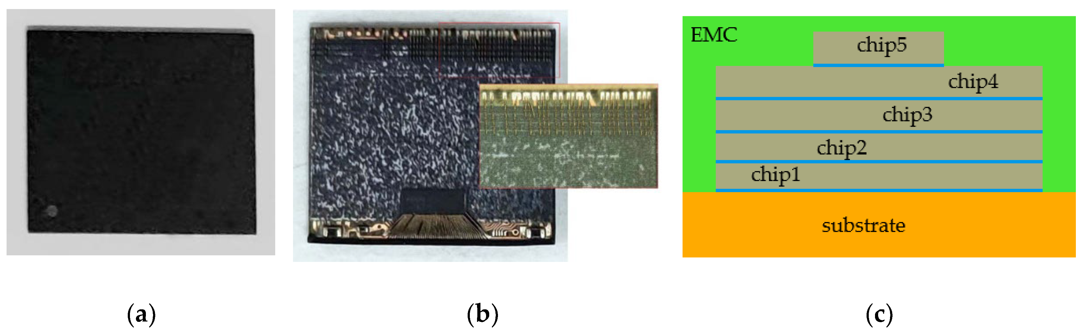
Figure 1.
Three-dimensional-stacked package memory chip structure. (a) Package outline; (b) laser decap package sample and its left-top corner detail picture; (c) package cross-section schematic (chips 1 to 4 are memory chips, and chip 5 is a main-control chip).
Figure 1.
Three-dimensional-stacked package memory chip structure. (a) Package outline; (b) laser decap package sample and its left-top corner detail picture; (c) package cross-section schematic (chips 1 to 4 are memory chips, and chip 5 is a main-control chip).

Figure 2.
EMC samples for DMA test.

Figure 3.
Single cantilever clamp in DMA.

Figure 4.
Storage modulus vs. temperature at different frequencies.

Figure 5.
Loss modulus vs. temperature at different frequencies.

Figure 6.
Storage modulus vs. frequency under different temperatures.

Figure 7.
The master curve of storage modulus for EMC sample.

Figure 8.
Shift factor scatter plot.

Figure 9.
Package material properties and FE grid.

Figure 10.
Temperature cyclic loading curve.

Figure 11.
Package deformation and stress cloud picture. (a) Package deformation cloud picture at high temperature; (b) package deformation cloud picture at low temperature; (c) package stress cloud picture at high temperature; (d) package stress cloud picture at low temperature.
Figure 11.
Package deformation and stress cloud picture. (a) Package deformation cloud picture at high temperature; (b) package deformation cloud picture at low temperature; (c) package stress cloud picture at high temperature; (d) package stress cloud picture at low temperature.

Figure 12.
Change in maximum stress in load cycle.

Figure 13.
Stress cloud picture of each layer of stacked chips. (a) Chip-1 stress cloud picture; (b) Chip-2 stress cloud picture; (c) Chip-3 stress cloud picture; (d) Chip-4 stress cloud picture; (e) Chip-5 stress cloud picture.
Figure 13.
Stress cloud picture of each layer of stacked chips. (a) Chip-1 stress cloud picture; (b) Chip-2 stress cloud picture; (c) Chip-3 stress cloud picture; (d) Chip-4 stress cloud picture; (e) Chip-5 stress cloud picture.

Figure 14.
Influence of EMC thickness on warpage.

Figure 15.
Influence of DAF on warpage. (a) Influence of DAF thickness on warpage; (b) influence of DAF CET on warpage.
Figure 15.
Influence of DAF on warpage. (a) Influence of DAF thickness on warpage; (b) influence of DAF CET on warpage.

Figure 16.
Influence of die thickness on warpage.


Table 1.
Packaging size and material parameters.
| Item | Material | Size (mm) | E (MPa) | v | A (ppm/°C) |
|---|---|---|---|---|---|
| EMC | EMC | 12 × 10 × 0.9 | Test | 0.3 | 9.38, T < Tg 38.68, T > Tg |
| Chip | Si | 10 × 8.0 × 0.1 | 131,000 | 0.3 | 2.8 |
| 10 × 7.8 × 0.1 | |||||
| 10 × 7.6 × 0.1 | |||||
| 10 × 7.4 × 0.1 | |||||
| 4 × 1.0 × 0.1 | |||||
| DA | DAF | 10 × 8.0 × 0.02 | 640@25 °C 140@150 °C | 0.4 | 48.00 |
| 10 × 7.8 × 0.02 | |||||
| 10 × 7.6 × 0.02 | |||||
| 10 × 7.4 × 0.02 | |||||
| 4 × 1.0 × 0.02 | |||||
| substrate | BT | 12 × 10 × 0.2 | X, Y: 26,000 Z: 11,000 | XZ, YZ: 0.39 XY: 0.11 | X, Y: 15 Z: 50 |
Note: X/Y/Z is material parameters in X/Y/Z direction.
Table 2.
Excitation frequency table for tensile mode DMA experiments.
| No. | 1 | 2 | 3 | 4 | 5 | 6 | 7 | 8 | 9 | 10 | 11 | 12 | 13 |
|---|---|---|---|---|---|---|---|---|---|---|---|---|---|
| Frequency (Hz) | 0.1 | 0.18 | 0.32 | 0.56 | 1 | 1.8 | 3.2 | 5.6 | 10 | 17.8 | 31.6 | 56 | 100 |
Table 3.
Viscoelastic material parameters of epoxy molding compound.
| No. | Relaxation Time τi (s) | Shear Relaxation Coefficient Gi | Volume Relaxation Coefficient Ki |
|---|---|---|---|
| τ1 | 1.00 × 10⁻⁸ | 239.32 | 518.54 |
| τ2 | 1.00 × 10⁻⁶ | 272.59 | 590.62 |
| τ3 | 1.00 × 10⁻⁴ | 354.33 | 767.71 |
| τ4 | 1.00 × 10⁻³ | 349.54 | 757.34 |
| τ5 | 1.00 × 10⁻² | 513.60 | 1112.8 |
| τ6 | 1.00 × 10⁻¹ | 966.29 | 2093.6 |
| τ7 | 1.00 × 100 | 853.56 | 1849.4 |
| τ8 | 1.00 × 101 | 1106.5 | 2397.4 |
| τ9 | 1.00 × 10² | 726.77 | 1574.6 |
| τ10 | 1.00 × 10³ | 560.19 | 1213.8 |
| τ11 | 1.00 × 10⁴ | 475.34 | 1029.7 |
| τ12 | 1.00 × 10⁶ | 305.22 | 662.19 |
| τ13 | 1.00 × 10⁸ | 87.513 | 183.44 |
| τ14 | 1.00 × 10⁹ | 150.87 | 342.30 |
Publisher’s Note: MDPI stays neutral with regard to jurisdictional claims in published maps and institutional affiliations. |
© 2022 by the authors. Licensee MDPI, Basel, Switzerland. This article is an open access article distributed under the terms and conditions of the Creative Commons Attribution (CC BY) license (https://creativecommons.org/licenses/by/4.0/).
Share and Cite
MDPI and ACS Style
Wang, X.; Cao, S.; Lu, G.; Yang, D. Viscoelastic Simulation of Stress and Warpage for Memory Chip 3D-Stacked Package. Coatings 2022, 12, 1976. https://doi.org/10.3390/coatings12121976
AMA Style
Wang X, Cao S, Lu G, Yang D. Viscoelastic Simulation of Stress and Warpage for Memory Chip 3D-Stacked Package. Coatings. 2022; 12(12):1976. https://doi.org/10.3390/coatings12121976
Chicago/Turabian StyleWang, Xiyou, Sicheng Cao, Guangsheng Lu, and Daoguo Yang. 2022. "Viscoelastic Simulation of Stress and Warpage for Memory Chip 3D-Stacked Package" Coatings 12, no. 12: 1976. https://doi.org/10.3390/coatings12121976
Note that from the first issue of 2016, this journal uses article numbers instead of page numbers. See further details here.