Article

Synthesis of ZnO/Bi2S3 Core/Shell Nanowire Array Photoanodes for Photocathodic Protection of Stainless Steel

School of Chemical Engineering and Technology, Sun Yat-sen University, Zhuhai 519082, China
*
Author to whom correspondence should be addressed.
Coatings 2022, 12(2), 244; https://doi.org/10.3390/coatings12020244
Submission received: 28 January 2022 / Revised: 9 February 2022 / Accepted: 11 February 2022 / Published: 13 February 2022
(This article belongs to the Special Issue Thin Films and Coatings for Energy Application)

Abstract

:
Nanocrystalline Bi2S3 shells were conformally deposited on ZnO nanowire arrays via a successive ionic layer adsorption and reaction approach. Microstructure, optical, and electric properties of the as-prepared ZnO/Bi2S3 core/shell nanowire heterostructures were thoroughly investigated using various characterization and electrochemical methods. Compared with the pristine ZnO photoanode (−734 mV and 0.57 mA·cm−2), the ZnO/Bi2S3 photoanode with a type-II heterojunction exhibited a more negative shift in the coupled open circuit potential (−862 mV) and a higher photocurrent density (2.92 mA·cm−2), achieving more effective photocathodic protections for the coupled 304 stainless steel under solar illumination.

1. Introduction

Protection of stainless steel against localized corrosion, such as pitting and crevice corrosion, is of great significance for its engineering applications [1,2,3]. Cathodic polarization is an effective strategy to suppress steel corrosion of marine and underground structures [1]. As a green alternative technique, photocathodic protection (PCP) is attracting tremendous scientific interests for steel anticorrosion by harnessing sustainable solar energy [2,4,5,6]. The present challenge of PCP is to exploit effective n-type semiconductor photoanodes to generate photoelectrons via photoelectric conversion effect and then transfer photoelectrons to the coupled steels [7,8,9,10]. Representatively, n-type TiO2 has been extensively investigated in the field of PCP, especially its composites with narrow-bandgap semiconductors [2,5,6,7,9,10,11,12,13,14,15,16,17,18]. Nevertheless, ZnO is significantly lagging behind TiO2 in PCP research though ZnO is one of the most promising candidates for PCP due to its conduction band negative enough, environmental benignity, and low cost [19,20,21]. To overcome the limitation of ZnO’s wide bandgap (~3.2 eV) and the corresponding UV-sensitive characteristic [22,23,24,25,26,27], nowadays, coupling ZnO with various narrow band gap semiconductors becomes indispensable for enhancing PEC properties in the visible light region [8,28,29,30,31,32,33,34,35,36].
Bi2S3 is a n-type semiconductor with a relatively narrow band gap (~1.3 eV) and is able to broaden the optical absorption range of ZnO to the visible part of solar light by hybridization [28,29,37]. More importantly, Bi2S3 possesses appropriate energy band alignments to form a type-II heterojunction with ZnO, which facilitates spatial charge separation via built-in electric field across the interface. Recently, ZnO/Bi2S3 heterostructures have been reported to reduce the recombination of charge carriers and enhance PEC properties [28,29,37,38,39,40,41,42,43], and moreover Bi2S3 has been also utilized to decorate TiO2 for improving PCP performances [11,18,44]. Therefore, it would be desirable to promote PCP performance of ZnO photoanodes for steels by rational introduction of Bi2S3. Just recently, Zhang et al. reported a Bi2S3/ZnO nanocomposite with a good PCP effect on 304 stainless steel (304 SS) [45]. However, the electrodeposited ZnO nanowires were poorly aligned, and their lengths were only ~300 nm, which dramatically restricted the photoinduced current density for PCP (0.094 mA·cm−2). To enhance the light absorption and increase the photoinduced current density, rational construction of Bi2S3/ZnO nanocomposites with the well-aligned ZnO nanowires of sufficient lengths will be promising for PCP.
In this study, ZnO/Bi2S3 core/shell heterostructured nanowire arrays were synthesized via a seed-assistant hydrothermal method followed by successive ionic layer adsorption and reaction (SILAR). Microstructure, optical, and electric properties of the as-prepared ZnO/Bi2S3 core/shell nanowire heterostructures were thoroughly investigated by X-ray diffraction (XRD), scanning electron microscopy (SEM), transmission electron microscope (TEM), energy dispersive X-ray spectroscopy (EDAX), X-ray photoelectron spectroscopy (XPS), ultraviolet–visible (UV–Vis), Electrochemical impedance spectroscopy (EIS), and Mott–Schottky plots. PCP performances of the ZnO/Bi2S3 photoanode for the coupled 304 SS were investigated in details.

2. Materials and Methods

2.1. Photoanode Synthesis

All chemicals were of analytical grade. ZnO nanowire arrays were synthesized by using a seed-assistant hydrothermal method [24]. Firstly, fluorine-doped tin oxide (FTO) conductive glasses were thoroughly cleaned by ultrasonic treatment in acetone, ethanol, and deionized water for 15 min, dried in an electrically heated convection oven at 90 °C, and treated before use with oxygen plasma for 3 min. Then, 100 μL of 25 mM zinc acetate aqueous solution was dropped on the cleaned FTO glasses and dried at 60 °C for 3 min. This drop-dry process was repeated 4 times. To form a thick ZnO seed layer, the pre-coated FTO glasses were calcined in a muffle furnace at 350 °C for 1 h with a heating rate of 5 °C·min−1. Lastly, ZnO-seeded FTO glasses were hydrothermally treated in a Teflon-lined stainless-steel autoclave filled with 50 mL of aqueous solution containing 2.5 mmol of ZnCl2 and 2.5 mmol of hexamethylenetetramine at 125 °C for 4 h. Deposition of particulate Bi2S3 on ZnO nanowire arrays was realized by a successive ionic layer adsorption and reaction (SILAR) method [11,18,44,46,47]. During each cycle, the substrates were immersed into separate Bi3+ and S2− precursor solutions for adsorption and reaction and subsequently rinsed with deionized water after each immersion to remove excess ions and hinder homogeneous precipitation. The absorption, reaction, and rinse times were 50, 60, and 30 s, respectively. The Bi3+ precursor solution contained 0.125 mmol of Bi(NO3)3 dissolved in 25 mL of ethylene glycol, and the S2− precursor solution contained 0.625 mmol of Na2S dissolved in 25 mL of deionized water. The substrates were dried at 85 °C for 5 min after each cycle, and optimal ten cycles of SILAR were implemented in total.

2.2. Characterization

Surface morphologies were observed by a field emission scanning electron microscope (FE-SEM, SU8020, Hitachi, Tokyo, Japan) operated at an accelerating voltage of 3 kV. Crystal phases were determined by a X-ray diffractometer (Ultima IV, Rigaku, Tokyo, Japan) with Cu Kα radiation (λ = 1.5418 Å). Surface chemical compositions and states were examined by a X-ray photoelectron spectrometer (ESCALAB 250Xi, Thermo, Waltham, MA, USA) with Al Kα radiation (hv = 1486.6 eV). Microstructures and elemental mappings were obtained by a high-resolution transmission electron microscope (HRTEM, Talos F200X, FEI, Lausanne, Switzerland) equipped with an energy dispersive X-ray spectroscopy (EDAX) detector. Optical absorption properties were investigated by an ultraviolet–visible (UV–Vis) spectrometer (UV-3600, Shimadzu, Tokyo, Japan).

2.3. Electrochemical Measurements

For photoelectrochemical measurements, a system comprised of an electrochemical workstation (CS350H, CorrTest, Wuhan, China) and a three-electrode cell was adopted (see the schematic diagram in our previous work [24]). The as-prepared photoanodes (1 cm × 1 cm) served as the work electrode, Pt foil as the counter electrode, and Ag/AgCl as the reference electrode. An aqueous solution of 0.2 M NaOH was used as the electrolyte, and 0.1 M Na2S was used as the hole scavenger. The simulated irradiation source was a 500 W xenon lamp (CHF-XM500, Perfectlight, Beijing, China) equipped with an AM 1.5 G filter, and the light intensity was fixed at 100 mW·cm−2 using an optical power meter (PL-MW2000, Perfectlight, Beijing, China). The open circuit potential (OCP) measurements were conducted in a H-type electrochemical cell separated with a Nafion membrane between two chambers [24]. The as-prepared photoanodes were electrically connected with 304 SS placed in another chamber containing 3.5 wt. % NaCl aqueous solution. Electrochemical impedance spectroscopy (EIS, 10−2~105 Hz) and Mott–Schottky measurements (100 Hz) were performed on a Gamry Interface 1010E electrochemical workstation with 10 mV alternating current amplitude under dark.

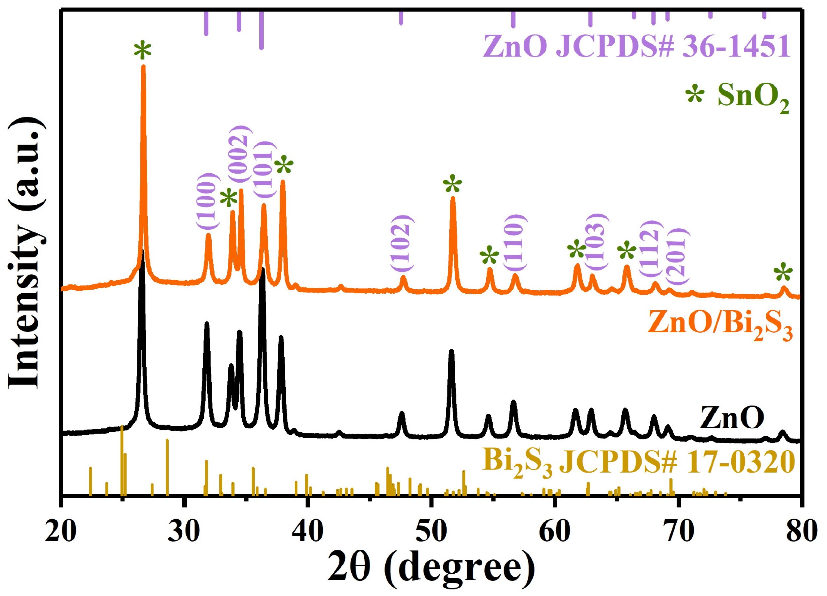
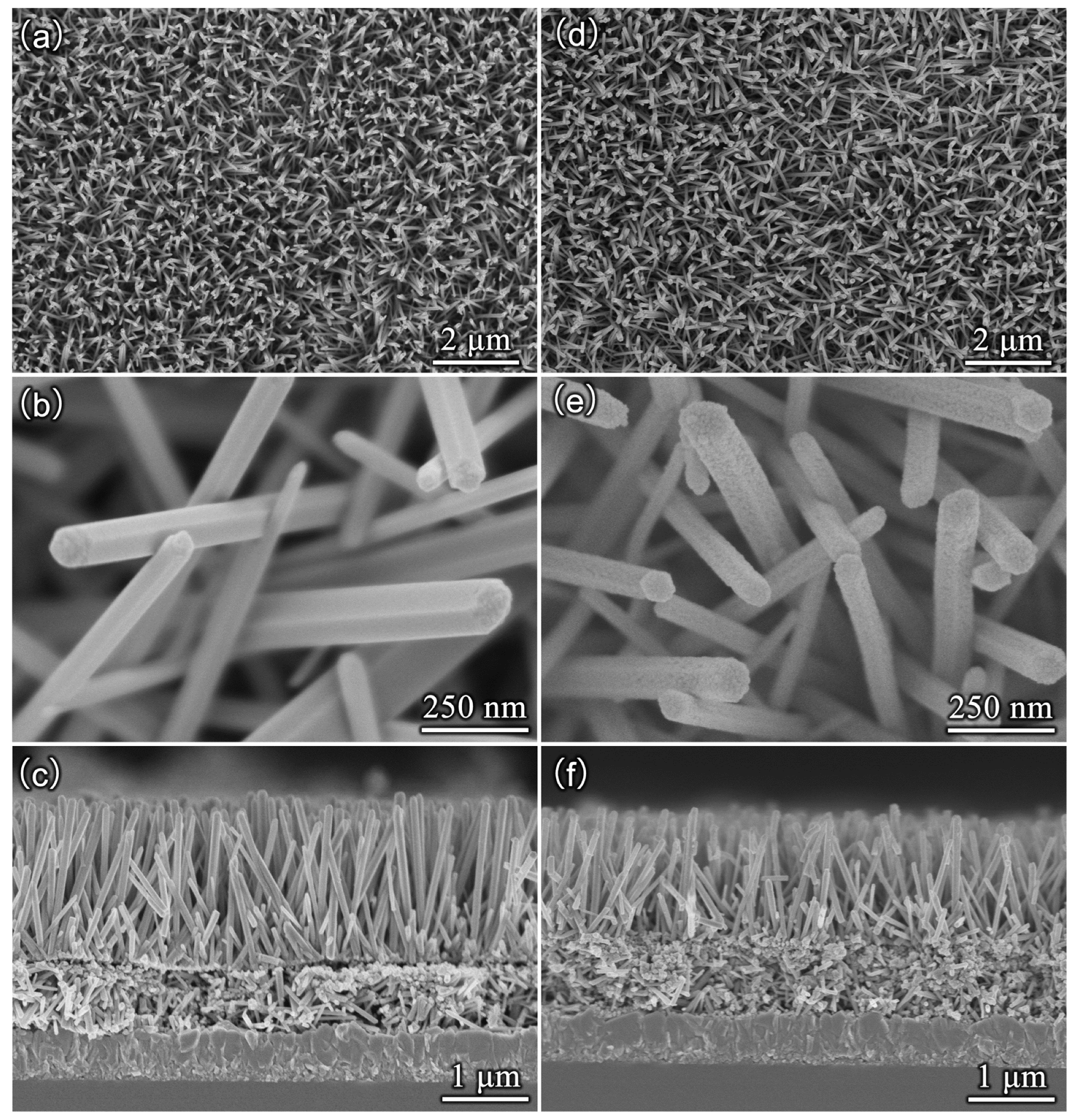
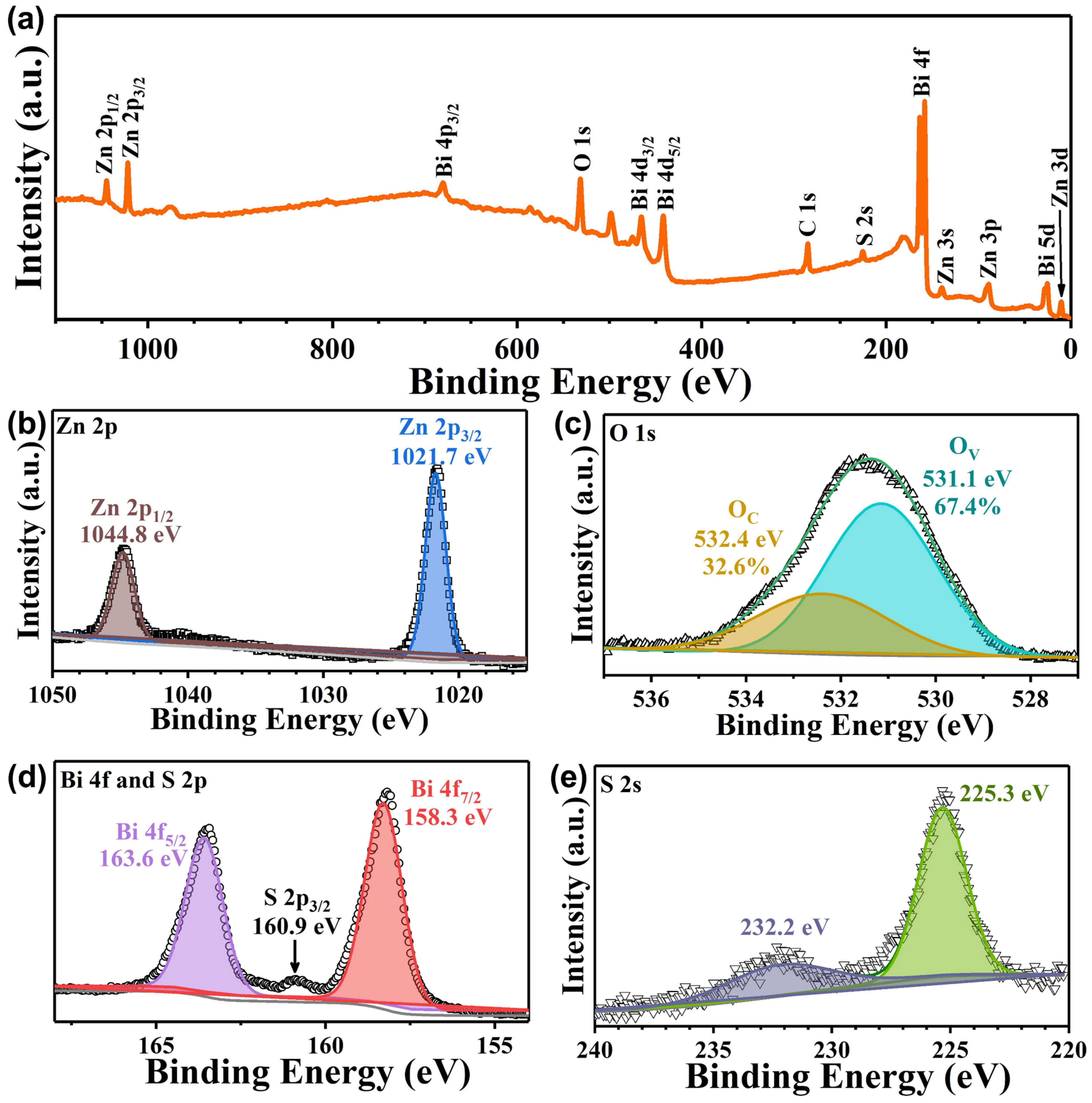
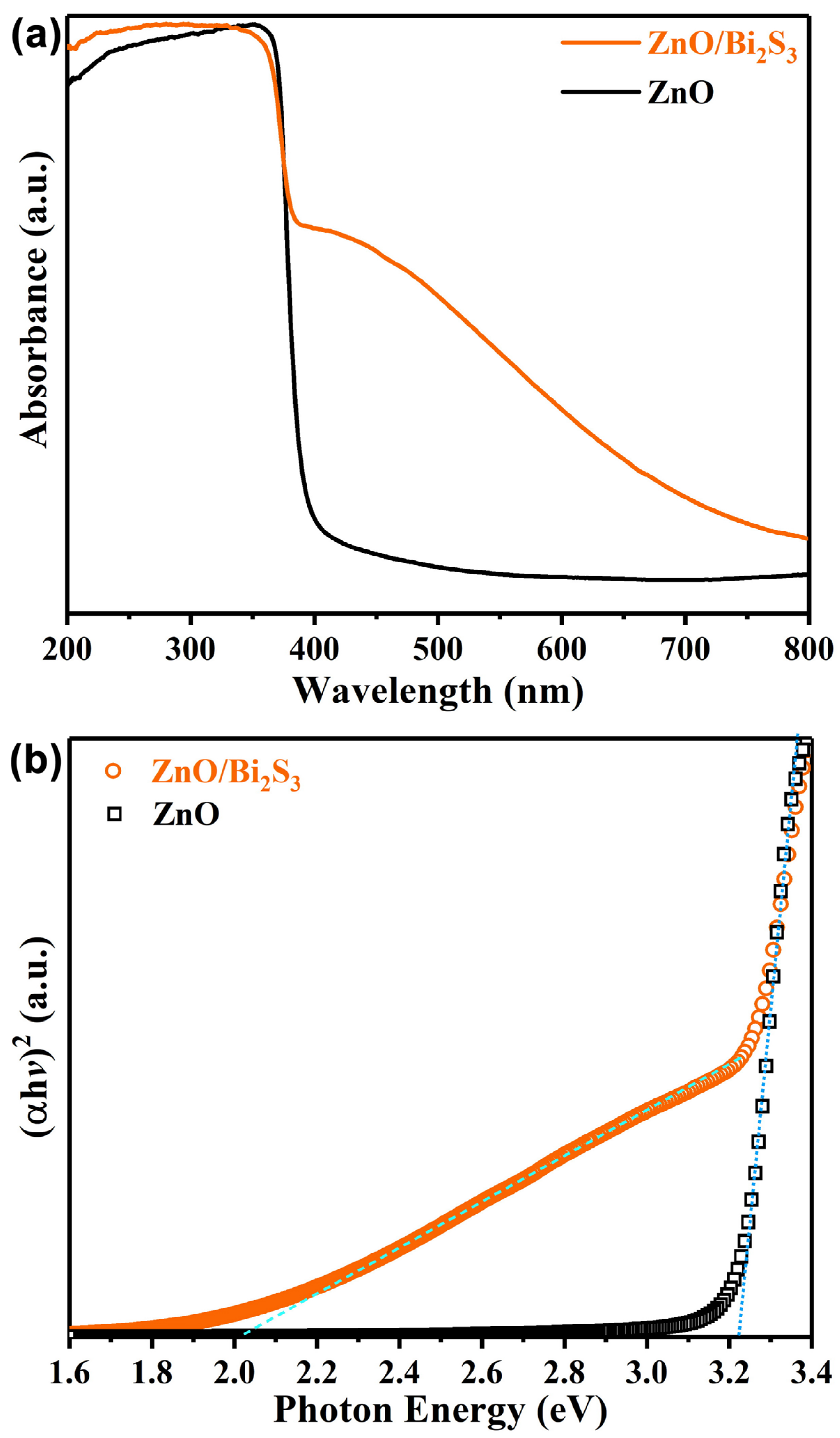
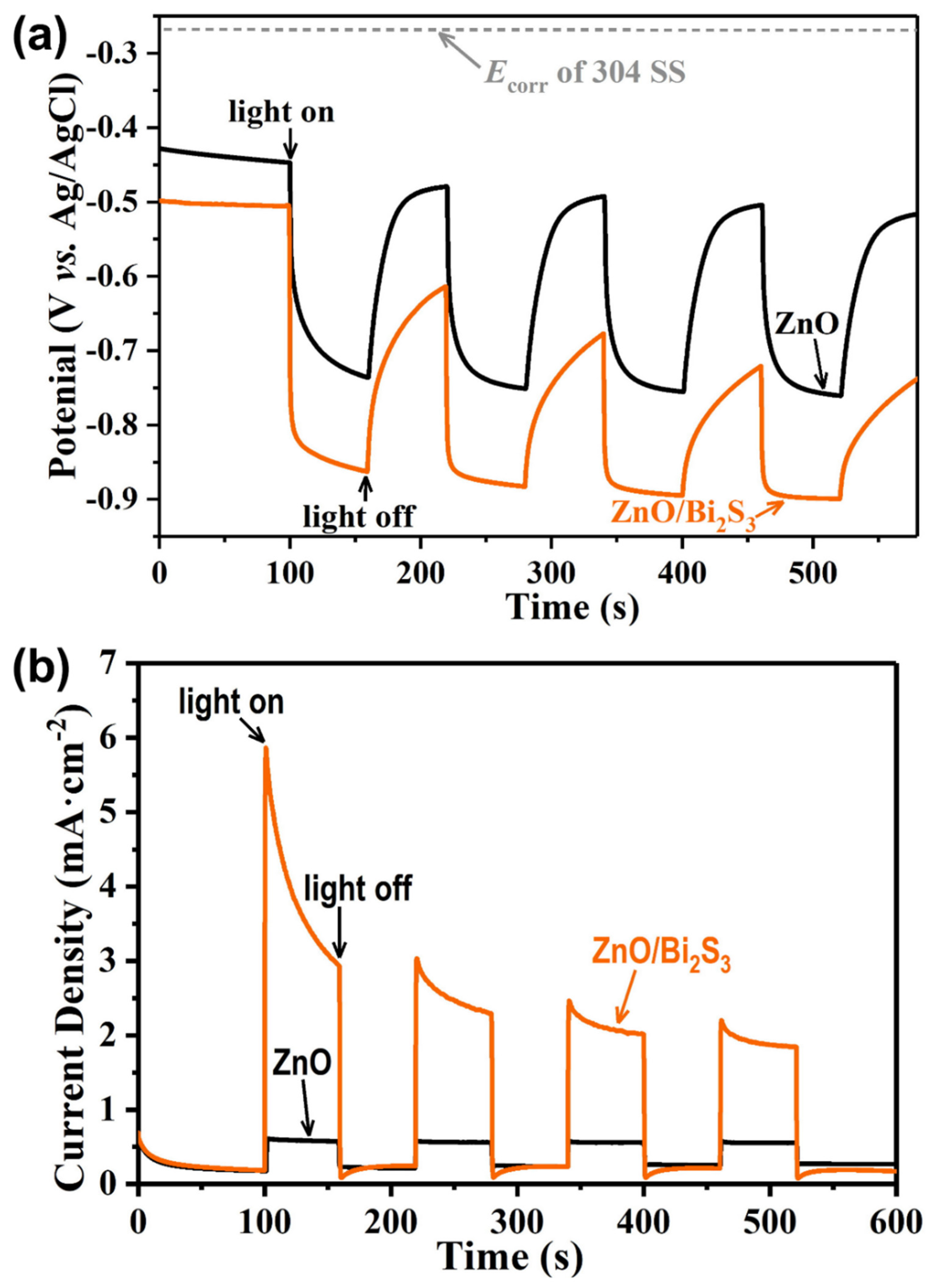
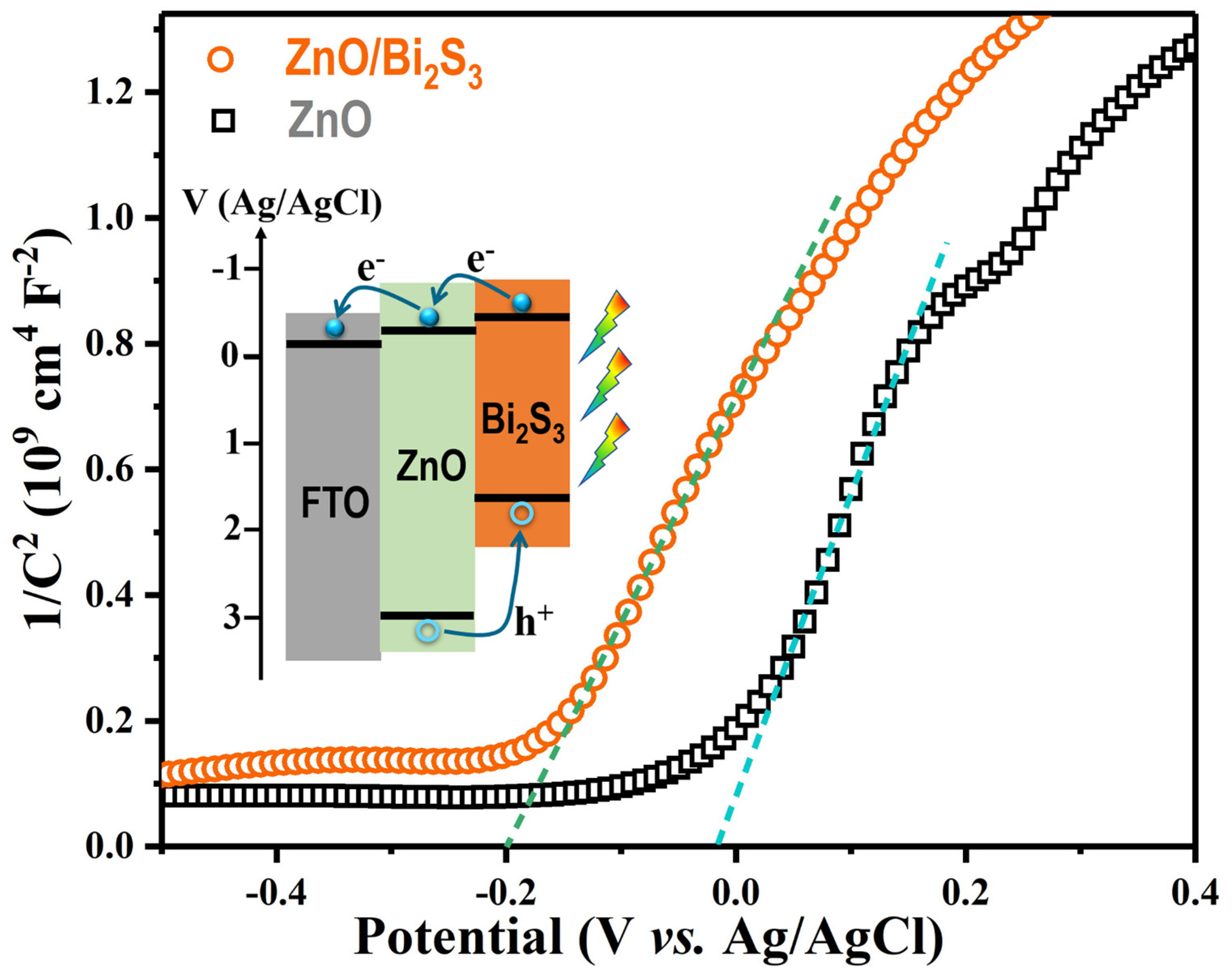
3. Results and Discussion

Crystal phases of the as-prepared ZnO/Bi2S3 core/shell nanowire arrays were analyzed by powder XRD patterns in Figure 1. For the ZnO photoanode, the collected diffraction peaks can be divided into two groups. One group of diffraction peak located at 31.8°, 34.4°, 36.3°, 47.5°, 56.6°, 62.9°, 68.0°, and 69.1° matched well with (100), (002), (101), (102), (110), (103), (112), and (201) reflections of hexagonal ZnO (JCPDS# 36-1451) [22,24]. Another group of diffraction peak centered at 26.6°, 33.9°, 37.9°, 51.8°, 54.8°, 61.9°, 65.9°, and 78.7° was indexed to (110), (101), (200), (211), (220), (310), (301), and (321) reflections of tetragonal SnO2 (JCPDS# 41-1445) from FTO conductive glasses. After coating with Bi2S3 on ZnO via the SILAR method, no additional diffraction peak was detected in the ZnO/Bi2S3 photoanode. For instance, there was no peak for orthorhombic Bi2S3 (JCPDS# 17-0320) in Figure 1. The absence of Bi2S3 reflection may be caused by the poor crystallinity and low content of Bi2S3.
Figure 2 shows the representative SEM images of ZnO and ZnO/Bi2S3 photoanodes. The ZnO/Bi2S3 photoanode exhibited similar surface morphologies with the ZnO photoanode. Dense nanowires with the lengths between 1.5 and 2.1 μm and the diameters between 35 and 150 nm were vertically aligned and uniformly distributed on the entire FTO substrate. It was noted that the surface of nanowires changes from smooth for the pristine ZnO (Figure 2b) to rough for the Bi2S3 overcoated ZnO (Figure 2e). Obviously, a great number of Bi2S3 nanoparticles [48] are tightly deposited on the outer wall of ZnO nanowires so that ZnO nanowire cores are successfully covered by conformal Bi2S3 shells.
The information of microstructures and composition distributions was obtained by HRTEM and EDAX elemental mappings. Figure 3a shows a typical core/shell structured nanowire with a diameter of ~100 nm and a highly porous shell composed of nanoparticles. In the lattice-resolved TEM image (Figure 3b), the lattice fringe with an interplane spacing of 0.261 nm is ascribed to the (002) plane of ZnO from the nanowire core. Importantly, a distinct interplane spacing of 0.33 nm was clearly observed, which can be attributed to the (021) crystal plane of orthorhombic Bi2S3 (JCPDS# 17-0320) [11,18,44,47]. Near the outermost wall of the nanowire, lattice fringes show short-range order and long-range disorder, which is the characteristic of nanocrystalline or amorphous Bi2S3. These analyses support the absence of Bi2S3 diffraction peaks in the XRD pattern. The core/shell nanostructure was further unveiled by STEM and the corresponding elemental mapping images in Figure 3c–g. The Zn and O elements were mostly constrained in the nanowire core, while the Bi and S elements were mostly distributed in the shell region. The merged image of Zn, O, Bi, and S elements in Figure 3h displays that the core/shell nanowire has a shell thickness of ~15 nm. In brief, both HRTEM and EDAX analyses demonstrate the successful coating of the nanocrystalline Bi2S3 shell on the ZnO nanowire core.
Chemical compositions and states of the ZnO/Bi2S3 photoanode were studied by X-ray photoelectron spectroscopy (XPS). The survey spectrum in Figure 4a reveals the existence of various bind energies from Zn, O, Bi, and S elements. The high-resolution Zn 2p spectrum in Figure 4b displays two peaks centered at 1021.7 and 1044.8 eV, ascribing to Zn 2p3/2 and Zn 2p1/2 of Zn2+, respectively. In Figure 4c, the predominant O 1s spectrum can be deconvoluted into two peaks located at 531.1 and 532.4 eV, corresponding to oxygen vacancies and chemisorbed oxygen, respectively [24,49]. In the Bi 4f spectrum (Figure 4d), two main peaks at 158.3 and 163.6 eV are attributed to Bi 4f5/2 and Bi 4f7/2 of Bi3+, respectively. The remained peak at 160.9 eV in Figure 4d is related to S 2p3/2. The S 2s peak at 225.3 eV (Figure 4e) further proves the presence of S2− [50,51]. The appearance of S 2s peak at 232.2 eV is indicative of the formation of sulfates (SO42−), arising from the hydrolysis of sulfides [50]. Therefore, XPS analyses prove the presence of Bi3+ and S2−, suggesting the formation of Bi2S3 on the surface of nanowires.
Figure 5a shows the optical absorption properties of ZnO and ZnO/Bi2S3 photoanodes measured via UV–Vis spectroscopy. It was seen that the ZnO photoanode can only absorb UV light with an absorption edge at 385 nm. Obtained from the slope in Tauc plots of (αhv)2 to photo energy (Figure 5b), the band gap value of the ZnO photoanode was 3.22 eV. By contrast, the absorption edge of the ZnO/Bi2S3 photoanode was extended to 614 nm, indicating an optical band gap of 2.02 eV. Obviously, the ZnO/Bi2S3 photoanode exhibits a significantly enhanced absorption capability in the visible part of solar spectrum when Bi2S3 is composited with ZnO.
To understand the PCP performance of the ZnO/Bi2S3 photoanode, the photoinduced open circuit potential (OCP) variation of coupled 304 SS and transient photocurrent responses were measured under intermittent illumination of simulated solar light (AM 1.5 G). As shown in Figure 6a, OCP of 304 SS moderately shifts to the negative direction in the dark while coupled with the ZnO and ZnO/Bi2S3 photoanodes. Once exposed to white light, the ZnO/Bi2S3 photoanode shows a dramatical shift to −862 mV in the couped OCP, suggesting a better PCP performance than the ZnO photoanode (−734 mV). According to the large photoinduced potential drop, it is speculated that the photoelectrons of ZnO/Bi2S3 photoanode excited from its valence band maximum (VBM) to conduction band minimum (CBM) by white light can be transferred to the connected 304 SS for efficient cathodic polarization and protection. Figure 6b exhibits positive photocurrent responses for the ZnO and ZnO/Bi2S3 photoanodes, characteristic of PCP for 304 SS. Importantly, the ZnO/Bi2S3 photoanode (2.92 mA·cm−2) presents five times higher photocurrent than the ZnO photoanode (0.57 mA·cm−2) in the final of first cycle, demonstrating a better PCP performance than the just-reported ZnO/Bi2S3 nanocomposites (0.094 mA·cm−2) [45].
Figure 7 displays a long-term photoinduced OCP variation of 304 SS coupled with the ZnO/Bi2S3 photoanode. Under continuous illumination of simulated solar light, OCP of the ZnO/Bi2S3 photoanodes coupled with 304 SS was stabilized at −0.9 V for 6 h, validating a superior PCP durability for 304 SS.
To obtain the flat-band potentials of ZnO and ZnO/Bi2S3 photoanodes, Mott–Schottky plots were recorded at an applied frequency of 100 Hz in the dark. The linear fitting of Mott–Schottky plots in Figure 8 shows positive slopes, typical of n-type semiconductors [52,53]. Based on the x-axis intercepts of the fitted tangent lines, the flat-band potentials of ZnO and ZnO/Bi2S3 photoanodes were estimated to be approximately −0.01 and −0.20 V vs. Ag/AgCl, respectively. Thus, the CBM values of n-type ZnO and Bi2S3 can be considered as −0.21 and −0.40 V, respectively [52,53]. In terms of the optical band gaps, VBM of n-type ZnO and Bi2S3 can be speculated at 3.01 and 1.62 V, respectively. As shown in the inset, a type-II semiconductor heterojunction was constructed between ZnO and Bi2S3, which is beneficial for the spatial charge separation in the ZnO/Bi2S3 photoanode. Clearly, hybridization of Bi2S3 with ZnO not only broadens the absorption spectrum but also increases the charge separation efficiency, which is of great importance to boost PCP performances of the ZnO/Bi2S3 photoanode.
To investigate the charge transfer properties, EIS was used to record Nyquist plots of the ZnO and ZnO/Bi2S3 photoanodes under the dark. Generally, the charge transfer resistance (Rct) can be estimated from the diameter of the semicircle in the high-frequency region, and a smaller radius of impedance arc indicates a more decreased Rct [22,23]. As fitted by EClab software using the proposed equivalent circuit model (see the inset in Figure 9), the Rct value of ZnO/Bi2S3 photoanode was 12.7 kΩ, which was much smaller than that of the ZnO photoanode (50.8 kΩ). Therefore, the ZnO/Bi2S3 photoanode exhibits the significantly improved charge transfer kinetics, resulting in the enhanced PCP performance.

4. Conclusions

In summary, Bi2S3 was successfully deposited on ZnO nanowire arrays via a SILAR approach. The as-prepared ZnO/Bi2S3 core/shell nanowire heterostructures were thoroughly investigated by XRD, SEM, TEM, EDAX, XPS, UV–Vis, EIS, and Mott–Schottky plots. Compared with the ZnO photoanode (385 nm, −734 mV, and 0.57 mA·cm−2), the ZnO/Bi2S3 photoanode with a type-II heterojunction exhibited an optical absorption red-shift (614 nm), a more negative shift in the coupled OCP (−862 mV), and a higher photocurrent density (2.92 mA·cm−2), achieving more effective photocathodic protections for the coupled 304 SS under solar illumination.

Author Contributions

Methodology, formal analysis, investigation, and data curation, Y.L.; conceptualization, writing, visualization, supervision, project administration, and funding acquisition, S.L. All authors have read and agreed to the published version of the manuscript.

Funding

This research was funded by the “Hundred Talent Program” from Sun Yat-sen University.

Institutional Review Board Statement

Not applicable.

Informed Consent Statement

Not applicable.

Data Availability Statement

The authors confirm that the data supporting the findings of this study are available within the article.

Conflicts of Interest

The authors declare no conflict of interest.

References

  1. Lo, K.H.; Shek, C.H.; Lai, J.K.L. Recent developments in stainless steels. Mat. Sci. Eng. R 2009, 65, 39–104. [Google Scholar] [CrossRef]
  2. Ma, X.; Ma, Z.; Lu, D.; Jiang, Q.; Li, L.; Liao, T.; Hou, B. Enhanced photoelectrochemical cathodic protection performance of MoS2/TiO2 nanocomposites for 304 stainless steel under visible light. J. Mater. Sci. Technol. 2021, 64, 21–28. [Google Scholar] [CrossRef]
  3. Zhang, J.; Yang, H.; Wang, Y.; Cui, X.; Wen, Z.; Liu, Y.; Fan, L.; Feng, J. Facile fabrication of SnO2 modified TiO2 nanorods film for efficient photocathodic protection of 304 stainless steel under simulated solar light. Corros. Sci. 2020, 176, 108927. [Google Scholar] [CrossRef]
  4. Bu, Y.; Ao, J.-P. A review on photoelectrochemical cathodic protection semiconductor thin films for metals. Green Energy Environ. 2017, 2, 331–362. [Google Scholar] [CrossRef]
  5. Wang, N.; Wang, J.; Liu, M.; Ge, C.; Hou, B.; Liu, N.; Ning, Y.; Hu, Y. Preparation of FeS2/TiO2 nanocomposite films and study on the performance of photoelectrochemistry cathodic protection. Sci. Rep. 2021, 11, 7509. [Google Scholar] [CrossRef] [PubMed]
  6. Wang, C.; Gao, W.; Liu, N.; Xin, Y.; Liu, X.; Wang, X.; Tian, Y.; Chen, X.; Hou, B. Covalent organic framework decorated TiO2 nanotube arrays for photoelectrochemical cathodic protection of steel. Corros. Sci. 2020, 176, 108920. [Google Scholar] [CrossRef]
  7. Yang, Y.; Cheng, Y.F. Visible light illuminated high-performance WO3-TiO2-BiVO4 nanocomposite photoanodes capable of energy self-storage for photo-induced cathodic protection. Corros. Sci. 2020, 164, 108333. [Google Scholar] [CrossRef]
  8. Wei, N.; Lin, Y.; Li, Z.; Sun, W.; Zhang, G.; Wang, M.; Cui, H. One-dimensional Ag2S/ZnS/ZnO nanorod array films for photocathodic protection for 304 stainless steel. J. Mater. Sci. Technol. 2020, 42, 156–162. [Google Scholar] [CrossRef]
  9. Jiang, X.; Sun, M.; Chen, Z.; Jing, J.; Feng, C. High-efficiency photoelectrochemical cathodic protection performance of the TiO2/AgInSe2/In2Se3 multijunction nanosheet array. Corros. Sci. 2020, 176, 108901. [Google Scholar] [CrossRef]
  10. Sun, W.; Wei, N.; Cui, H.; Lin, Y.; Wang, X.; Tian, J.; Li, J.; Wen, J. 3D ZnIn2S4 nanosheet/TiO2 nanowire arrays and their efficient photocathodic protection for 304 stainless steel. Appl. Surf. Sci. 2018, 434, 1030–1039. [Google Scholar] [CrossRef]
  11. Jin, P.; Guan, Z.-C.; Wang, H.-P.; Wang, X.; Liu, G.-K.; Du, R.-G. Bi2S3/rGO co-modified TiO2 nanotube photoanode for enhanced photoelectrochemical cathodic protection of stainless steel. J. Photochem. Photobiol. A 2021, 407, 113060. [Google Scholar] [CrossRef]
  12. Jiang, X.; Sun, M.; Chen, Z.; Jing, J.; Lu, G.; Feng, C. Boosted photoinduced cathodic protection performance of ZnIn2S4/TiO2 nanoflowerbush with efficient photoelectric conversion in NaCl solution. J. Alloys Compd. 2021, 876, 160144. [Google Scholar] [CrossRef]
  13. Xu, D.; Yang, M.; Liu, Y.; Zhu, R.; Lv, X.; Zhang, C.; Liu, B. Fabrication of an innovative designed TiO2 nanosheets/CdSe/polyaniline/graphene quaternary composite and its application as in-situ photocathodic protection coatings on 304SS. J. Alloys Compd. 2020, 822, 153685. [Google Scholar] [CrossRef]
  14. Ma, Z.; Ma, X.; Liu, N.; Wang, X.; Wang, L.; Hou, B. Study on the photocathodic protection of 304 stainless steel by Ag and In2S3 co-sensitized TiO2 composite. Appl. Surf. Sci. 2020, 507, 145088. [Google Scholar] [CrossRef]
  15. Jiang, X.; Sun, M.; Chen, Z.; Jing, J.; Feng, C. An ultrafine hyperbranched CdS/TiO2 nanolawn photoanode with highly efficient photoelectrochemical performance. J. Alloys Compd. 2020, 816, 152533. [Google Scholar] [CrossRef]
  16. Li, H.; Li, Y.; Wang, X.; Hou, B. 3D ZnIn2S4 nanosheets/TiO2 nanotubes as photoanodes for photocathodic protection of Q235 CS with high efficiency under visible light. J. Alloys Compd. 2019, 771, 892–899. [Google Scholar] [CrossRef]
  17. Li, X.; Wang, X.; Ning, X.; Lei, J.; Shao, J.; Wang, W.; Huang, Y.; Hou, B. Sb2S3/Sb2O3 modified TiO2 photoanode for photocathodic protection of 304 stainless steel under visible light. Appl. Surf. Sci. 2018, 462, 155–163. [Google Scholar] [CrossRef]
  18. Hu, J.; Guan, Z.-C.; Liang, Y.; Zhou, J.-Z.; Liu, Q.; Wang, H.-P.; Zhang, H.; Du, R.-G. Bi2S3 modified single crystalline rutile TiO2 nanorod array films for photoelectrochemical cathodic protection. Corros. Sci. 2017, 125, 59–67. [Google Scholar] [CrossRef]
  19. Kale, V.; Hunge, Y.M.; Kamble, S.A.; Deshmukh, M.; Bhoraskar, S.V.; Mathe, V.L. Modification of energy level diagram of nano-crystalline ZnO by its composites with ZnWO4 suitable for sunlight assisted photo catalytic activity. Mater. Today Commun. 2021, 26, 102101. [Google Scholar] [CrossRef]
  20. Hunge, Y.M.; Yadav, A.A.; Mathe, V.L. Ultrasound assisted synthesis of WO3-ZnO nanocomposites for brilliant blue dye degradation. Ultrason. Sonochem. 2018, 45, 116–122. [Google Scholar] [CrossRef]
  21. Hunge, Y.M.; Yadav, A.A.; Kulkarni, S.B.; Mathe, V.L. A multifunctional ZnO thin film based devices for photoelectrocatalytic degradation of terephthalic acid and CO2 gas sensing applications. Sensors Actuat. B Chem. 2018, 274, 1–9. [Google Scholar] [CrossRef]
  22. Yang, Y.; Cheng, Y.F. One-step facile preparation of ZnO nanorods as high-performance photoanodes for photoelectrochemical cathodic protection. Electrochim. Acta 2018, 276, 311–318. [Google Scholar] [CrossRef]
  23. Liu, Y.; Zhu, Z.; Cheng, Y. An in-depth study of photocathodic protection of SS304 steel by electrodeposited layers of ZnO nanoparticles. Surf. Coat. Technol. 2020, 399, 126158. [Google Scholar] [CrossRef]
  24. Lin, Y.; Liu, S. Robust ZnO nanowire photoanodes with oxygen vacancies for efficient photoelectrochemical cathodic protection. Appl. Surf. Sci. 2021, 566, 150694. [Google Scholar] [CrossRef]
  25. Sun, M.; Chen, Z.; Bu, Y.; Yu, J.; Hou, B. Effect of ZnO on the corrosion of zinc, Q235 carbon steel and 304 stainless steel under white light illumination. Corros. Sci. 2014, 82, 77–84. [Google Scholar] [CrossRef]
  26. Techapiesancharoenkij, R.; Sripianem, W.; Tongpul, K.; Peamjharean, C.; Wichean, T.N.; Meesak, T.; Eiamchai, P. Investigation of the photocathodic protection of a transparent ZnO coating on an AISI type 304 stainless steel in a 3% NaCl solution. Surf. Coat. Technol. 2017, 320, 97–102. [Google Scholar] [CrossRef]
  27. Wang, H.; Xie, J.; Jiang, X.; Zhu, Z.; Wang, Y.; Chamas, M.; Duan, M.; Tang, J. Photoelectrochemical Behavior of Microrod ZnO Coated 316L Stainless Steel Prepared by Hydrothermal Method. Int. J. Electrochem. Sc. 2016, 11, 10278–10286. [Google Scholar] [CrossRef]
  28. Das Mahapatra, A.; Basak, D. Enhanced ultraviolet photosensing properties in Bi2S3 nanoparticles decorated ZnO nanorods’ heterostructure. J. Alloys Compd. 2019, 797, 766–774. [Google Scholar] [CrossRef]
  29. Xitao, W.; Rong, L.; Kang, W. Synthesis of ZnO@ZnS-Bi2S3 core-shell nanorod grown on reduced graphene oxide sheets and its enhanced photocatalytic performance. J. Mater. Chem. A 2014, 2, 8304–8313. [Google Scholar] [CrossRef]
  30. Zhang, G.; Chen, D.; Li, N.; Xu, Q.; Li, H.; He, J.; Lu, J. Fabrication of Bi2MoO6/ZnO hierarchical heterostructures with enhanced visible-light photocatalytic activity. Appl. Catal. B-Environ. 2019, 250, 313–324. [Google Scholar] [CrossRef]
  31. Wang, S.; Zhu, B.; Liu, M.; Zhang, L.; Yu, J.; Zhou, M. Direct Z-scheme ZnO/CdS hierarchical photocatalyst for enhanced photocatalytic H2-production activity. Appl. Catal. B-Environ. 2019, 243, 19–26. [Google Scholar] [CrossRef]
  32. Nie, N.; Zhang, L.; Fu, J.; Cheng, B.; Yu, J. Self-assembled hierarchical direct Z-scheme g-C3N4/ZnO microspheres with enhanced photocatalytic CO2 reduction performance. Appl. Surf. Sci. 2018, 441, 12–22. [Google Scholar] [CrossRef]
  33. Li, N.; Tian, Y.; Zhao, J.; Zhang, J.; Zuo, W.; Kong, L.; Cui, H. Z-scheme 2D/3D g-C3N4@ZnO with enhanced photocatalytic activity for cephalexin oxidation under solar light. Chem. Eng. J. 2018, 352, 412–422. [Google Scholar] [CrossRef]
  34. Wang, D.; Han, D.; Shi, Z.; Wang, J.; Yang, J.; Li, X.; Song, H. Optimized design of three-dimensional multi-shell Fe3O4/SiO2/ZnO/ZnSe microspheres with type II heterostructure for photocatalytic applications. Appl. Catal. B Environ. 2018, 227, 61–69. [Google Scholar] [CrossRef]
  35. Jiang, Y.; Liao, J.-F.; Xu, Y.-F.; Chen, H.-Y.; Wang, X.-D.; Kuang, D.-B. Hierarchical CsPbBr3 nanocrystal-decorated ZnO nanowire/macroporous graphene hybrids for enhancing charge separation and photocatalytic CO2 reduction. J. Mater. Chem. A 2019, 7, 13762–13769. [Google Scholar] [CrossRef]
  36. Li, M.; Tu, X.; Wang, Y.; Su, Y.; Hu, J.; Cai, B.; Lu, J.; Yang, Z.; Zhang, Y. Highly Enhanced Visible-Light-Driven Photoelectrochemical Performance of ZnO-Modified In2S3 Nanosheet Arrays by Atomic Layer Deposition. Nano-Micro Lett. 2018, 10, 45. [Google Scholar] [CrossRef] [Green Version]
  37. Sadhasivam, S.; Anbarasan, N.; Mukilan, M.; Manivel, P.; Jeganathan, K. Bi2S3 anchored ZnS/ZnO nanorod arrays photoanode for enhanced visible light driven photo electrochemical properties. Int. J. Hydrogen Energy 2020, 45, 30080–30090. [Google Scholar] [CrossRef]
  38. Sun, X.; Wu, H.; Tang, Y.; Zheng, Z.; Li, Y.; Li, L.; Zhang, Q. Enhanced photoelectrocatalytic degradation of tetrabromobisphenol a from tip-decorated ZnO nanorod electrode with Bi2S3 nanoparticles. Mater. Sci. Semicond. Process. 2021, 128, 105724. [Google Scholar] [CrossRef]
  39. Chen, P.; Gu, L.; Cao, X. From single ZnO multipods to heterostructured ZnO/ZnS, ZnO/ZnSe, ZnO/Bi2S3 and ZnO/Cu2S multipods: Controlled synthesis and tunable optical and photoelectrochemical properties. CrystEngComm 2010, 12, 3950–3958. [Google Scholar] [CrossRef]
  40. Balachandran, S.; Swaminathan, M. The simple, template free synthesis of a Bi2S3-ZnO heterostructure and its superior photocatalytic activity under UV-A light. Dalton T 2013, 42, 5338–5347. [Google Scholar] [CrossRef] [PubMed]
  41. Du, X.; Shi, R.; Ma, Y.; Cai, F.; Wang, X.; Yuan, Z. Enhanced thermoelectric performance of n-type Bi2S3 with added ZnO for power generation. RSC Adv. 2015, 5, 31004–31009. [Google Scholar] [CrossRef]
  42. Bera, S.; Ghosh, S.; Basu, R.N. Fabrication of Bi2S3/ZnO heterostructures: An excellent photocatalyst for visible-light-driven hydrogen generation and photoelectrochemical properties. New J. Chem. 2018, 42, 541–554. [Google Scholar] [CrossRef]
  43. Velanganni, S.; Manikandan, A.; Prince, J.J.; Mohan, C.N.; Thiruneelakandan, R. Nanostructured ZnO coated Bi2S3 thin films: Enhanced photocatalytic degradation of methylene blue dye. Phys. B 2018, 545, 383–389. [Google Scholar] [CrossRef]
  44. Li, H.; Wang, X.; Wei, Q.; Hou, B. Photocathodic protection of 304 stainless steel by Bi2S3/TiO2 nanotube films under visible light. Nanoscale Res. Lett. 2017, 12, 80. [Google Scholar] [CrossRef] [PubMed] [Green Version]
  45. Zhang, Y.; Bao, H.; Liu, X.; Zhang, X.; He, H.; Li, T.; Yang, H.; Shah, S.P.; Li, W. Bi2S3 nanoparticles/ZnO nanowire heterojunction films for improved photoelectrochemical cathodic protection for 304 SS under visible light. J. Appl. Electrochem. 2022, 52, 559–571. [Google Scholar] [CrossRef]
  46. Majumder, S.; Quang, N.D.; Kim, C.; Kim, D. Anion exchange and successive ionic layer adsorption and reaction-assisted coating of BiVO4 with Bi2S3 to produce nanostructured photoanode for enhanced photoelectrochemical water splitting. J. Colloid Interface Sci. 2021, 585, 72–84. [Google Scholar] [CrossRef] [PubMed]
  47. Wang, Q.; Liu, Z.; Jin, R.; Wang, Y.; Gao, S. SILAR preparation of Bi2S3 nanoparticles sensitized TiO2 nanotube arrays for efficient solar cells and photocatalysts. Sep. Purif. Technol. 2019, 210, 798–803. [Google Scholar] [CrossRef]
  48. Kang, L.; Shi, L.; Zeng, Q.; Liao, B.; Wang, B.; Guo, X. Melamine resin-coated lignocellulose fibers with robust superhydrophobicity for highly effective oil/water separation. Sep. Purif. Technol. 2021, 279, 119737. [Google Scholar] [CrossRef]
  49. Xu, D.; Liu, Y.; Zhang, Y.; Shi, Z.; Yang, M.; Zhang, C.; Liu, B. Fabrication of pyramid-BiVO4/CdSe composite with controlled surface oxygen vacancies boosting efficient carriers’ separation for photocathodic protection. Chem. Eng. J. 2020, 393, 124693. [Google Scholar] [CrossRef]
  50. Zingg, D.S.; Hercules, D.M. Electron spectroscopy for chemical analysis studies of lead sulfide oxidation. J. Phys. Chem. 1978, 82, 1992–1995. [Google Scholar] [CrossRef]
  51. Malakooti, R.; Cademartiri, L.; Akçakir, Y.; Petrov, S.; Migliori, A.; Ozin, G.A. Shape-controlled Bi2S3 nanocrystals and their plasma polymerization into flexible films. Adv. Mater. 2006, 18, 2189–2194. [Google Scholar] [CrossRef]
  52. Jing, J.; Chen, Z.; Bu, Y.; Sun, M.; Zheng, W.; Li, W. Significantly enhanced photoelectrochemical cathodic protection performance of hydrogen treated Cr-doped SrTiO3 by Cr6+ reduction and oxygen vacancy modification. Electrochim. Acta 2019, 304, 386–395. [Google Scholar] [CrossRef]
  53. Kuang, S.; Zheng, W.; Gu, Y.; Sun, Z.; Yang, Z.; Li, W.; Feng, C. Dual-functional ZnxMg1-xO solid solution nanolayer modified ZnO tussock-like nanorods with improved photoelectrochemical anti-corrosion performance. J. Electroanal. Chem. 2018, 815, 175–182. [Google Scholar] [CrossRef]
Figure 1. Powder XRD patterns of ZnO and ZnO/Bi2S3 photoanodes.
Coatings 12 00244 g001
Figure 2. Top-view and cross-sectional view of SEM images: (ac) ZnO and (df) ZnO/Bi2S3 photoanodes.
Coatings 12 00244 g002
Figure 3. The ZnO/Bi2S3 photoanode: (a) TEM, (b) HRTEM, (c) STEM images, and the corresponding EDAX elemental mappings of (d) Zn, (e) O, (f) Bi, (g) S, and (h) the merged image of Zn, O, Bi, and S elements.
Coatings 12 00244 g003
Figure 4. (a) XPS survey spectrum, and high-resolution (b) Zn 2p, (c) O 1s, (d) Bi 4f, and (e) S 2s spectra of the ZnO/Bi2S3 photoanode.
Coatings 12 00244 g004
Figure 5. (a) UV–Vis absorption spectra and (b) Tauc plots of ZnO and ZnO/Bi2S3 photoanodes.
Coatings 12 00244 g005
Figure 6. (a) Time evolution of photogenerated OCP for 304 SS coupled with ZnO or ZnO/Bi2S3 photoanodes under intermittent illumination. (b) Transient photocurrent responses of ZnO and ZnO/Bi2S3 photoanodes.
Coatings 12 00244 g006
Figure 7. Long-term OCP variation in 304 SS coupled with the ZnO/Bi2S3 photoanode under continuous illumination for 6 h.
Coatings 12 00244 g007
Figure 8. Mott–Schottky plots of ZnO and ZnO/Bi2S3 photoanodes under dark. The inset is the schematic diagram of energy band alignments.
Coatings 12 00244 g008
Figure 9. EIS Nyquist plots of ZnO and ZnO/Bi2S3 photoanodes under dark. The small circles and squares in the plots represent the experimental data, and the solid lines represent the fitting results. The inset is the proposed equivalent circuit model, in which Rs is the solution resistance; CPE is the capacitance phase element for the semiconductor/electrolyte interface; and Rct is the charge transfer resistance across the interface.
Coatings 12 00244 g009
Publisher’s Note: MDPI stays neutral with regard to jurisdictional claims in published maps and institutional affiliations.

