1. Introduction
Silicon carbide has the advantages of high heat resistance, high thermal conductivity, high critical breakdown voltage, and wide band gap [
1,
2] that make it suitable for electronic devices applied at high temperatures, high pressure, high frequencies, anti-irradiation, and other fields [
3,
4]. For example, the microelectromechanical systems (MEMS) and metal-oxide-semiconductor field-effect transistors (MOSFET) under extreme conditions are mainly made of SiC films [
5,
6]. Recently, chemical vapor deposition (CVD), as a widely used material processing technology, has become a suitable method for thin film preparation. Thin films are formed on a heated substrate via a chemical reaction of gas-phase precursors, resulting in tunable and conformal products [
7]. The mainstream method to prepare SiC thin films is CVD using methane and silane as raw material with low deposition rates of 10 μm/h [
8,
9] because Si droplets are easy to form at high temperatures. Due to the thickness of SiC film for high-power devices applied to 10 kV being at least 100 μm, it takes dozens of hours to prepare SiC film using traditional raw materials. On the other hand, in chlorine-containing raw materials, such as SiCl
4 and CH
3-SiCl
3, Cl atoms can combine with Si atoms to form a family of stable compounds at high temperatures, thereby inhibiting the formation of silicon droplets [
10,
11]. Furthermore, high-frequency induction coils are used to create a high-temperature environment in the CVD process for preparing a large number of films within one batch [
12]. In this study, several specimens were prepared simultaneously at different temperatures in one batch by placing several substrates at different positions, i.e., a kind of high-throughput preparation. Preliminary simulations of the environment at different positions of the chamber were carried out, which was helpful for further analysis of the experimental principle [
13]. The SiC thin films were fabricated on the 4H-SiC single crystal substrate via halide CVD with the SiCl
4/CH
4/H
2 system [
14]. The effects of deposition temperature, molar ratio of C to Si on the deposition rate, microstructure, and preferred orientation of the films have been investigated.
2. Materials and Methods
The modeling and meshing of the device were completed by Gambit software. The inlet and outlet boundary conditions were set to velocity-inlet and pressure-outlet, respectively. Fluent and Tecplot software was applied to simulate and analyze the chamber’s internal environment [
15]. A hot-wall-type horizontal CVD apparatus was applied to synthesize SiC films.
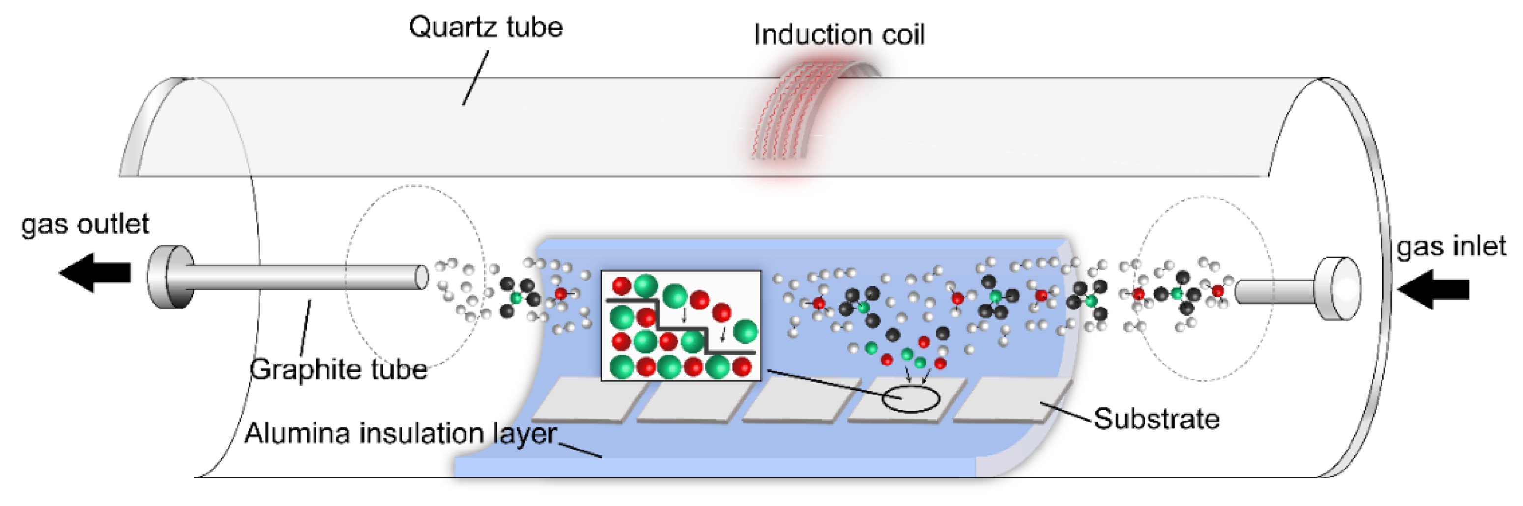
Figure 1 illustrates a schematic diagram of the CVD apparatus. The reaction chamber was nested with a cylindrical quartz tube to form a vacuum atmosphere, an alumina cylindrical block as a heat insulator, and a graphite tube (
L = 400 mm,
Φout = 50 mm,
Φint = 40 mm) to heat the reaction zone and substrate by high-frequency induction coils outside the quartz tube. The high-frequency coil was powered by an induction heating power supply (CYP-50), the frequency of which was 30–50 kHz. Entering the chamber, the reaction raw materials (CH
4 and SiCl
4) absorbed energy to decompose and generate intermediate reactants (HCl, SiCl, Cl, etc.). Then, part of the reactant molecules and intermediate reactants gradually diffused and adsorbed on the surface of the substrate, which chemically reacted on the surface of the substrate and formed a thin film. Finally, unreacted species and by-product molecules diffused outward and were recovered.
The repeatability limitation of CVD technology often comes from the need for a high vacuum. The substrate should be placed in the chamber immediately after cleaning to avoid contact with the fibers. The gas flow rate should be slowly increased by a gradient to avoid changes in the substrate position. Contamination of the chamber caused by residual precursors often greatly affects the vacuum level. So, the use of replaceable quartz tubes and frequent cleaning of sealing items such as valves and rubber rings are recommended for films synthesis. In addition, a cold trap device was connected to the chamber outlet for processing by-products to keep the chamber clean.
SiCl4 (99.5% purity; Aladdin, Shanghai, China) and CH4 (99.999% purity; Xiangyun Industry, Wuhan, China) were used as silicon and carbon sources, respectively. The SiCl4 was heated to 353 K by an evaporation device and mixed with H2 and CH4. The flow rates of the precursors were regulated by flow controllers (MFC; Sevenstar, Beijing, China). The mixed gas was transported into the vacuum chamber through a graphite tube (L = 270 mm, Φout = 15 mm, and Φint = 10 mm). The flow rate of the H2 and SiCl4 was set at 4000 and 66 sccm, respectively. The flow rate of the CH4 was set at 53, 66, and 86 sccm, which made RC/Si = 0.7, 1.0, and 1.3, respectively. The silicon carbide was deposited on the 4H-SiC single crystalline substrates (4.0° toward <11–20>; Tianyue Industry, Shandong, China) for 5 min with the pressure being stably controlled at 5 kPa. Ultimately, the by-product was treated via a purification device filled with activated carbon and sodium hydroxide spray scrubber.
Iftekhar Chowdhury et al. prepared 4H-SiC by hot-wall CVD on SiC substrates with a growth rate of 15 μm/h at 1823 K, and evidence of the significant formation of silicon droplets and comet-like inclusions was observed [
16]. After the silicon source gas was replaced from silane with dichlorosilane, the deposition rate reached 50–75 μm/h at 1923 K. L. Yang et al. prepared 4H-SiC on 4H-SiC substrates. As the temperature increased from 1823 to 1923 K, the conversion rate of basal plane dislocations (BPDs) to threading edge dislocations (TEDs) decreased, leading to the suppression of lateral growth. Accordingly, the experimental temperature range was designed from 1773 K to 1973 K [
17]. The temperature distribution measured by thermocouple from inlet to outlet is shown in
Figure 2. At the center of the graphite tube, the temperature reached the highest level, but was about 23 K lower than the preset ones. The deposition temperature (
Tdep) in the graphite tube decreased gradually from the center to the two ends. Based on the temperature distribution, five substrates were placed in the graphite tube from the center to the outlet at every interval of 50 K in order to obtain multiple samples at different conditions simultaneously, i.e., a kind of high-throughput synthesis. Specifically, the temperature was controlled under the preset temperature of 1973 K, and the substrates were placed at the position of A, B, C, D, E in
Figure 2, respectively, so that the temperature difference between adjacent substrates was 50 K. In addition, the substrates were placed at
Tdep = 1750 K, at the positions of E, F, and G under the preset temperatures of 1973, 1873, and 1773 K, respectively, to research the effect of position.
Figure 3 shows the contour of the gases’ velocity inside the graphite tube simulated by Gambit software. The gas velocity reaches the maximum at the center of the cylindrical tube and gradually decreases toward the tube wall. The gas experiences turbulent flow at the cylindric center, but stable static flow at the half of the radial direction. In addition, the gas velocity at the outlet area is more complex than that at the inlet area. Therefore, the substrates for deposition were placed on a graphite plate at the half of the radial direction to keep a steady gas flow, which is beneficial to the epitaxial growth of thin films [
18].
Figure 4 reveals the contours of the mass fraction of gaseous raw materials (CH
4, SiCl
4 and H
2) in the chamber. It can be seen from
Figure 4b that the hydrogen was evenly distributed in the chamber during the experiment. In
Figure 4a, in the central area of the chamber, the distribution of gas materials was relatively uniform. As the distance gradually approached the outlet area, the distribution of gas raw materials became gradually uneven, and the phenomenon of gas accumulation occurred.
The crystalline phases and preferred orientation were analyzed by X-ray diffraction (θ–2θ) with Cu-Kα radiation (XRD, 40 kV, 40 mA and 4°/min, Ultima III; Rigaku, Tokyo, Japan). The surface and fracture morphologies of the thin films were observed using a 20 kV field-emission scanning electron microscope (Quanta-250, FEI, Houston, TX, USA). The deposition rate (Rdep) was calculated from the thickness of the thin films and experimental time. A Raman spectrometer (LabRAM HR Evolution; Horiba, Paris, France) was used for Raman spectra measurements excited by a 532 nm wavelength diode laser.
3. Results and Discussion
The detection depth of Raman spectra is much lower than that of XRD, which is better to omit the influence of 4H-SiC substrate.
Figure 5 shows the Raman spectra of the thin films prepared at 1750 to 1950 K under the preset temperature of 1973 K. According to the standard spectra of SiC, the E
2(TO) of 4H-SiC is the characteristic peak to distinguish 3C-SiC; furthermore, the relative strength of the A
1 (LO) band of 4H-SiC is lower than that of the LO band of 3C-SiC [
19,
20]. At 1750 and 1800 K, only 4H-SiC was formed, while 3C- and 4H-SiC mixtures were formed at 1850 K. Graphite was identified at levels higher than 1900 K. The anomalous behavior at 100–200 cm
−1 was typical of the Raman spectrum of amorphous SiC, indicating mixed features of amorphous/distorted and crystalline silicon carbide [
21,
22]. According to the Raman spectra, the crystalline phases of the thin films prepared at different temperatures and
RC/Si are summarized in
Figure 6. The boundaries of the different crystalline phases regions are determined by the numerical values of the process parameters of the preparation, and the median value is taken as the endpoint. The 4H-SiC, 3C-SiC and C only appeared at
Tdep = 1750 K,
RC/Si = 1.3.
In SiC crystals, defects may hinder the propagation of phonons [
23]. When the Raman scattering laser irradiates the SiC crystal, the photons collide with each other in the lattice, resulting in a shorter phonon lifetime. The more defects, the shorter the lifetime of the phonons, which ultimately makes the FWHM of the LOPC mode gradually become wider in the Raman spectrum [
23,
24]. Therefore, the FWHM of the Raman peak is possible to reflect the quality of the SiC crystal.
Figure 7 reveals the FWHM of the LO peak in the Raman spectra of the SiC film grown at different deposition temperatures and
RC/Si. The FWHMs increased slightly with increasing temperature from 1750 to 1800 K, and then decreased to the lowest point at about 10 cm
−1 at temperatures higher than 1850 K. In another word, the SiC crystal may have the highest quality at 1850 K.
Figure 8 reveals the XRD patterns of the grown SiC films to reflect their preferred orientation. Due to the 4H-SiC single crystalline substrate with 4.0° tilted toward <110> being applied in this study, no characteristic peak of the substrate was identified. Combined with the results of Raman spectra in
Figure 5, the (004)-oriented 4H-SiC was grown at levels lower than 1850 K; non-oriented 3C-SiC was co-deposited with graphite at levels higher than 1900 K. The relative intensity of the C characteristic peak at 26° was much larger than that of the 3C-SiC characteristic peak in
Figure 8i,j, and the relative intensity of the 4H-SiC characteristic peak at 35.6° was much larger than that of the 3C-SiC characteristic peak in
Figure 8o, so the ordinates were processed, resulting in lots of noise in the XRD. In addition, in
Figure 8k, the relative intensity of the characteristic peaks of 4H-SiC was relatively low, and the dispersion peak was more obvious around 27° owing to the amorphous components presented in the film, resulting in a slanted pattern. Since the volume or weight of a substance participating in diffraction is proportional to its diffraction intensity, the relative ratio of each phase can be calculated from the ratio of the peak area when the diffraction intensity of each XRD characteristic peak is not much different.
The orientations of the SiC films were evaluated by the Lotgering factor (
Fhkl) by Equation (1).
Phkl and
P0 are the ratios of the peak intensities of the (hkl) planes and the sum of all peaks for the films (
Phkl) and powders (
P0), respectively. The
Fhkl value of 1 indicates that the sample has a completely preferred orientation. The
Fhkl of 0 indicates that the samples and the powders have the same diffraction peaks, indicating non-orientation [
25].
Figure 9 presents the FWHMs and the
F004 of the 4H-SiC (004) at the C/Si ratio of 1.3, The FWHM decreased and then rose slightly with increasing
Tdep, showing the lowest value of 0.15 at 1850 K, indicating the highest crystallinity at 1850 K. As the temperature increased, the
F004 was close to 1.0 at 1750 to 1850 K and then decreased to 0.52 at 1950 K, indicating the (004)-orientation became weak.
Figure 10 reveals the pole figure of the 4H-SiC substrate with a 4.0° off-angle and the SiC film at 1823 K and
RC/Si = 1.3. The deposited thin film was 4H-SiC. The diffraction peaks appear once every 60°, indicating a hexagonal symmetry. Moreover, there is a slight deviation (about 5°) in the azimuth angle of the diffraction pole between the substrate and the deposited film, which corresponds to the off-angle of the substrate.
Figure 11 demonstrates the surface morphologies of the thin films at different temperatures and
RC/Si. At 1750 K, the surface microstructure is smooth, and the grain size is about 100 nm; at 1850 K, some hollows are observed, which may be etched by hydrogen; at 1950 K, many grains were formed on the surface. With increasing temperature, the surface roughness increased, and some large grains were observed on the surface.
Figure 12 shows the fracture morphology of the thin films prepared at different temperatures and
RC/Si. The dense cross-sectional microstructure is observed at
Tdep = 1750 and 1850 K, while some lamella microstructures were observed at 1950 K, e.g.,
Figure 12c, which is graphite combined with the results of EDS spectra, Raman spectra, and XRD patterns. The deposition rate was calculated by the cross-sectional thickness dividing the deposition time, as shown in
Figure 13.
Figure 13 shows the effect of deposition temperature on the deposition rate of the SiC films under different conditions, which is between 30 and 185 μm/h. At
RC/Si = 0.7 and 1.0, the deposition rate increased with increasing deposition temperature and then decreased gradually, showing the maximum at around 1873 K, while at
RC/Si = 1.3, the deposition rate decreased in the range of 1773 to 1823 K and then had the same tendency. In addition, with the increase in the C/Si ratio from 0.7 to 1.3, the deposition rate gradually decreased. The source gas cannot obtain enough energy to decompose at low
Tdep, so the number of active groups is insufficient, resulting in the low
Rdep. In addition, the movement speed of gas-phase particles in the chamber is slow, and active atomic clusters cannot quickly diffuse to the surface of the substrate for effective adsorption at low
Tdep, so it is difficult to form a crystal nucleus [
26,
27], resulting in a decrease in the deposition rate. As the deposition temperature increases, the source gas obtains enough energy to generate more active atomic clusters. In addition, the increase in temperature also makes the activity of gas molecules more intense, and the diffusion rate of active atomic clusters increases, indicating that the active atomic groups can quickly diffuse to the surface of the substrate. The migration rate of active atoms on the surface will also increase, which will rapidly gather to the formed crystal nucleus, leading to an increase in the deposition rate. When the temperature rises to a certain level, it can be seen from the Raman spectra that the methane raw material begins to decompose into deposited carbon in large quantities, resulting in a decrease in the deposition rate.
To research the influence of the substrate position on the growth of SiC films, the films were grown at
Tdep = 1750 K and
RC/Si = 1.3, at the positions of E, F, and G in
Figure 2, i.e., 100, 130, and 200 mm under the preset temperature of 1973, 1873 and 1773 K, respectively.
Figure 14a demonstrates the Raman spectra of the films prepared at different positions. All the films prepared at the same temperature but different positions were 4H-SiC.
Figure 14b shows the XRD patterns of the 4H-SiC films prepared at the same temperature but at different positions. All the films were highly (004)-oriented 4H-SiC, while the FWHM of the (004) peak at 200 and 130 mm is much lower than that at 100 nm, indicating the highest crystallinity. The surface and fracture morphologies of the SiC films reveal that as the position approached the outlet, the surface roughness and the grain size gradually increased, whereas the deposition rate (thickness) decreased. This indicates the precursor of SiCl
4 may be consumed from the center to the outlet, forming a precursor’s concentration gradient, which is consistent with FWHM in the XRD patterns. Therefore, the distribution of gaseous materials in the chamber has less influence on the preparation process than temperature. The film is of high quality and high crystallinity in the central area where the gas raw materials are evenly distributed.


 ,
, 