Article

Effect of Annealing Temperature on the Microstructure and Optical Properties of Lanthanum-Doped Hafnium Oxide

1
Xinjiang Key Laboratory of Solid State Physics and Devices, Xinjiang University, Urumqi 830046, China
2
School of Physics Science and Technology, Xinjiang University, Urumqi 830046, China
*
Author to whom correspondence should be addressed.
Coatings 2022, 12(4), 439; https://doi.org/10.3390/coatings12040439
Submission received: 15 February 2022 / Revised: 13 March 2022 / Accepted: 18 March 2022 / Published: 24 March 2022

Abstract

:
Lanthanum-doped HfO2 films were deposited on Si by sol–gel technology. The effects of annealing temperature on the optical properties, interface chemistry, and energy band structure of Lanthanum-doped HfO2 films have been investigated. The crystallinity and surface morphologies of the films are strongly dependent on the annealing temperature. X-ray diffraction (XRD) analysis showed a monoclinic phase, and there was a tendency to preferentially grow with increasing temperature. The calculated grain sizes ranged from 17.1 to 22.4 nm on average. It was also confirmed from Raman spectroscopy that increasing the annealing temperature can improve the crystallinity of the films. The surface of the film was smooth, and the film had good interfacial contact with the silicon substrate. The band gap increased from 5.53 to 5.91 eV with increasing annealing temperature. The calculated conduction band offset and valence band offset both exceeded 1 eV. In conclusion, smaller grain size, good crystallinity and interfacial contact can be obtained by adjusting the annealing temperature. Higher conduction band and valence band offsets can meet the minimum barrier height requirements of complementary metal oxide semiconductors (CMOS) and have potential applications.

1. Introduction

In order for the metal-oxide-semiconductor field-effect transistor (MOSFET) to be fully utilized in integrated circuits, the feature size of semiconductors has to be continuously reduced. It is particularly important to reduce the size of the gate dielectric layer. The quantum tunneling effect causes an exponential rise in gate leakage current with decreasing feature size, which seriously affects the stability and reliability of the device. The traditional SiO2 gate dielectric material can no longer match the actual demands, and the use of high dielectric constant (high-k) materials to replace SiO2 as the gate dielectric of CMOS transistors has become the focus of research [1,2,3,4]. In this paper, HfO2 is selected to replace the traditional SiO2 gate dielectric material, and the aforesaid issues can be effectively addressed by reducing the thickness of the gate material and increasing the width of the band gap.
The HfO2 gate dielectric film has a high dielectric constant (k ~ 25) [5], a relatively large band gap (~5.8 eV) [6,7,8,9,10], excellent thermal stability, stable chemical properties, and a suitable conduction band deviation from the Si substrate. It has received widespread attention and has become an ideal candidate material to replace the traditional SiO2 gate dielectric. When it is combined with a metal gate material with a lower work function, a higher potential barrier can be obtained, and thus a smaller leakage current can be obtained. The HfO2 material does not react with the silicon substrate at high temperatures and maintains good stability. However, HfO2 gate dielectrics still have some drawbacks. The polycrystalline structure starts to appear under annealing conditions at 450 °C. The generation of grain boundaries can provide channels for leakage currents and can produce low-k interface layers, and the generation of interfacial defects can also reduce the carrier mobility.
HfO2 gate dielectric material modification can significantly increase its performance. Because ZrO2 and HfO2 have similar crystal structures and lattice constants, causing lattice defects is difficult. Ahn et al. [11]. prepared a high gate dielectric film doped with 3% Si to Zr0.4Hf0.6O2 by atomic layer deposition (ALD). Annealing at 600 °C for 2 min in N2 atmosphere can obtain a stable cubic phase with a dielectric constant of about 50. Zr-rich Zr1-xHfxO2 films require less Si doping than Hf-rich films when transformed into tetragonal structures. It is demonstrated that in single metal oxides, the phase transition of Hf requires more Gibbs free energy than Zr. Chiang et al. [12] found that ZrO2 doping not only reduced the effective oxide thickness (EOT) of Hf0.2Zr0.8O2 film but also increased the device time-to-failure (TTF) by three orders of magnitude. On the other hand, the leakage current of the Hf0.2Zr0.8O2 gate dielectric film is two orders of magnitude higher than the HfO2 sample. The reason is that ZrO2 has a lower band gap width than HfO2, and generates ZrSiOx at the interface. Ye et al. [13]. doped 21 at.% of TiO2 with HfO2 and annealed at 500 °C to prepare HfTiO film with a dielectric constant of 44. The results reveal a decrease in the leakage current, which is mostly due to an improvement in the film microstructure. According to Liang et al. [14], Y-doped HfO2 thin film may achieve a stable cubic phase, reduce the crystallization temperature and increase the prohibited band width of the film. The HYO/Si gate stack had better interface properties. Gd2O3 doped HfO2 film can inhibit the capture and release of electrons, increase device reliability, and reduce leakage current. The study of Ma et al. [15] showed that the introduction of Gd through heat treatment can effectively improve the C–V characteristics of the samples and effectively increase the dielectric constant. In addition, SiO2 or silicate often exists between the thin film and the Si substrate, and these substances will impact the condition of the thin film interface layer. The presence of SiO2 reduces the interfacial contact and reduces the equivalent oxide thickness. The annealing process can promote silicide to silicate conversion. The addition of silicate can significantly increase the electrical characteristics of thin film materials. Tang et al. [16]. injected strontium into HfO2, and by increasing the Sr content and film thickness, the film was converted from a monoclinic to a cubic phase, with an enhanced dielectric constant. The ferroelectricity of HfO2 films can be controlled by doping and mechanical stress.
Different elements can be doped to improve the physical and chemical characteristics of HfO2 film. However, there are also problems such as reduced dielectric constant and increased leakage current. With a large band gap (~5.5 eV) and high dielectric constant (k ~ 30), La2O3 has been shown to exhibit good thermodynamic and electrical properties in CMOS devices [6,17]. Nonetheless, there are few studies on the preparation of La2O3 by sol–gel method. There are many techniques for preparing HfO2 thin films, including sol–gel method [18,19], chemical vapor deposition (CVD) [20], molecular beam epitaxy (MBE) [21], pulsed laser deposition (PLD) [22] and atomic layer deposition [23,24]. Compared with the above preparation techniques, the sol–gel method is simpler in operation, lower in cost, and easy to control the material composition, which is conducive to large-scale commercial production [25,26,27,28,29,30,31].
In this study, lanthanum-doped HfO2 thin films were deposited on Si substrates by the sol–gel technique. The aim is to systematically study the optical characteristics, interfacial chemistry and band structure changes caused by annealing temperature systematically. By adjusting the annealing temperature, the grain size and thin film densification can be reduced to meet the requirement of MOSFET feature size reduction. Increasing the forbidden band width enables the conduction and valence band offset of the sample to meet the requirement of the barrier height. Increasing the crystallization temperature expands the application of the gate dielectric material.

2. Materials and Methods

2.1. Materials

The P-type silicon (100) substrate was provided by Zhejiang Lijing Silicon Materials Co., Ltd., (Zhejiang, China). Acetone was produced by Sinopharm Chemical Reagent Co., Ltd., (analytical grade, 99.5%, Shanghai, China) ethanol was from Tianjin Xinbote Chemical Co., Ltd., (analytical grade, 99.7%, Tianjin, China). Ammonium hydroxide solution (NH3•H2O) was provided by Aladdin (analytical grade, 28%, Shanghai, China). Hydrogen peroxide solution (H2O2) was provided by Aladdin (analytical grade, 30 wt% in H2O, Shanghai, China). Hydrofluoric acid was produced by Tianjin Xinbote Chemical Co., Ltd. (analytical purity, 40%, Tianjin, China). Hafnium chloride (HfCl4) was provided by Aladdin (analytical grade, 99.5%, Shanghai, China). Lanthanum nitrate hexahydrate (La(NO3)3•6H2O) was produced by Aladdin (analytical grade, 99.99%, Shanghai, China).

2.2. Preparation

In the current work, a p-type Si (100) single-sided polished wafer with a resistivity of 1–20 Ω cm was selected as the substrate. First, it was ultrasonically cleaned with acetone and absolute ethanol for 10 min, and then a mixed solution (NH3•H2O:H2O2:H2O = 2:1:7) was used to remove organic matter and impurity ions. Then the diluted hydrofluoric acid solution was used to clean the silicon wafer to remove the oxides naturally formed on the surface. During the entire cleaning process, deionized water was used to clean the reagents used. It was set aside after drying. In this work, HfCl4 and La(NO3)3•6H2O were used as precursors, which were prepared by dissolving in ethanol and adding an appropriate amount of deionized water. The concentration of the solution was 0.05 M. The doping amount of La was 5% of Hf. It was stirred vigorously for 2 h and left for a while. It was filtered with a 0.2 μm PTFE membrane injection filter, spin-coated at a speed of 3000 rpm for 30 s, and heated on a heating table (HP-1515, Wenzhou Hanbang Electronics, Zhejiang, China) at 150 °C for 5 min to cure the film and remove excess solvent. The samples were annealed at 400, 500, 600, and 700 °C for 1 h using a vacuum tube high-temperature sintering furnace (OTF-1200X, Hefei Kejing Material Technology, Heifei, China).

2.3. Characterization

X-ray diffraction (XRD, Bruker, Karlsruhe, Germany) was used to obtain the compositional structure and crystalline state of the films in the sweep range of 20–60° with Cu Kα. The functional groups of the films were obtained using Fourier transform infrared spectroscopy (FTIR, Bruker, Karlsruhe, Germany). Raman spectroscopy (Raman, LabRAM HR Evolution, HORIBA Scientific, Paris, France) was used to characterize the state of the films. The surface morphology and thickness of the film were characterized by the secondary electron signal of scanning electron microscope (SEM, SU8020, Hitachi, Japan). X-ray photoelectron spectroscopy (XPS, ESCALAB 250Xi, Thermo Fisher, Waltham, IL, USA) was used to characterize the chemical bond state of the sample film. A UV-Vis spectrophotometer (UV-Vis, Lambda 650S, PerkinElmer, Norwalk, CT, USA) was used to measure the transmission spectrum of the thin film deposited on the quartz substrate and calculate the optical band gap.

3. Results and Discussion

3.1. Structure Analysis

The XRD profiles of lanthanum-doped HfO2 films deposited on silicon substrates at various annealing temperatures are presented in Figure 1. After annealing at below 500 °C for one hour, no obvious diffraction peaks were detected, which indicates that at a relatively low temperature, the annealed film is still in an amorphous state. This is consistent with the result of Jin et al. [26]. As the temperature increased at 600 °C, obvious diffraction peaks appeared, and all peaks corresponded to the monoclinic phase structure of HfO2 compared with the standard card. The phase transition of the film occurred at 600 °C. The diffraction peaks at 700 °C were compared with the standard card, and it was found that all peak positions corresponded to the monoclinic structure of HfO2. By comparing with the standard card PDF#73-0445 of La2Hf2O7, it was found that the corresponding peak appeared at 600 °C. The XRD analysis shows that with the increase in temperature, the diffraction peak position of the sample obviously moves to a small angle, revealing the existence of tensile stress inside the sample. The crystallite size was calculated using the Debye–Scherrer formula [32,33,34]:
D = K · λ β · cos θ
where D is the grain size, K is the Scherrer constant, β is the full-width at half maximum (FWHM), λ is the X-ray wavelength, and θ is the diffraction angle. For the films annealed at 600 °C, the diffraction peaks were obvious, and the calculated average grain size was 21.1–22.4 nm. Among them, (−111) crystal plane was 21.1 nm; (111) was 22.4 nm. With the increase in the annealing temperature, the intensity of the diffraction peak at (−111) of the film annealed at 700 °C increased, which improved the crystallinity of the film. This resulted in stronger and narrower diffraction peaks, a decrease in full width at half maximum, and an increase in the grain size at the (−111) plane to 21.9 nm. The average grain size was 17.1–21.9 nm. The increase in the intensity of diffraction peaks was caused by the preferred orientation, which made the grains with different orientations converge to the same spatial orientation. As a result, the intensity of some diffraction peaks in the XRD image was reduced or could not be obtained.

3.2. Bonding Structure Analysis

The Fourier transform infrared (FTIR) spectra of the thin film samples prepared at different annealing states are shown in Figure 2. In all the thin film samples, absorption peaks located in the low wave number region appeared at 424, 512, 564 cm−1 associated with Hf–O chemical bonding [35]. Meanwhile, a broad peak existed between 700 and 750 cm−1, and a vibrational peak about HfO2 was formed at 739 cm−1. In addition, due to the existence of the silicon substrate, there was a strong vibration mode at 610 cm−1 in the FTIR spectra of all thin film samples. In addition, the C–O vibration mode was also detected in the spectrum, located at 670 and 1732 cm−1 in the spectrum, respectively. It can be directly observed that the peak intensity of the vibration mode at 1732 cm−1 gradually increased with the increase in temperature. At the same time, the Si–O vibration mode was also detected in the spectrum, which was located at 890 and 1108 cm−1 in the spectrum [36]. The vibration mode at 1108 cm−1 was wider and the peak intensity was larger, which may have been caused by the optical stretching of Si–O in the transverse direction. Similarly, the vibrational mode of hafnium silicate (Si–O–Hf) was present in the spectrum at 820 cm−1 and was shifted toward the lower wave number with increasing temperature [37]. The existence of Si–O–Hf and Si–O vibration modes was found in the spectrum inspection, which may have been due to the formation of good contact between the film and the Si substrate, and the formation of silicate at the interface layer. This can be seen in the cross-sectional view of the thin film sample from the SEM, where the thin film has strong contact with the substrate. Additionally, a vibrational mode associated with HfSiOx at 970 cm−1 was present in the FTIR spectrum. In addition, a vibrational mode of La–O at 471 cm−1 was detected in the low wave number region.

3.3. Raman Spectra Analysis

Raman spectroscopy was used to analyze the microstructure of samples in the deposited state and in different annealed states of HfO2 films doped with 5% lanthanum. Raman spectroscopy effectively analyzed the optical phonon modes present in the samples by molecular vibration characteristics. In the theoretical prediction, there were 36 phonon modes in total for the estimated statistics of monoclinic HfO2, including 18 Raman-active modes (9Ag + 9Bg), 15 IR-active modes (8Au + 7Bu), and three zero-frequency translation modes. For tetragonal HfO2, there were three IR-active modes (A2u + 2Eu) and 3 Raman-active modes (A1g, B1g and Eg). Relatively few were cubic phase HfO2, which has only one IR-active mode (F1u) and one Raman-active mode (F2g) [38]. As can be seen in Figure 3, there was an intense Si body phonon signal at 525 cm−1, which should be attributed to the amorphous state of the Si substrate [35]. A Raman signal about the Si substrate was present at 438 cm−1. It is also seen that the intensity of the peaks at 348, 624, and 676 cm−1 rose with increasing annealing temperature, indicating that the crystallinity of the films increases with increasing annealing temperature, which corresponds with the XRD pattern [37]. Both of the characteristic signals at 348 and 624 cm−1 belong to the two Ag phonon modes. The discovery of HfO2 signals was also able to confirm the crystallization of the film samples at conditions higher than 500 °C. There was a wider Raman signal at 830 cm−1, which was confirmed to be a Bg phonon mode after comparison [39]. When the aforesaid Raman signal analysis was combined, it was inferred that the produced film sample was monoclinic HfO2.

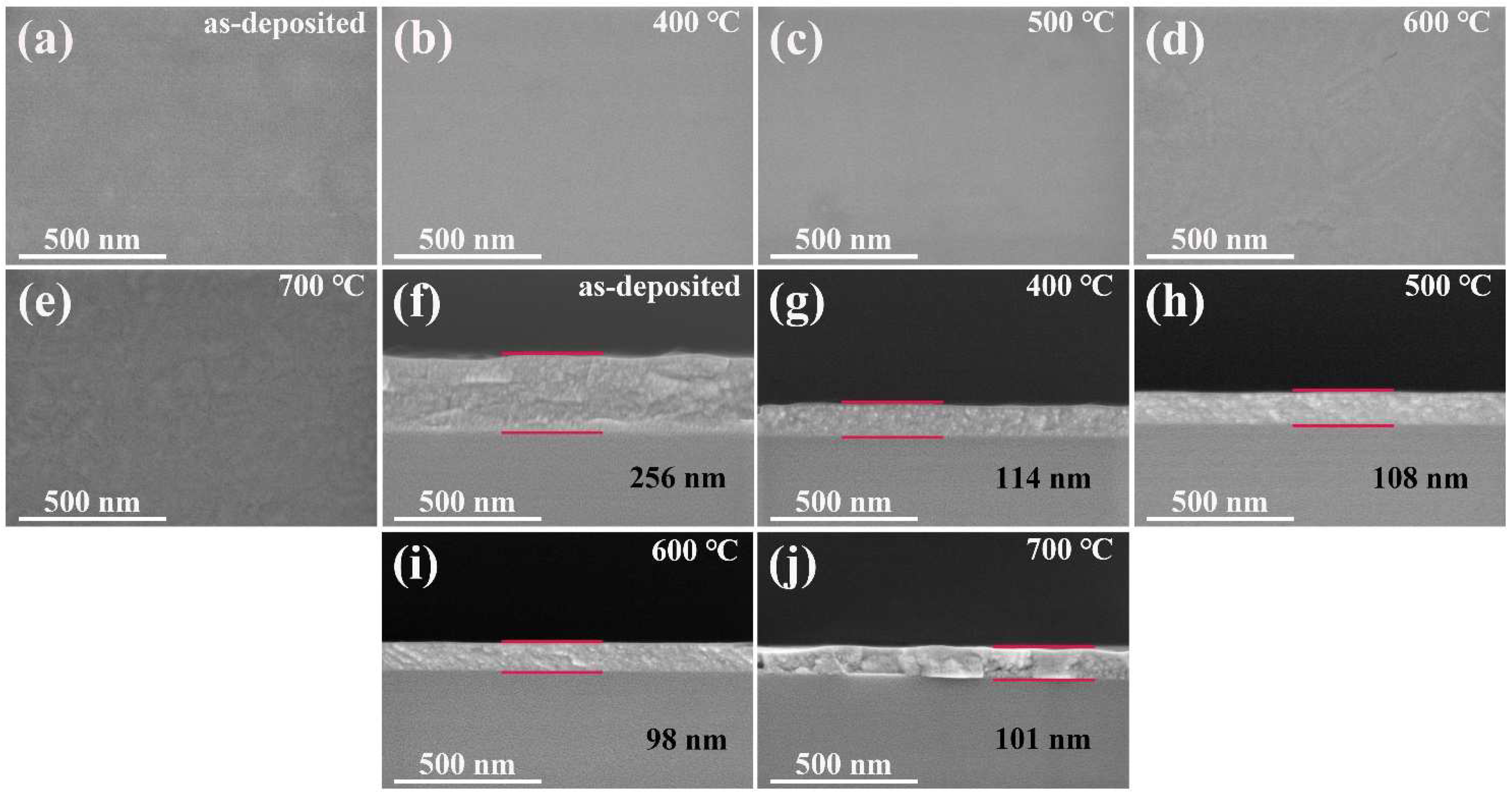
3.4. Morphology Analysis

The surface and cross-sections of the thin film samples were characterized by scanning electron microscopy. Figure 4a–e shows the surface morphology of lanthanum-doped HfO2 thin films at various annealing temperatures. It can be seen from the figure that the surface of the film is smooth, and no surface defects such as cracks or pores. Some patterns are found in Figure 4d,e. The appearance of the pattern is caused by the crystallization of the film. After the film crystallizes, it grows toward a more densified state. Figure 4f–j depicts the topographical states of the film interface. It is evident that as the annealing temperature is raised, the film thickness drops from 256 to 98 nm. After annealing at 400 °C, the large reduction in film thickness was caused by the conversion of oxyhydroxide inside the film to oxide and the densification after high temperature annealing. The film thickness increases at 700 °C compared to 600 °C, which corresponds to the results of the XRD patterns. This is owing to preferentially orientated grain development and grain size increase at 700 °C. Simultaneously, the figure shows that the film and the substrate are tightly bonded and have good interfacial contact.

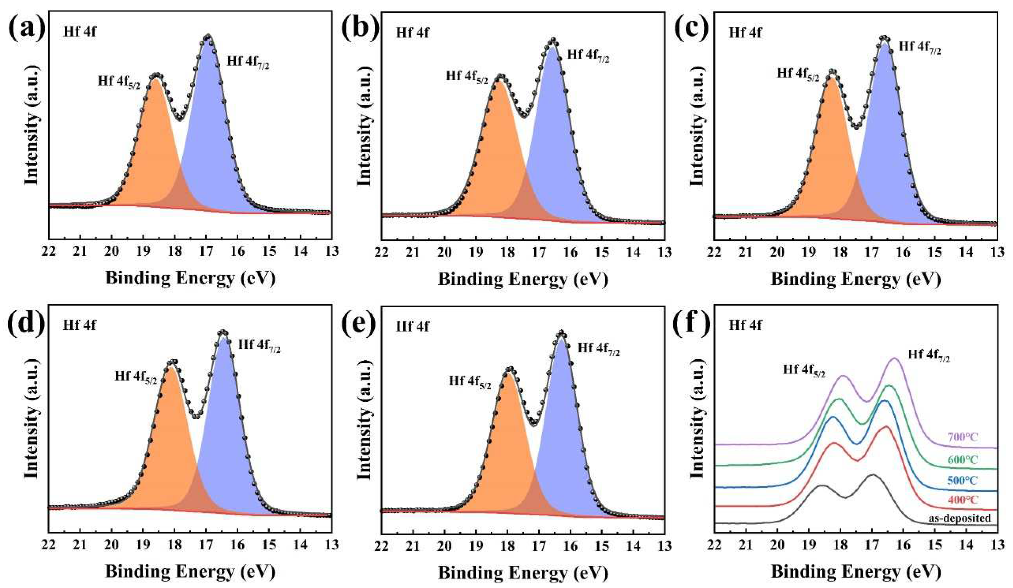
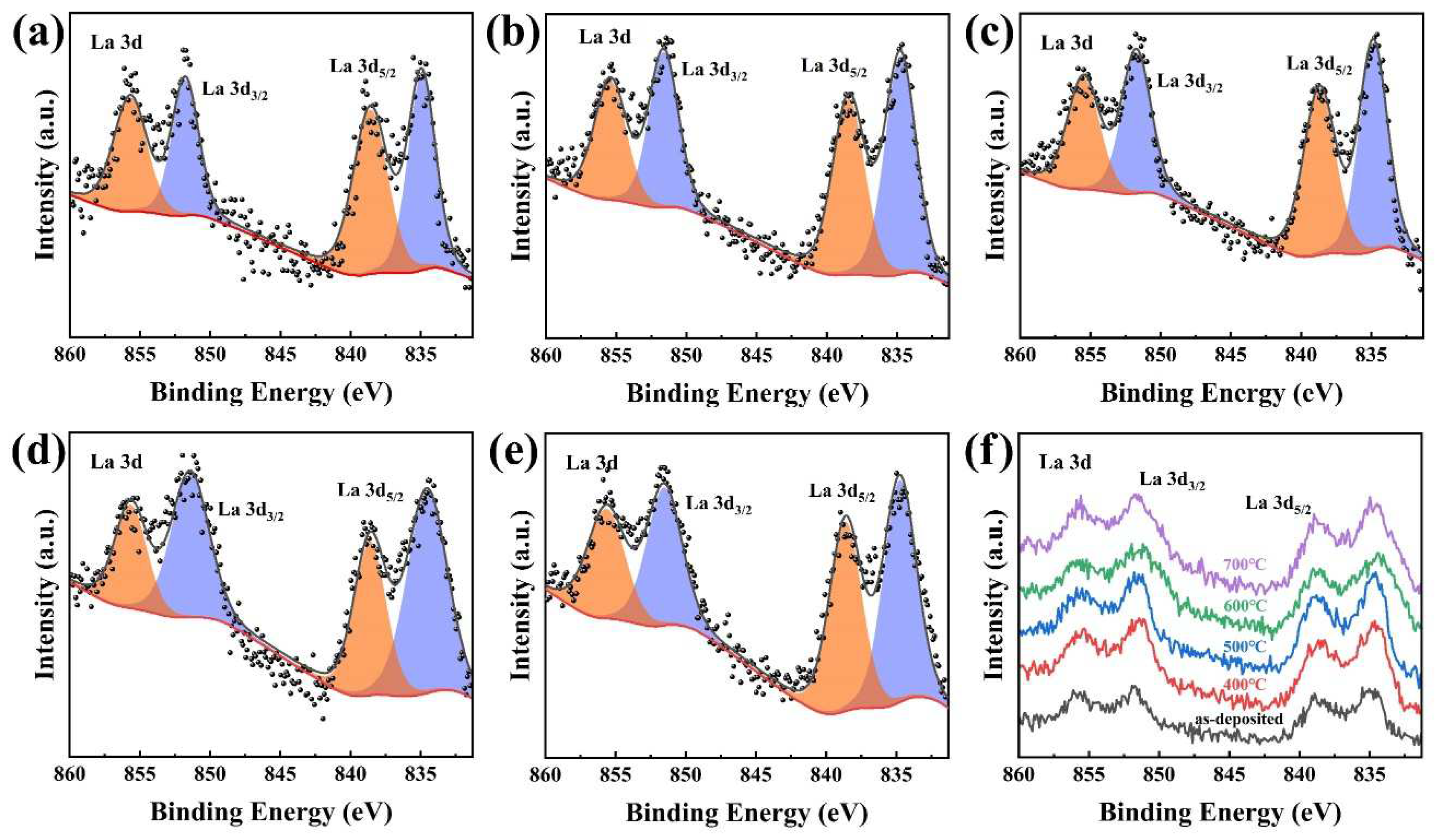
3.5. Chemical Compositions and States

The interfacial chemical states of the lanthanum-doped HfO2 films were investigated by XPS tests at different annealing temperatures, and the sample chemical states were studied by fitting the plots to the corresponding Gaussian and Lorentzian functions. The full XPS spectrum in Figure 5 shows that the elements detected in the sample are the presence of Hf, La, O and C. The measurement spectrum analysis of all elements is first calibrated by the binding energy of the C1s peak (284.8 eV). The presence of carbon in the complete spectrum can be ascribed to the sample being exposed to the air environment throughout the experimental and test phases, causing some carbon to be adsorbed on the surface of the film.
We analyzed the O 1s peak of the XPS spectrum of the lanthanum-doped HfO2 film, and obtained the sub-peaks in Figure 6 below after fitting. They were mainly divided into 529.9 eV metal-oxygen (M–O) bond, 531.0 eV oxygen vacancy (Vo), and 531.4 eV surface oxygen (M–OH) bond, which is in good agreement with Zhang’s data [40]. When comparing Figure 6a,b, it is obvious that the surface oxygen (M–OH) bond was greatly diminished following annealing treatment. At the same time, the M–O bond greatly increased. This suggests that after annealing, the majority of the surface oxygen is coupled with metal cations to create new bonds. Under the effect of annealing conditions, lanthanum is doped into HfO2, and substitutional doping causes distortion of the crystal lattice. At the same time, the oxygen vacancy decreases, which increases the coordination number of the metal, and the oxygen atom combines with the metal atom to form an M–O bond. As seen in these figures, compared with the film annealed at 400 °C (M–O: 66.6%, Vo: 21.8%, M–OH: 11.6%), the film annealed at 700 °C (M–O: 77.9%, Vo: 8.8%, M–OH: 13.3%) had more M–O bonds and fewer oxygen vacancies. Therefore, an increase in the annealing temperature can suppress the generation of oxygen vacancies. The fitted O 1s peaks move in the direction of high binding energy when the crystallization temperature is used as a boundary, both before and after crystallization. This is due to an increase in M–OH bonds and a decrease in oxygen vacancies. The shift will be caused by crystallization changing the local bond energy.
Figure 7 show the XPS spectra of Hf 4f of lanthanum-doped HfO2 films at different annealing temperatures. The Hf 4f core energy levels of all samples are deconvoluted into two Gaussian peaks as Hf 4f5/2 and Hf 4f7/2. The spin-orbit doublet is 1.68 eV, which is consistent with the reference data [41,42]. At the same time, no harmful Hf-Si bond formation was found at the lower binding energy. Compared with the spectrum of Hf 4f in the as-deposited state, the introduction of annealing temperature causes the peak intensity to become larger. At the same time, as the annealing temperature increases in Figure 7f, the Hf 4f peak of the sample shifts slightly to the direction of lower energy, which may be attributed to the change in the chemical state of the element caused by the doping of La. Figure 8 shows the La 3d patterns found in the XPS test. Due to the low content of the La element, the image quality is poor, but it can also be clearly detected that the core energy levels of La 3d are deconvoluted into La 3d3/2 and La 3d5/2. The La 3d peak has no obvious shift change.
Table 1 shows the proportion of each element of the film at each annealing temperature by XPS spectroscopy. In the as-deposited state, the atomic ratio of oxygen to hafnium (O/Hf) is 3.31. The reason is that the composition of the film is mainly hafnium oxyhydroxide (HfO(OH)2) at low temperatures. At the same time, the presence of partial Si–O bonds leads to a relative increase in oxygen element, which can be obtained from the FTIR phase. As the annealing temperature increases, the value of O/Hf decreases to 2.5. This indicates the gradual transformation of oxyhydroxides to oxides, which can also be obtained from the O 1s XPS spectral analysis.

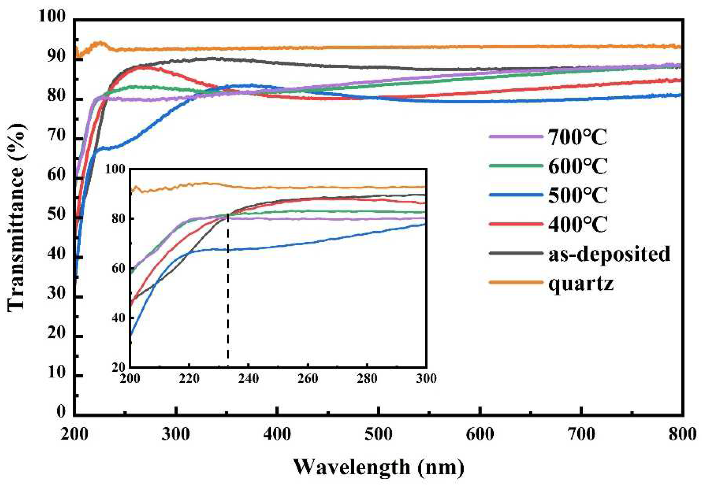
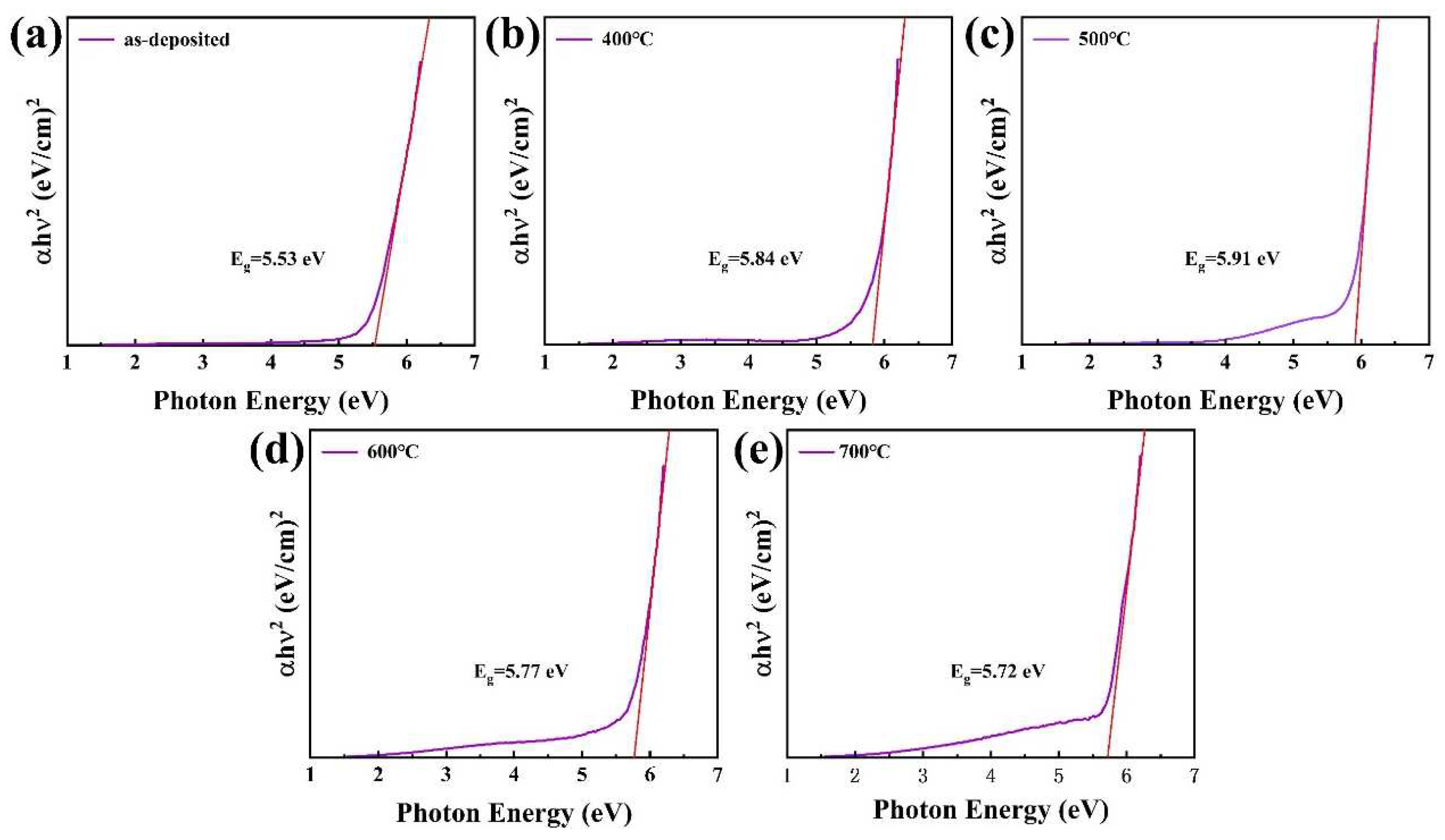
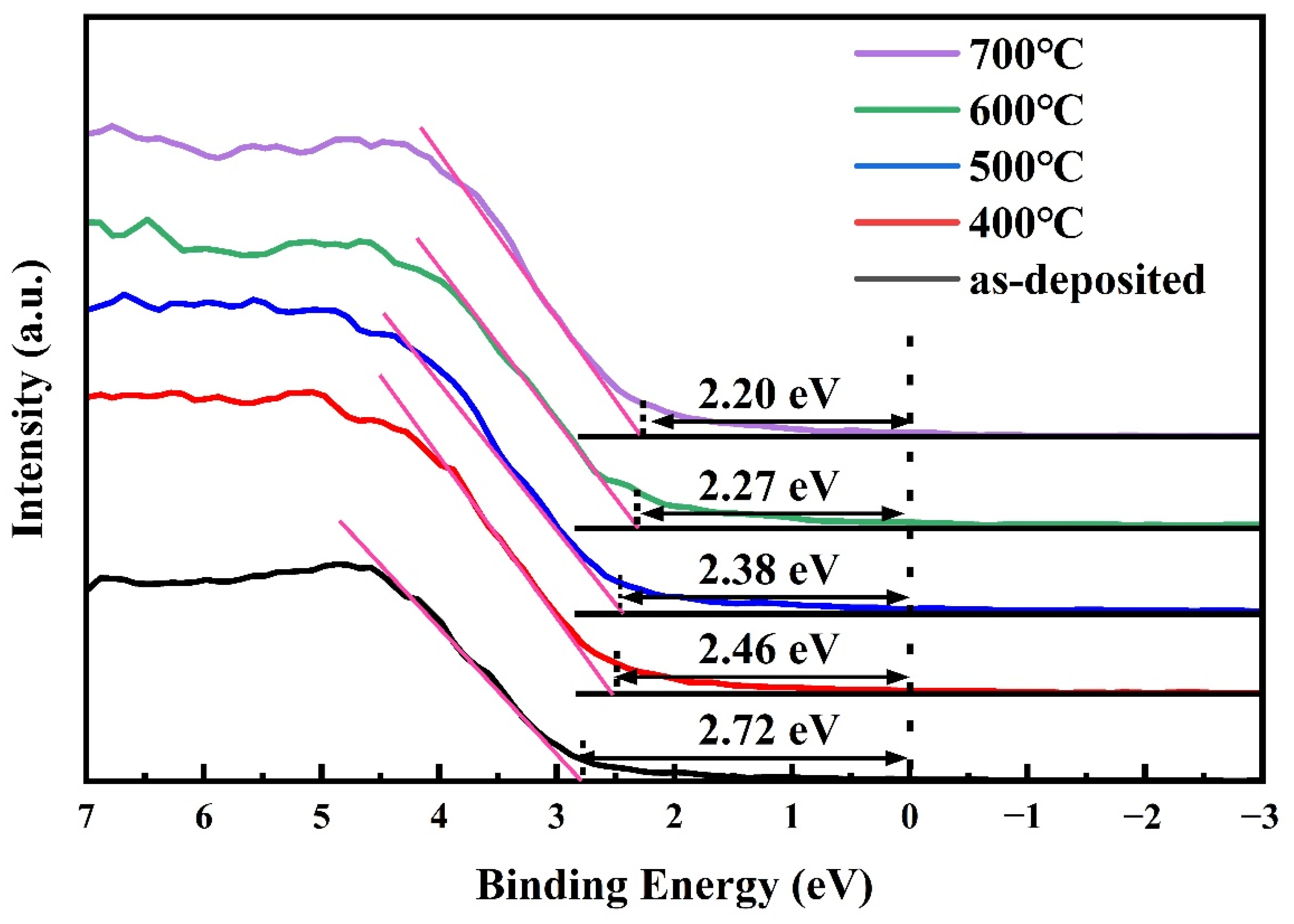
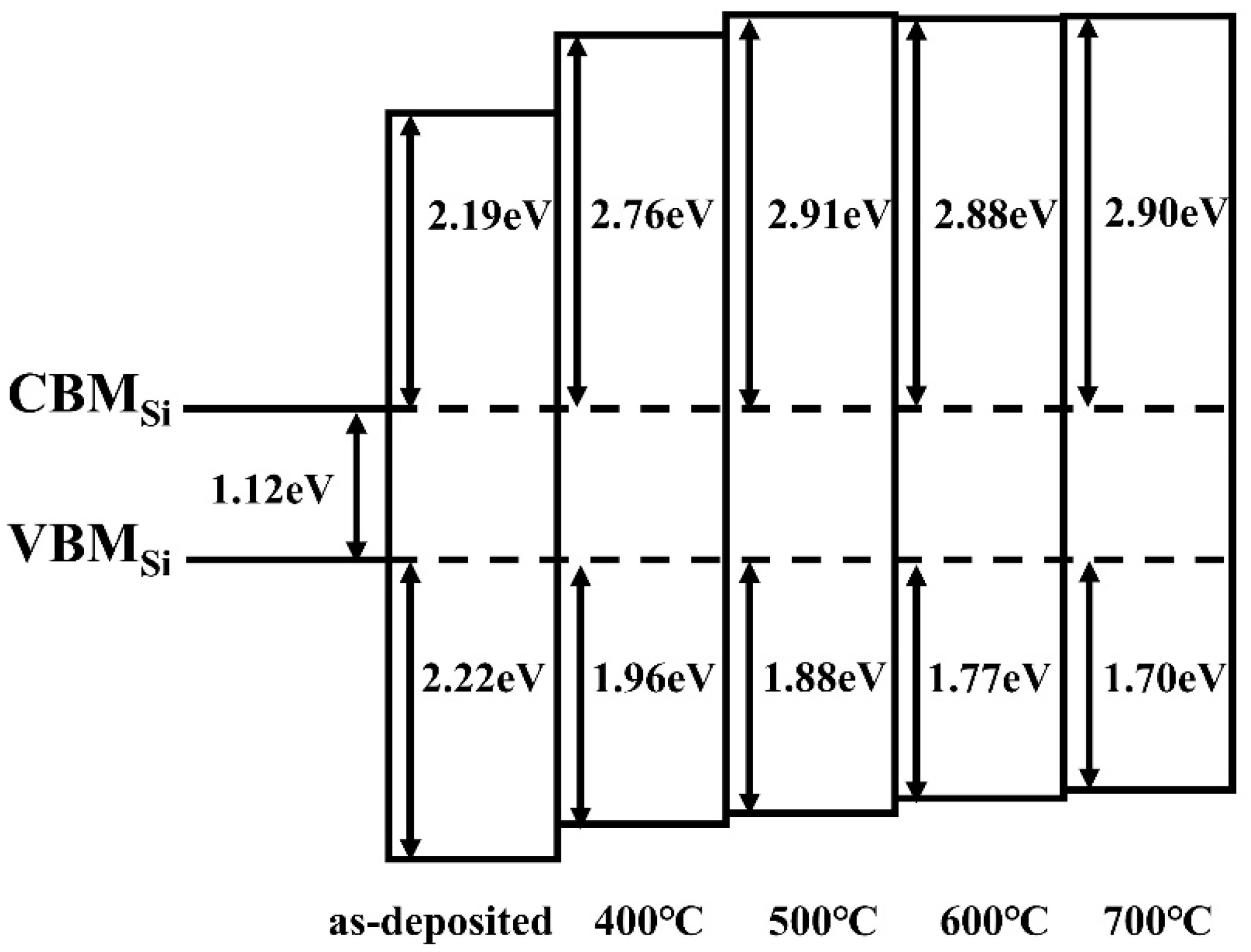
3.6. UV Spectral Analysis and Band Offset Determination

The transmission spectra of the quartz substrate in the HfO2 film doped with 5% La is shown in Figure 9. In the ultraviolet light region of 200–300 nm, the transmittance is significantly reduced due to the dispersion and absorption of the light in the ultraviolet band by the thin film sample. It can be seen from the figure that the transmittance of the unannealed thin film samples after wavelengths greater than 233 nm is higher than that of the other annealed samples. At the same time, with the increase in the annealing temperature, the transmittance in the ultraviolet region first increases and then decreases, and when the annealing temperature reaches the crystallization temperature, the transmittance increases again. This is attributed to the change in the absorption of the sample in this region due to the crystallization of the film. The average transmittance of all thin-film samples in the visible light region is greater than 80%, and the transmittance of the quartz sheet is 93%. Excluding the influence of the quartz substrate, the transmittance of all thin film samples in the visible light region is greater than 87%, which is due to the uniform composition of the components in the film. It shows that the film samples prepared by the sol–gel method have good forming effects.
The bandgap energy of semiconductors are important data for the study of thin-film transistors. The band gap of the film is obtained by the Tauc formula: (ahυ) = A(hυ − Eg)1/2 [43]. The absorption coefficient, Planck constant, frequency of light, and constant are represented in the equation by a, h, υ and A, respectively. By analyzing the Tauc chart in Figure 10, it is found that the band gap changes significantly before and after the sample is crystallized. The band gap of the as-deposited film is 5.53 eV. The band gaps after annealing are 5.84 and 5.91 eV at 400 and 500 °C, respectively. The band gap has increased significantly. This may be due to the fact that as the temperature increases, the atoms change from disorder to order. On the other hand, increasing the temperature can improve the overall quality of the film, reduce defects at the film interface and increase the band gap. Combined with the analysis results of the XPS spectrum, the reduction of oxygen vacancies can reduce the migration of electrons and increase the band gap. As the temperature increases from 600 to 700 °C, the band gap decreases to 5.77 and 5.72 eV. This might be due to sample crystallization, and the presence of silicate at the film’s interface layer will also cause the band gap to narrow.
The valence band offset (ΔEv) between the lanthanum-doped HfO2 film and the silicon substrate may be estimated using Kraut’s modeling approach by measuring the valence band maximum (VBM) between the film and the silicon substrate. The following formula is [40,41,42,43,44,45,46]:
ΔEv(LaHfO/Si) = Ev(LaHfO) − Ev(Si)
where VBM is determined by the edge of valence band through linear epitaxy. Figure 11 shows the valence band spectrum of the sample. The valence band values of the lanthanum-doped HfO2 film in the as-deposited state and under different annealing conditions at 400–700 °C are 2.72, 2.46, 2.38, 2.27 and 2.20 eV, respectively. As the temperature increases, the valence band value gradually decreases. According to the valence band of the silicon substrate is 0.5 eV, the valence band offset in the as-deposited state and at different annealing temperatures are 2.22, 1.96, 1.88, 1.77 and 1.70 eV, respectively.
Subtracting the valence band offset and the silicon substrate band gap from the band-gap energy of the lanthanum-doped HfO2 film yields the conduction band offset (ΔEc). The following is an equation [40,41,42,43,44,45,46]:
ΔEc(LaHfO/Si) = Eg(LaHfO) − ΔEv(LaHfO/Si) − Eg(Si)
where Eg(LaHfO) is the band gap of lanthanum-doped HfO2 films, obtained by depositing on a quartz substrate and by data obtained by UV-Vis transmission spectroscopy. We know that the band gap of the silicon substrate is 1.12 eV. Then the conduction band offset calculation results of the lanthanum-doped HfO2 film in the as-deposited state and under different annealing conditions at 400–700 °C are 2.19, 2.76, 2.91, 2.88, and 2.90 eV, respectively. Figure 12 shows the band diagram of the lanthanum-doped HfO2 film at different annealing temperatures on a silicon substrate. The results show that the conduction band offset and the valence band offset both exceed 1 eV, which can effectively limit the leakage current caused by the tunneling effect of electrons, and meet the minimum requirements of CMOS for the barrier height.

4. Conclusions

In summary, the optical properties, interface chemistry and energy band structure performance of the lanthanum-doped HfO2 thin film in the annealed state were systematically analyzed. It was found that the films prepared by sol–gel technology showed a short-range orderly monoclinic phase, and there was a tendency to preferentially grow with increasing temperature. The calculated grain sizes ranged from 17.1 to 22.4 nm on average. It was also confirmed from Raman spectroscopy that increasing the annealing temperature can improve the crystallinity of the films. In addition, the surface of the film is smooth, and the film has good interfacial contact with the silicon substrate. The presence of silicate in the interface layer improves the chemical state of the interface. Increasing the annealing temperature can effectively reduce the film thickness, making the film denser, and the thickness is reduced by 61.7%. Through XPS spectrum analysis, it is found that as the annealing temperature increases, the oxygen vacancies decrease significantly. The high optical transmittance of the lanthanum-doped HfO2 film in the visible light range is above 87%. At the same time, it exhibits a higher band gap width than a single HfO2. The band gap increases from 5.53 to 5.91 eV with the increasing annealing temperature. The calculated conduction band offset and valence band offset both exceed 1 eV. As a result, smaller grain size, good crystallinity and interfacial contact can be obtained by adjusting the annealing temperature. The higher conduction and valence band offsets meet the minimum barrier height requirements for CMOS.

Author Contributions

Data curation, formal analysis, writing—original draft, X.C.; conceptualization, project supervision, project administration, writing—review and editing, K.T.; formal analysis, methodology, H.C. and Z.L. All authors have read and agreed to the published version of the manuscript.

Funding

This research was supported by the National Natural Science Foundation of China (Grant No. 62141402), the Natural Science Foundation of Xinjiang Uygur Autonomous Region (Grand No. 2021D01C035), and was sponsored by Tianshan Innovation Team Program of Xinjiang Uygur Autonomous Region (Grand No. 2020D14038).

Institutional Review Board Statement

Not applicable.

Informed Consent Statement

Not applicable.

Data Availability Statement

Data are contained within the article.

Conflicts of Interest

The authors declare no conflict of interest.

References

  1. Cantas, A.; Aygun, G.; Turan, R. Impact of incorporated oxygen quantity on optical, structural and dielectric properties of reactive magnetron sputter grown high-κ HfO2/Hf/Si thin film. Appl. Surf. Sci. 2014, 318, 199–205. [Google Scholar] [CrossRef] [Green Version]
  2. Cheng, X.; Qi, Z.; Zhang, G.; Chen, Y.; Li, T.; Pan, G.; Yin, M. The interface reaction of high-k La2Hf2O7/Si thin film grown by pulsed laser deposition. Appl. Surf. Sci. 2009, 256, 838–841. [Google Scholar] [CrossRef]
  3. Xiong, K.; Robertson, J.; Gibson, M.C.; Clark, S.J. Defect energy levels in HfO2 high-dielectric-constant gate oxide. Appl. Phys. Lett. 2005, 87, 183505. [Google Scholar] [CrossRef] [Green Version]
  4. Wang, D.W.; Wang, Q.; Javey, A.; Tu, R.; Dai, H.J.; Kim, H.; McIntyre, P.C.; Krishnamohan, T.; Saraswat, K.C. Germanium nanowire field-effect transistors with SiO2 and high-κ HfO2 gate dielectrics. Appl. Phys. Lett. 2003, 83, 2432–2434. [Google Scholar] [CrossRef]
  5. Adelmann, C.; Sriramkumar, V.; Van Elshocht, S.; Lehnen, P.; Conard, T.; De Gendt, S. Dielectric properties of dysprosium- and scandium-doped hafnium dioxide thin films. Appl. Phys. Lett. 2007, 91, 162902. [Google Scholar] [CrossRef]
  6. Wilk, G.D.; Wallace, R.M.; Anthony, J.M. High-κ gate dielectrics: Current status and materials properties considerations. J. Appl. Phys. 2001, 89, 5243–5275. [Google Scholar] [CrossRef]
  7. He, G.; Deng, B.; Liu, M.; Ma, Y.; Chen, X.; Lv, J.; Sun, Z. Oxynitridization Dependent Interface Control and Band Alignment of AlON/SiON/Si Gate Stacks Grown by Metalorganic Chemical Vapor Deposition. Sci. Adv. Mater. 2013, 5, 709–712. [Google Scholar] [CrossRef]
  8. Sim, H.; Hwang, H.S. Effect of deuterium postmetal annealing on the reliability characteristics of an atomic-layer-deposited HfO2/SiO2 stack gate dielectrics. Appl. Phys. Lett. 2002, 81, 4038–4039. [Google Scholar] [CrossRef]
  9. Lee, H.; Jeon, S.; Hwang, H. Electrical characteristics of a Dy-doped HfO2 gate dielectric. Appl. Phys. Lett. 2001, 79, 2615–2617. [Google Scholar] [CrossRef]
  10. He, G.; Fang, Q.; Liu, M.; Zhu, L.; Zhang, L.Q.; Zhang, L.D. The structural and interfacial properties of HfO2/Si by the plasma oxidation of sputtered metallic Hf thin films. J. Cryst. Growth 2004, 268, 155–162. [Google Scholar] [CrossRef]
  11. Ahn, J.-H.; Kwon, S.-H. Sub-0.5 nm Equivalent Oxide Thickness Scaling for Si-Doped Zr1−xHfxO2 Thin Film without Using Noble Metal Electrode. ACS Appl. Mater. Interfaces 2015, 7, 15587–15592. [Google Scholar] [CrossRef] [PubMed]
  12. Chiang, C.-K.; Wu, C.-H.; Liu, C.-C.; Lin, J.-F.; Yang, C.-L.; Wu, J.-Y.; Wang, S.-J. Characterization of Hf1−xZrxO2 Gate Dielectrics with 0≤ x ≤ 1 Prepared by Atomic Layer Deposition for Metal Oxide Semiconductor Field Effect Transistor Applications. Jpn. J. Appl. Phys. 2011, 51, 11101. [Google Scholar] [CrossRef]
  13. Ye, C.; Zhan, C.; Zhang, J.Q.; Wang, H.; Deng, T.F.; Tang, S.R. Influence of rapid thermal annealing temperature on structure and electrical properties of high permittivity HfTiO thin film used in MOSFET. Microelectron. Reliab. 2014, 54, 388–392. [Google Scholar] [CrossRef]
  14. Liang, S.; He, G.; Zhu, L.; Zheng, C.Y.; Gao, J.; Wang, D.; Zhang, C.; Liu, M. Modulation of the microstructure, optical, and electrical properties of HfYO gate dielectrics by annealing temperature. J. Alloys Compd. 2018, 735, 1427–1434. [Google Scholar] [CrossRef]
  15. Ma, R.; Liu, M.; He, G.; Fang, M.; Shang, G.; Zhang, J.; Chen, X.; Gao, J.; Fei, G.; Zhang, L. Effects of rapid thermal annealing on interfacial and electrical properties of Gd-doped HfO2 high-k gate dielectrics. J. Alloys Compd. 2015, 646, 310–314. [Google Scholar] [CrossRef]
  16. Tang, L.; Chen, C.; Wei, A.; Li, K.; Zhang, D.; Zhou, K. Regulating crystal structure and ferroelectricity in Sr doped HfO2 thin films fabricated by metallo-organic decomposition. Ceram. Int. 2019, 45, 3140–3147. [Google Scholar] [CrossRef]
  17. Nohira, H.; Shiraishi, T.; Takahashi, K.; Hattori, T.; Kashiwagi, I.; Ohshima, C.; Ohmi, S.; Iwai, H.; Joumori, S.; Nakajima, K.; et al. Atomic-scale depth profiling of composition, chemical structure and electronic band structure of La2O3/Si(100) interfacial transition layer. Appl. Surf. Sci. 2004, 234, 493–496. [Google Scholar] [CrossRef]
  18. Mart, C.; Kühnel, K.; Kämpfe, T.; Zybell, S.; Weinreich, W. Ferroelectric and pyroelectric properties of polycrystalline La-doped HfO2 thin films. Appl. Phys. Lett. 2019, 114, 102903. [Google Scholar] [CrossRef]
  19. Schroeder, U.; Richter, C.; Park, M.H.; Schenk, T.; Pešić, M.; Hoffmann, M.; Fengler, F.P.G.; Pohl, D.; Rellinghaus, B.; Zhou, C.; et al. Lanthanum-Doped Hafnium Oxide: A Robust Ferroelectric Material. Inorg. Chem. 2018, 57, 2752–2765. [Google Scholar] [CrossRef]
  20. Pasko, S.; Abrutis, A.; Hubert-Pfalzgraf, L.G.; Kubilius, V. Cobalt (II) β-diketonate adducts as new precursors for the growth of cobalt oxide films by liquid injection MOCVD. J. Cryst. Growth 2004, 262, 653–657. [Google Scholar] [CrossRef]
  21. Chu, L.K.; Merckling, C.; Alian, A.; Dekoster, J.; Kwo, J.; Hong, M.; Caymax, M.; Heyns, M. Low interfacial trap density and sub-nm equivalent oxide thickness in In0.53Ga0.47As (001) metal-oxide-semiconductor devices using molecular beam deposited HfO2/Al2O3 as gate dielectrics. Appl. Phys. Lett. 2011, 99, 042908. [Google Scholar] [CrossRef]
  22. Aguilar-Castillo, A.; Aguilar-Hernández, J.R.; García-Hipólito, M.; López-Romero, S.; Swarnkar, R.; Báez-Rodríguez, A.; Fragoso-Soriano, R.J.; Falcony, C. White light generation from HfO2 films co-doped with Eu3++ Tb3+ ions synthesized by pulsed laser ablation technique. Ceram. Int. 2017, 43, 355–362. [Google Scholar] [CrossRef]
  23. Islamov, D.R.; Zalyalov, T.M.; Orlov, O.M.; Gritsenko, V.A.; Krasnikov, G.Y. Impact of oxygen vacancy on the ferroelectric properties of lanthanum-doped hafnium oxide. Appl. Phys. Lett. 2020, 117, 162901. [Google Scholar] [CrossRef]
  24. Suvorova, E.I.; Uvarov, O.V.; Arkharova, N.A.; Ibrayeva, A.D.; Skuratov, V.A.; Buffat, P.A. Structure evolution, bandgap, and dielectric function in La-doped hafnium oxide thin layer subjected to swift Xe ion irradiation. J. Appl. Phys. 2020, 128, 164103. [Google Scholar] [CrossRef]
  25. Gong, Y.-P.; Li, A.-D.; Qian, X.; Zhao, C.; Wu, D. Interfacial structure and electrical properties of ultrathin HfO2 dielectric films on Si substrates by surface sol-gel method. J. Phys. D Appl. Phys. 2008, 42, 015405. [Google Scholar] [CrossRef]
  26. Jin, P.; He, G.; Xiao, D.; Gao, J.; Liu, M.; Lv, J.; Liu, Y.; Zhang, M.; Wang, P.; Sun, Z. Microstructure, optical, electrical properties, and leakage current transport mechanism of sol-gel-processed high-k HfO2 gate dielectrics. Ceram. Int. 2016, 42, 6761–6769. [Google Scholar] [CrossRef]
  27. Kariper, I.A. Production of HfO2 thin films using different methods: Chemical bath deposition, SILAR and sol-gel process. Int. J. Miner. Met. Mater. 2014, 21, 832–838. [Google Scholar] [CrossRef]
  28. Kidchob, T.; Malfatti, L.; Serra, F.; Falcaro, P.; Enzo, S.; Innocenzi, P. Hafnia sol-gel films synthesized from HfCl4: Changes of structure and properties with the firing temperature. J. Sol-Gel Sci. Technol. 2007, 42, 89–93. [Google Scholar] [CrossRef]
  29. Leu, C.-C.; Chen, S.-T.; Liu, F.-K. Metal nanocrystal memory with sol–gel derived HfO2 high-κ tunnel oxide. Thin Solid Films 2011, 519, 5629–5633. [Google Scholar] [CrossRef]
  30. Tetzner, K.; Schroder, K.A.; Bock, K. Photonic curing of sol-gel derived HfO2 dielectrics for organic field-effect transistors. Ceram. Int. 2014, 40, 15753–15761. [Google Scholar] [CrossRef]
  31. Wang, Z.J.; Kumagai, T.; Kokawa, H.; Ichiki, M.; Maeda, R. Preparation of hafnium oxide thin films by sol-gel method. J. Electroceram. 2007, 21, 499–502. [Google Scholar] [CrossRef]
  32. Obstarczyk, A.; Kaczmarek, D.; Mazur, M.; Wojcieszak, D.; Domaradzki, J.; Kotwica, T.; Morgiel, J. The effect of post-process annealing on optical and electrical properties of mixed HfO2-TiO2 thin film coatings. J. Mater. Sci. Mater. Electron. 2019, 30, 6358–6369. [Google Scholar] [CrossRef] [Green Version]
  33. Battu, A.K.; Zade, V.B.; Deemer, E.; Ramana, C.V. Microstructure-Mechanical Property Correlation in Size Controlled Nanocrystalline Molybdenum Films. Adv. Eng. Mater. 2018, 20, 1800496. [Google Scholar] [CrossRef]
  34. Battu, A.K.; Makeswaran, N.; Ramana, C.V. Fabrication, characterization and optimization of high conductivity and high quality nanocrystalline molybdenum thin films. J. Mater. Sci. Technol. 2019, 35, 2734–2741. [Google Scholar] [CrossRef]
  35. Yan, K.; Yao, W.; Zhao, Y.; Yang, L.; Cao, J.; Zhu, Y. Oxygen vacancy induced structure change and interface reaction in HfO2 films on native SiO2/Si substrate. Appl. Surf. Sci. 2016, 390, 260–265. [Google Scholar] [CrossRef]
  36. Carlos, E.; Branquinho, R.; Kiazadeh, A.; Martins, J.; Barquinha, P.; Martins, R.; Fortunato, E. Boosting Electrical Performance of High-κ Nanomultilayer Dielectrics and Electronic Devices by Combining Solution Combustion Synthesis and UV Irradiation. ACS Appl. Mater. Interfaces 2017, 9, 40428–40437. [Google Scholar] [CrossRef] [PubMed]
  37. Lim, W.F.; Quah, H.J. Wet oxidation growth of hafnium doped tantalum oxide films with different composition deposited on silicon substrate. Appl. Surf. Sci. 2020, 526, 146722. [Google Scholar] [CrossRef]
  38. Zhao, X.; Vanderbilt, D. First-principles study of structural, vibrational, and lattice dielectric properties of hafnium oxide. Phys. Rev. B 2002, 65, 233106. [Google Scholar] [CrossRef] [Green Version]
  39. Tan, T.; Liu, Z.; Lu, H.; Liu, W.; Tian, H. Structure and optical properties of HfO2 thin films on silicon after rapid thermal annealing. Opt. Mater. 2010, 32, 432–435. [Google Scholar] [CrossRef]
  40. Zhang, Y.; He, G.; Wang, W.; Yang, B.; Zhang, C.; Xia, Y. Aqueous-solution-driven HfGdO gate dielectrics for low-voltage-operated α-InGaZnO transistors and inverter circuits. J. Mater. Sci. Technol. 2020, 50, 1–12. [Google Scholar] [CrossRef]
  41. Lin, S.-S.; Liao, C.-S. Effects of the ratio of O2/Ar pressure on wettability and optical properties of HfO2 films before and after doping with Al. Appl. Surf. Sci. 2016, 380, 229–236. [Google Scholar] [CrossRef]
  42. Chung, J.; Tak, Y.J.; Kim, W.-G.; Park, J.W.; Kim, T.S.; Lim, J.H.; Kim, H.J. Low-temperature fabrication of solution-processed hafnium oxide gate insulator films using a thermally purified solution process. J. Mater. Chem. C 2018, 6, 4928–4935. [Google Scholar] [CrossRef]
  43. Xiong, Y.; Tu, H.; Du, J.; Ji, M.; Zhang, X.; Wang, L. Band structure and electrical properties of Gd-doped HfO2 high k gate dielectric. Appl. Phys. Lett. 2010, 97, 012901. [Google Scholar] [CrossRef]
  44. Battu, A.K.; Manandhar, S.; Shutthanandan, V.; Ramana, C.V. Controlled optical properties via chemical composition tuning in molybdenum-incorporated beta-Ga2O3 nanocrystalline films. Chem. Phys. Lett. 2017, 684, 363–367. [Google Scholar] [CrossRef]
  45. Kumar, S.S.; Rubio, E.J.; Noor-A-Alam, M.; Martinez, G.; Manandhar, S.; Shutthanandan, V.; Thevuthasan, S.; Ramana, C.V. Structure, Morphology, and Optical Properties of Amorphous and Nanocrystalline Gallium Oxide Thin Films. J. Phys. Chem. C 2013, 117, 4194–4200. [Google Scholar] [CrossRef]
  46. Li, W.D.; He, G.; Zheng, C.Y.; Liang, S.; Zhu, L.; Jiang, S.S. Solution-processed HfGdO gate dielectric thin films for CMOS application: Effect of annealing temperature. J. Alloys Compd. 2018, 731, 150–155. [Google Scholar] [CrossRef]
Figure 1. XRD patterns of lanthanum-doped HfO2 films at different temperatures.
Coatings 12 00439 g001
Figure 2. (a) FTIR spectra of lanthanum-doped HfO2 films at different temperatures; (b) FTIR spectrum of 400–1400 cm−1 interval.
Coatings 12 00439 g002
Figure 3. Raman spectra of lanthanum-doped HfO2 films at different temperatures.
Coatings 12 00439 g003
Figure 4. (ae) SEM images of lanthanum-doped HfO2 thin films at different temperatures. (fj) SEM cross-sectional topography images at different temperatures.
Coatings 12 00439 g004
Figure 5. Broad-spectrum XPS spectra of lanthanum-doped HfO2 films at different temperatures.
Coatings 12 00439 g005
Figure 6. (ae) O 1s XPS spectra of lanthanum-doped HfO2 films at different temperatures. (f) O 1s XPS spectral stacking diagram.
Coatings 12 00439 g006
Figure 7. (ae) Hf 4f XPS spectra of lanthanum-doped HfO2 films at different temperatures. (f) Hf 4f XPS spectral stacking diagram.
Coatings 12 00439 g007
Figure 8. (ae) La 3d XPS spectra of lanthanum-doped HfO2 films at different temperatures. (f) La 3d XPS spectral stacking diagram.
Coatings 12 00439 g008
Figure 9. Transmission spectra of lanthanum-doped HfO2 films at different temperatures.
Coatings 12 00439 g009
Figure 10. (ae) Band gap values of lanthanum-doped HfO2 films at different temperatures.
Coatings 12 00439 g010
Figure 11. VB spectra of lanthanum-doped HfO2 films at different temperatures.
Coatings 12 00439 g011
Figure 12. Schematic bands of lanthanum-doped HfO2 thin films at different temperatures.
Coatings 12 00439 g012
Table 1. XPS analysis of the composition for lanthanum-doped HfO2 films as a function of annealing temperature.
SamplesComposition by XPS (at.%)
HfSiCOLa
As-deposited10.175.0250.433.720.68
400 ℃15.68.4133.7841.21
500 ℃16.138.2633.1241.441.05
600 ℃15.838.0735.2939.751.06
700 ℃16.18.0333.8840.831.16
Publisher’s Note: MDPI stays neutral with regard to jurisdictional claims in published maps and institutional affiliations.

