Article

Optoelectronic Properties of Hexagonal Boron Nitride Shielded Molybdenum Diselenide/Black-Phosphorus Based Heterojunction Field Effect Transistor

Department of Electrical Engineering, Chosun University, 375, Seosuk-dong, Dong-gu, Gwangju 501-759, Korea
*
Author to whom correspondence should be addressed.
Coatings 2022, 12(4), 445; https://doi.org/10.3390/coatings12040445
Submission received: 4 February 2022 / Revised: 19 March 2022 / Accepted: 22 March 2022 / Published: 25 March 2022

Abstract

:
Herein, we report the fabrication of a novel heterojunction field-effect transistor (HJFET) based on two-dimensional graphene (Gr), molybdenum diselenide (MoSe2), and black phosphorus (BP) that is shielded using hexagonal boron nitride to prevent device degradation. We perform electrical and optoelectronic characterizations of Gr/n-MoSe2 and Gr/n-MoSe2/p-BP heterojunctions. Heterojunction n-MoSe2/p-BP exhibits a potential barrier at the interface, which allows the use of BP as a top-gate contact to adjust the electrical and optoelectronic performances of the Gr/n-MoSe2 heterojunction. In the absence of a gate voltage, the Gr/n-MoSe2 and Gr/n-MoSe2/p-BP heterojunctions indicate photoresponsivity (Rλ) and specific detectivity (D*) of 1.77 AW−1 and 1.4 × 10¹⁰ cmHz1/2W−1, and 0.8 AW−1 and 0.3 × 10¹⁰ cmHz1/2W−1, respectively. The Gr/n-MoSe2 junction field-effect transistor with p-BP as gate contact demonstrates the best optoelectronic performance with high stability in terms of photoresponsivity Rλmax = 3.37 AW−1 and specific detectivity D*max = 3.16 × 10¹⁰ cmHz1/2W−1, rendering it extremely promising for photodetection applications.

1. Introduction

Layered two-dimensional (2D) materials offer the possibility of developing various electronic devices and sensors owing to the absence of dangling bonds [1]. In addition, the layers are associated with weak van der Waals interactions [2]; therefore, complex fabrication processes and lattice mismatches between thin films are no longer considered the main issues [3]. Graphene (Gr), which can be obtained by mechanically exfoliating graphite sheets, and Gr-like 2D materials, such as molybdenum diselenide (MoSe2), black phosphorus (BP), and hexagonal boron nitride (h-BN), have been widely investigated for their applications in electronic devices, sensors, and many other applications [4]. MoSe2 exhibits fascinating electronic and optoelectronic properties in its 2D form [5]. Meanwhile, h-BN is a dielectric material with a large bandgap of ~6 eV, rendering it useful as an oxide layer for MOS devices [6] and as a dielectric for device shielding [7]. In addition, BP is a promising 2D material due to its infrared bandgap energy, which can be adjusted from ~0.3 eV (bulk) to ~2 eV (monolayer) by reducing the layer thickness [8,9]. BP-based heterojunctions have been investigated for photocatalytic water splitting [10], tunable multivalued logic devices [11], mid-infrared light-emission applications [9], carbon dioxide (CO2) reduction [12], and broadband photodetectors [13]. A black-phosphorus/molybdenum diselenide heterojunction (n-MoSe2/p-BP) was prepared and investigated for low-power photodetection applications for the first time by our group, where the device demonstrated a photoresponsivity, an external quantum efficiency, a normalized photocurrent-to-dark-current ratio, and a specific detectivity of 3.2 mAW−1, 31.4 × 10¹² W−1, 0.74%, and 1.4 × cmHz1/2W−1, respectively, at an extremely low polarization voltage [14].
In this study, we improved the structure of our previous photodetector based on n-MoSe2/p-BP [14], where the observed photoresponsivity values can be explained based on the Schottky barrier between MoSe2 and metallic electrodes. In this study, we added multilayered Gr between MoSe2 and a metallic electrode and successfully improved the performance of a Gr/MoSe2-based photodetector. Moreover, we investigated the effect of Gr and BP contacts on the electrical and optoelectronic performances of the device. Finally, we discuss the possibility of using BP as a top gate to create a tunable photodetector.

2. Materials and Methods

MoSe2, BP, h-BN, and Gr were purchased from HQ Graphene. First, four chromium/gold (10/50 nm) electrodes were deposited via thermal evaporation onto an oxidized p-type silicon (Si) substrate comprising a 300 nm-thick silicon oxide (SiO2) layer. Thereafter, multilayered Gr, MoSe2, and BP were deposited onto the metallic electrodes via mechanical exfoliation [15]. Finally, multilayered h-BN was deposited on top of the as-fabricated device using the same deposition technique. Figure S1a shows an optical image of the fabricated Gr/n-MoSe2/p-BP heterostructures. The device was shielded with 2D h-BN to prevent device oxidation and protect the BP from degradation, as shown in Figure S1b. Figure S1c shows a schematic illustration of the device before and after shielding. The current device was annealed at 200 °C for 5 min under nitrogen gas to improve the contact quality, unlike the procedure reported in [14]. We used a Hitachi S-4800 instrument to perform scanning electron microscopy (SEM) imaging and a Park NX20 atomic force microscope to acquire atomic force microscopy (AFM) images. Electrical and optoelectronic characterizations were performed using an HP 4155A semiconductor parameter analyzer, where laser power values ranging from 0.016 to 12.37 μW were set, and the wavelength and spot diameter were 532 nm and 20 μm, respectively.

3. Results and Discussion

3.1. Morphological Characterization

Figure 1a shows the SEM images of h-shielded Gr/n-MoSe2/p-BP heterostructures, where Gr, MoSe2, BP, and h-BN flakes are outlined by dashed blue, green, orange, and red lines, respectively. As shown in the same figure, the device length was 20 µm. Figure 1b shows the AFM image, where the blue, green, and red lines in Figure 1c indicate the respective cross-sections of the Gr, MoSe2, BP, and h-BN flakes, respectively. Based on the topographic analysis, the thicknesses of the Gr, MoSe2, BP, and h-BN flakes were 40, 60, 80, and 110 nm, as shown in the same figure. The surface areas of the pn (n-MoSe2/p-BP) junction and n-MoSe2 flake were estimated to be 2.02 × 10⁻⁶ and 3.2 × 10⁻⁶ cm2, respectively.

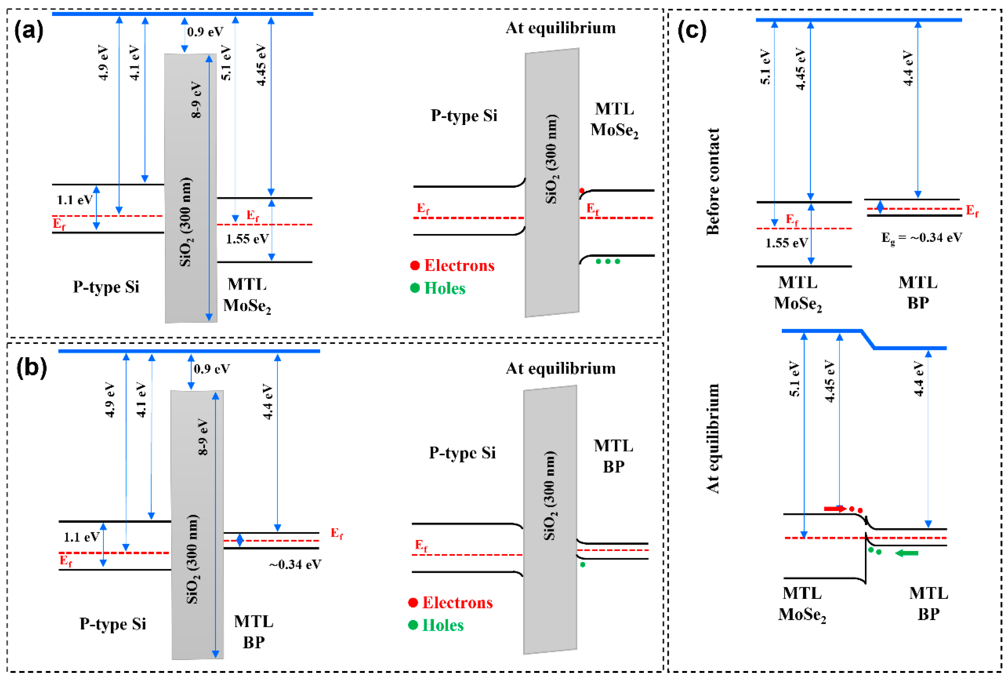
3.2. Energy Band Diagrams

Figure 2 shows the energy band diagrams of multilayered BP and MoSe2 before and after contact on Si/SiO2 substrate in the vertical direction. As shown, holes and electrons accumulated at the SiO2/p-BP and SiO2/n-MoSe2 interfaces, respectively, which implies that both the Gr/n-MoSe2/Au-and Au/p-BP/Au-based field-effect transistor devices are typically switched on. As shown in Figure 2c, the multilayered n-MoSe2 and p-BP exhibited straddling alignment (type I), with a small electron barrier in the conduction band and a large hole barrier in the valence band. The multilayered n-MoSe2 formed a double Schottky contact with the gold contacts [14]; therefore, we added multilayered Gr on one side to reduce the Schottky barrier between gold and multilayered n-MoSe2 because the work function of Gr is in a similar range to that of graphite, i.e., ~4.6 eV [16].

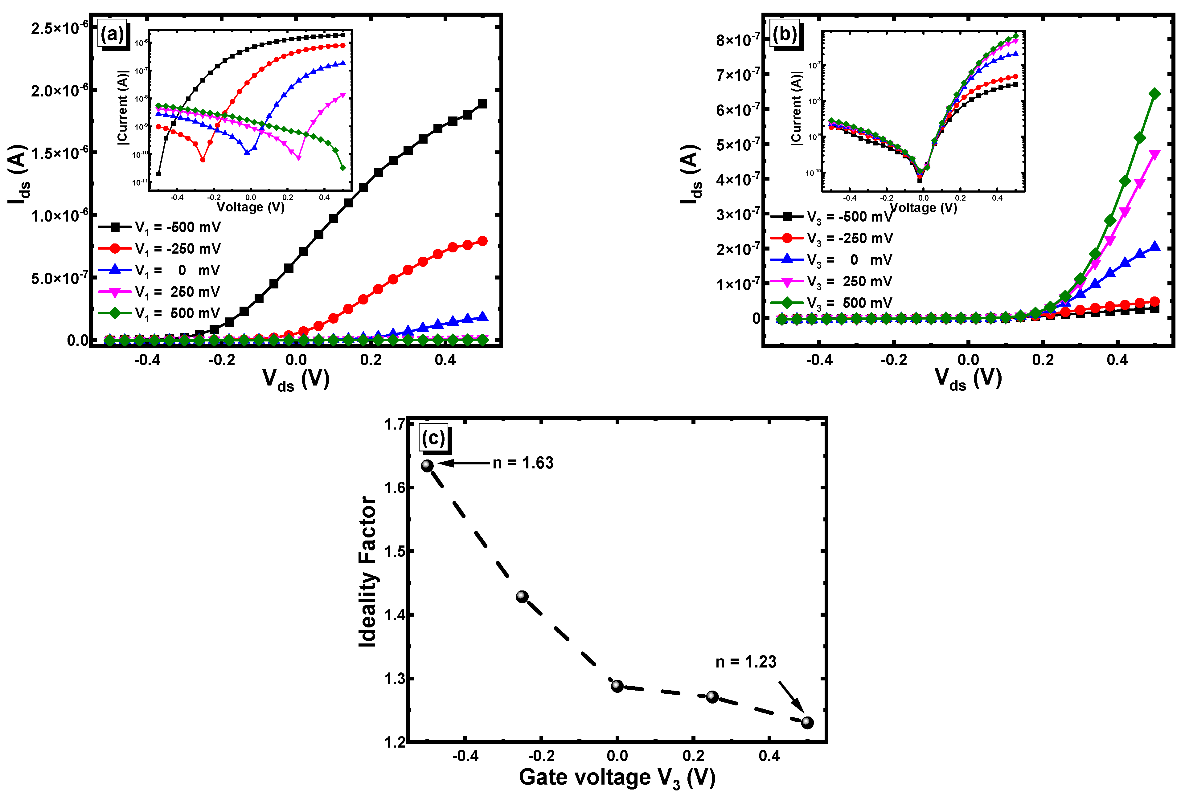
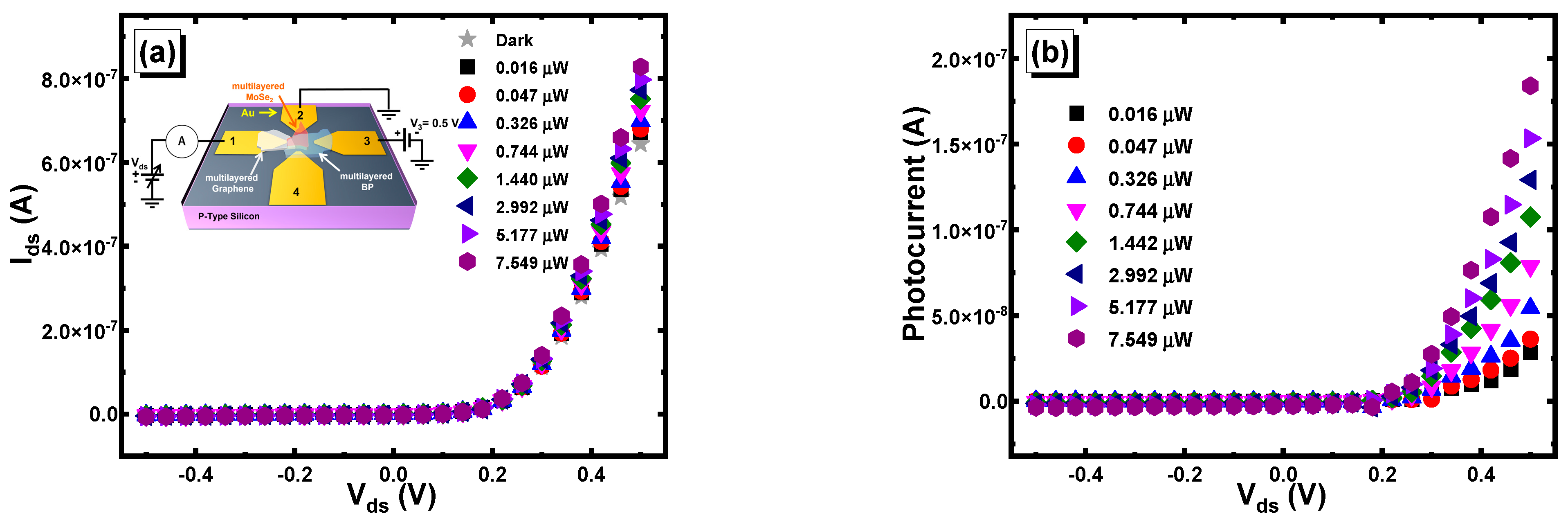
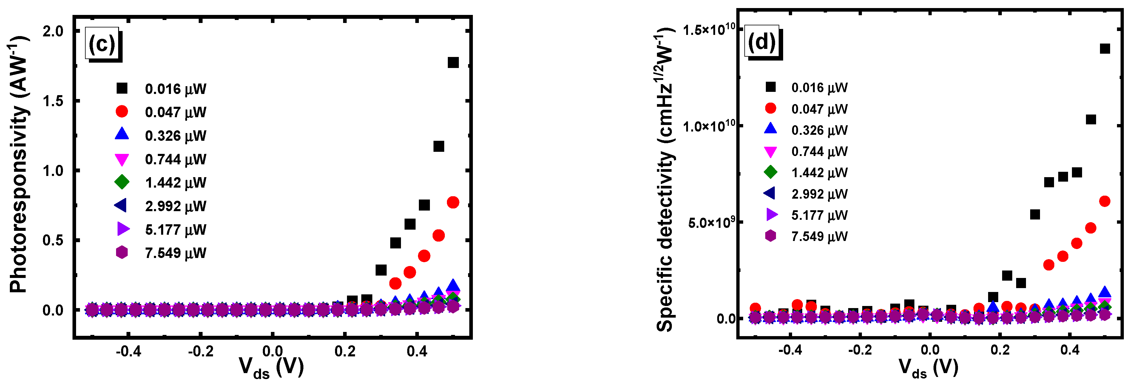
3.3. Electrical and Optoelectronic Characterization

As shown in Figure S2a–d, the shielding slightly affected the electrical characteristics, which is likely due to the mechanical pressure that emerged during the deposition of the h-BN flakes. In addition, annealing significantly improved the electrical performance of the device. Moreover, as shown in Figure S2b, Gr/n-MoSe2 exhibited better electrical performance than the device reported in our previous paper [14].
We performed optoelectronic measurements in the absence of a polarization voltage, i.e., in the absence of a gate polarization voltage. Figure 3a shows the output characteristics of the Gr/n-MoSe2/p-BP heterojunction in the dark and at different values of laser power, and the corresponding photoresponsivity Rλ (Figure 3b) was calculated using the equation Rλ = |Iph|/P = |IlightIdark|/P, where Iph represents the photocurrent and P the laser power. The output characteristics and photoresponsivity of the Gr/n-MoSe2 heterostructures are shown in Figure 3c and d, respectively. As presented, G/n-MoSe2 showed more stability in terms of photoresponsivity compared with the Gr/n-MoSe2/p-BP heterojunction, where the photoresponsivity varied homogeneously as a function of the polarization voltage, with a maximum value of 1.96 AW−1 recorded at a polarization voltage of 0.5 V.
Figure 4a shows the output characteristics in the dark condition of n-MoSe2/p-BP when MTL Gr was used as the gate. The current (Ids or I32) and voltage (Vds or V32) were measured between contacts (2) and (3), and the gate voltage (V1) was applied at contact (1) (see Figure S3a). As shown in Figure 4a, the n-MoSe2/p-BP heterojunction indicated a p-type channel, which implies that the transport was dominated by holes in the valence band in BP (Figure 2b,c). The shift in the drain–source voltage to negative values as the gate voltage increased, as observed in the n-MoSe2/p-BP heterojunction and illustrated in the inset of Figure 2a, was due to the leakage current between the multilayered Gr and MoSe2 flakes. Figure 4b shows the output characteristics in the dark condition of Gr/n-MoSe2 when MTL BP was used as the gate. The current (Ids or I12) and voltage (Vds or V12) were measured between contacts (1) and (2), and the gate voltage (V3) was applied at contact (3) (see Figure S4a). The Gr/MoSe2 heterojunction indicated an n-type channel; therefore, the transport was dominated by electrons accumulated at the SiO2/n-MoSe2 interface and in the multilayered n-MoSe2 (Figure 2a). As illustrated in the inset of Figure 4b, the device indicated an extremely low leakage current and a high on/off current (Ion/Ioff = 6.3 × 10³ at a gate voltage of 0.5 V), which can be explained by the potential barrier between n-MoSe2 and p-BP (see Figure 2c). It is noteworthy that both Gr/n-MoSe2 and n-MoSe2/p-BP were in the accumulated mode, as shown in Figure 2a,b.
Because Gr/n-MoSe2 exhibited good output characteristics, we investigated the variation in its ideality factor as a function of the applied gate voltage. The ideality factor (n) can be deduced from the relationship between current and voltage in a diode, expressed as Id = IS(exp(qVd/nkBT) − 1), where IS is the reverse saturation current, q the elementary electron charge, kB the Boltzmann constant, T the temperature, and Vd is the applied voltage. As shown in Figure 4c, the ideality factor of the Au/Gr/n-MoSe2/Au heterojunction can be adjusted from 1.63 to 1.23 by changing the gate voltage applied in the multilayered BP contact from −0.5 to 0.5 V.
We investigated the electrical and optoelectronic characteristics comprehensively. Figure S3 shows a schematic illustration of the electrical polarization configuration of n-MoSe2/p-BP when MTL Gr was used as the gate and the corresponding output characteristics at different values of laser power. Figure 5a shows the output characteristics for the same configuration (Figure S3a) at a constant gate voltage (VG = V1 = −0.5 V). Figure 5b–d show the photocurrent, photoresponsivity, and specific detectivity deduced for the same polarization configuration, respectively. The specific detectivity (D*) was determined using the following equation:
D * = R λ × ( A ) 0.5 / ( 2 e I d a r k ) 0.5 ,
where e is the charge of an elementary electron, and A is the effective area of the photodetector approximated as the surface areas of the n-MoSe2/p-BP junction (2.02 × 10⁻⁶ cm2) and n-MoSe2 flake (3.2 × 10⁻⁶ cm2). The n-MoSe2/p-BP heterojunction indicated an increase in the photocurrent, photoresponsivity, and specific detectivity as the polarization voltage (Vds or V32) and laser power increased; however, the values of photoresponsivity and specific detectivity varied inhomogeneously when the polarization voltage increased, which was likely due to the leakage current from the gate contact (MTL Gr).
Figure 6a shows the output characteristics for the same configuration (as shown in Figure S4a) at a constant gate voltage (VG = V3 = 0.5 V) applied at the MTL p-BP. We fixed the gate voltage at 0.5 V since this value yielded the highest values of current Ids (or I12), as shown in Figure S4.
Figure 5b,c, and d show the photocurrent, photoresponsivity, and specific detectivity of the Gr/n-MoSe2 heterojunction, respectively. The photoresponsivity and specific detectivity increased homogenously as the polarization voltage (Vds or V32) increased, and the maximum values recorded were 1.77 AW−1 and 1.4 × 10¹⁰ cmHz1/2W−1, respectively, at a gate voltage of 0.5 V.
Subsequently, we characterized the Ids–VG (or I12–V3) of Gr/n-MoSe2 when MTL p-BP was used as the gate electrode, as shown in Figure S5 and Figure 7a. Figure S5b–j show the transfer characteristics at different values of laser power and drain–source voltage (Vds or V12), which varied between 0.1 and 0.5 V. Figure 7 shows the electrical and optoelectronic properties at a drain–source voltage of 0.5 V. As shown in Figure 7c,d, this configuration yielded the best optoelectronic performance, where the photoresponsivity and specific detectivity exhibited the best homogenous variation at a positive drain–source voltage, where maximum values of 3.37 AW−1 and 3.16 × 10¹⁰ cmHz1/2W−1, respectively, were recorded at a gate voltage of 0.5 V.
In summary, we successfully created a new junction field-effect transistor. We investigated all the possible configurations to determine the ideal configuration that yields the best optoelectronic performance. The Gr/n-MoSe2 heterojunction with an MTL p-BP as the gate voltage demonstrated the best optoelectronic performance, affording maximum photoresponsivity and specific detectivity values of 3.37 AW−1 and 3.16 × 10¹⁰ cmHz1/2W−1, respectively, which are higher than those of BP-based photodetector reported previously [14,17,18]. However, those values were lower than those reported by Guo et al. [19], where a maximum photoresponsivity of 82 AW−1 was recorded at the same polarization voltage as that used in our study (0.5 V) and at approximately the same range of laser power value. However, it is noteworthy that in their study, multiple interdigitated electrodes were used to optimize the photocarrier collection efficiency, with a spacing of 1 µm between the electrodes, which improved the optoelectronic performance.

4. Conclusions

In conclusion, we fabricated Gr/n-MoSe2/p-BP heterojunctions using 2D materials. We investigated their electrical and optoelectronic properties based on different configurations. Gr/n-MoSe2 and Gr/n-MoSe2/p-BP heterojunctions exhibited promising optoelectronic properties, and both can be used for photodetection applications. Meanwhile, BP was used as the gate contact owing to its potential barrier formed at the interface with n-MoSe2, which allows the tuning of its electrical and optoelectronic performances, such as the ideality factor, photoresponsivity, and specific detectivity, to values of 1.23, 3.37 AW−1, and 3.16 × 10¹⁰ cmHz1/2W−1, respectively. In future research, the high-κ dielectric can be used as a gate insulator with the aim of solving the leakage current between the gate contact and the active channel. Moreover, we believe that the performance of our new photodetector can be improved using multiple interdigitated electrodes and by reducing the channel length.

Supplementary Materials

The following supporting information can be downloaded at: https://www.mdpi.com/article/10.3390/coatings12040445/s1, Figure S1: Optical images of (a) Gr/n-MoSe2/p-BP and (b) Gr/n-MoSe2/p-BP shielded by h-BN, and (c) schematic of the device before and after shielding; Figure S2: Electrical properties of the as-fabricated device, h-BN-covered device and h-BN-covered device after annealing of (a) Black-phosphorous (BP) (I34–V34), (b) graphene/n-MoSe2 (I12–V12), (c) n-MoSe2/p-BP (I23–V23), and (d) Gr/n-MoSe2/p-BP (I13–V13); Figure S3: (a) Schematic illustration of electrical polarization configuration of n-MoSe2/p-BP when MTL Gr is used as gate, and its output characteristics at (b) dark, (c) 0.016 µW, (d) 0.047 µW, (e) 0.326 µW, (f) 0.744 µW, (g) 1.442 µW, (h) 2.992 µW, (i) 5.177 µW, and (j) 7.549 µW; Figure S4: (a) Schematic illustration of electrical polarization configuration of Gr/n-MoSe2 when MTL p-BP is used as gate, and its output characteristics at (b) dark, (c) 0.016 µW, (d) 0.047 µW, (e) 0.326 µW, (f) 0.744 µW, (g) 1.442 µW, (h) 2.992 µW, (i) 5.177 µW, and (j) 7.549 µW; Figure S5: (a) Schematic illustration of electrical polarization configuration of Gr/n-MoSe2 when MTL p-BP is used as gate, and its IDS–VG Transfer characteristics at (b) dark, (c) 0.016 µW, (d) 0.047 µW, (e) 0.326 µW, (f) 0.744 µW, (g) 1.442 µW, (h) 2.992 µW, (i) 5.177 µW, and (j) 7.549 µW.

Author Contributions

Methodology, C.W.; writing—original draft preparation, A.A.; writing—review and editing, P.-J.K. All authors have read and agreed to the published version of the manuscript.

Funding

This work was supported by the Brain Pool Program through the National Research Foundation of Korea (NRF) funded by the Ministry of Science and ICT (NRF-2019H1D3A1A01102658), and this study was supported by a research fund from Chosun University, 2021.

Institutional Review Board Statement

Not applicable.

Informed Consent Statement

Not applicable.

Data Availability Statement

Data are available from the corresponding author upon the request.

Conflicts of Interest

The authors declare no conflict of interest.

References

  1. Paletti, P.; Yue, R.; Hinkle, C.; Fullerton-Shirey, S.K.; Seabaugh, A. Two-dimensional electric-double-layer Esaki diode. NPJ 2D Mater. Appl. 2019, 3, 1–7. [Google Scholar] [CrossRef]
  2. Liu, Y.; Huang, Y.; Duan, X. Van der Waals integration before and beyond two-dimensional materials. Nature 2019, 567, 323–333. [Google Scholar] [CrossRef] [PubMed]
  3. Fang, Y.; Ge, Y.; Wang, C.; Zhang, H. Mid-infrared photonics using 2D materials: Status and challenges. Laser Photonics Rev. 2020, 14, 1900098. [Google Scholar] [CrossRef]
  4. Xu, M.; Liang, T.; Shi, M.; Chen, H. Graphene-like two-dimensional materials. Chem. Rev. 2013, 113, 3766–3798. [Google Scholar] [CrossRef] [PubMed]
  5. Abderrahmane, A.; Oh, J.M.; Kim, N.H.; Ko, P.J.; Sandhu, A. Micro-Hall sensors based on two-dimensional molybdenum diselenide. J. Nanosci. Nanotechnol. 2019, 19, 4330–4332. [Google Scholar] [CrossRef] [PubMed]
  6. Abderrahmane, A.; Ko, P.J.; Jung, P.G.; Kim, N.H.; Sandhu, A. Optoelectronic characterizations of two-dimensional h-BN/MoSe2 heterostructures based photodetector. Sci. Adv. Mater. 2018, 10, 627–631. [Google Scholar] [CrossRef]
  7. Li, A.; Chen, Q.; Wang, P.; Gan, Y.; Qi, T.; Wang, P.; Tang, F.; Wu, J.Z.; Chen, R.; Zhang, L.; et al. Ultrahigh-sensitive broadband photodetectors based on dielectric shielded MoTe2/Graphene/SnS2 p–g–n junctions. Adv. Mater. 2019, 31, 1805656. [Google Scholar] [CrossRef] [PubMed]
  8. Li, J.; Luo, H.; Zhai, B.; Lu, R.; Guo, Z.; Zhang, H.; Liu, Y. Black phosphorus: A two-dimension saturable absorption material for mid-infrared Q-switched and mode-locked fiber lasers. Sci. Rep. 2016, 6, 30361. [Google Scholar] [CrossRef] [PubMed] [Green Version]
  9. Zong, X.; Hu, H.; Ouyang, G.; Wang, J.; Shi, R.; Zhang, L.; Zeng, Q.; Zhu, C.; Chen, S.; Cheng, C.; et al. Black phosphorus-based van der Waals heterostructures for mid-infrared light-emission applications. Light Sci. Appl. 2020, 9, 1–8. [Google Scholar] [CrossRef]
  10. Liu, F.; Huang, C.; Liu, C.X.; Shi, R.; Chen, Y. Black Phosphorus-Based Semiconductor Heterojunctions for Photocatalytic Water Splitting. Chem. Eur. J. 2020, 26, 4449–4460. [Google Scholar] [CrossRef]
  11. Hassan, Y.; Srivastava, P.K.; Singh, B.; Abbas, M.S.; Ali, F.; Yoo, W.J.; Lee, C. Phase-engineered molybdenum telluride/black phosphorus van der waals heterojunctions for tunable multivalued logic. ACS Appl. Mater. Interfaces 2020, 12, 14119–14124. [Google Scholar] [CrossRef] [PubMed]
  12. Chen, C.; Hu, J.; Yang, X.; Yang, T.; Qu, J.; Guo, C.; Li, C.M. Ambient-stable black phosphorus-based 2D/2D S-scheme heterojunction for efficient photocatalytic CO2 reduction to syngas. ACS Appl. Mater. Interfaces 2021, 13, 20162–20173. [Google Scholar] [CrossRef] [PubMed]
  13. Krishnamurthi, V.; Low, M.X.; Kuriakose, S.; Sriram, S.; Bhaskaran, M.; Walia, S. Black phosphorus nanoflakes vertically stacked on MoS2 nanoflakes as heterostructures for photodetection. ACS Appl. Nano Mater. 2021, 4, 6928–6935. [Google Scholar] [CrossRef]
  14. Abderrahmane, A.; Woo, C.; Ko, P.J. Black phosphorus/molybdenum diselenide heterojunction-based photodetector. J. Electron. Mater. 2021, 50, 5713–5720. [Google Scholar] [CrossRef]
  15. Gao, E.; Lin, S.Z.; Qin, Z.; Buehler, M.J.; Feng, X.Q.; Xu, Z. Mechanical exfoliation of two-dimensional materials. J. Mech. Phys. Solids 2018, 115, 248–262. [Google Scholar] [CrossRef]
  16. Yu, Y.J.; Zhao, Y.; Ryu, S.; Brus, L.E.; Kim, K.S.; Kim, P. Tuning the graphene work function by electric field effect. Nano Lett. 2009, 9, 3430–3434. [Google Scholar] [CrossRef] [PubMed] [Green Version]
  17. Hou, C.; Yang, L.; Li, B.; Zhang, Q.; Li, Y.; Yue, Q.; Wang, Y.; Yang, Z.; Dong, L. Multilayer black phosphorus near-infrared photodetectors. Sensors 2018, 18, 1668. [Google Scholar] [CrossRef] [PubMed] [Green Version]
  18. Hong, T.; Chamlagain, B.; Wang, T.; Chuang, H.J.; Zhou, Z.; Xu, Y.Q. Anisotropic photocurrent response at black phosphorus–MoS2 p–n heterojunctions. Nanoscale 2015, 7, 18537–18541. [Google Scholar] [CrossRef] [PubMed]
  19. Guo, Q.; Pospischil, A.; Bhuiyan, M.; Jiang, H.; Tian, H.; Farmer, D.; Deng, B.; Li, C.; Han, S.J.; Wang, H.; et al. Black phosphorus mid-infrared photodetectors with high gain. Nano Lett. 2016, 16, 4648–4655. [Google Scholar] [CrossRef] [PubMed] [Green Version]
Figure 1. (a) Scanning electron microscopy (SEM) image (scale: 20 µm), (b) atomic force microscopy (AFM) image (scale: 20 µm) of h-BN-covered Gr/n-MoSe2/p-BP heterostructures, and (c) the corresponding thickness of each multilayer determined via topographic analysis.
Coatings 12 00445 g001
Figure 2. Energy band diagram of multilayered (a) n-MoSe2 and (b) p-BP before and after contact in the vertical direction and that of (c) n-MoSe2/p-BP before and after contact.
Coatings 12 00445 g002
Figure 3. Laser power dependence of output characteristics of (a) Gr/n-MoSe2/p-BP and (c) Gr/n-MoSe2 heterojunctions, and (b,d) their corresponding absolute values of photoresponsivity.
Coatings 12 00445 g003
Figure 4. Output characteristics in dark conditions of (a) n-MoSe2/p-BP when MTL Gr was used as the gate and (b) Gr/n-MoSe2 when MTL p-BP was used as the gate; (c) ideality factor of Au/Gr/n-MoSe2/Au heterojunction vs. gate voltage.
Coatings 12 00445 g004
Figure 5. Polarization voltage and laser power dependence in n-MoSe2/p-BP heterojunction: (a) Output characteristics (Ids–Vds or I32–V32), (b) photocurrent, (c) photoresponsivity, and (d) specific detectivity at gate voltage (VG or V1) of −0.5 V.
Coatings 12 00445 g005
Figure 6. Polarization voltage and laser power dependence in Gr/n-MoSe2 heterojunction: (a) Output characteristics (Ids–Vds or I12–V12), (b) photocurrent, (c) photoresponsivity, and (d) specific detectivity at gate voltage (VG or V3) of 0.5 V.
Coatings 12 00445 g006aCoatings 12 00445 g006b
Figure 7. Gate voltage and laser power dependence in Gr/n-MoSe2 heterojunction: (a) Transfer characteristic Ids–VG (or I12–V3), (b) photocurrent, (c) photoresponsivity, and (d) specific detectivity at drain–source voltage (Vds or V12) of 0.5 V.
Coatings 12 00445 g007
Publisher’s Note: MDPI stays neutral with regard to jurisdictional claims in published maps and institutional affiliations.

