Abstract
The homoepitaxial Si-doped Ga2O3 film prepared by metal–organic chemical vapor deposition (MOCVD) was reported in this paper. The film thickness reached 4.5 microns, a relatively high value for MOCVD. The full width at half maxima of the (002) diffraction plane of the film was 26.3 arcsec, thus showing high crystalline quality. The film showed n−-type properties with a doping concentration of 3.6 × 1016 cm−3 and electron mobility of 137 cm2/V·s. In addition, the element composition and stress state of the film were characterized and analyzed. This indicates that the MOCVD, supporting high-quality, high-precision epitaxy, is promising for Ga2O3 power devices.
1. Introduction
Ga2O3 is an ultra-wide bandgap semiconductor material with a bandgap of 4.9 eV, high ultraviolet–visible light transmittance and a theoretical breakdown electric field strength as high as 8 mV/cm, which gives it broad applications in optoelectronic devices and power devices [1,2,3,4,5]. Furthermore, large-sized Ga2O3 single crystals can be directly obtained by melt growth, which facilitates the homoepitaxy of high-quality Ga2O3 films, thereby greatly improving the device’s performance [6,7,8]. Common vapor deposition, such as halide vapor phase epitaxy (HVPE) [9], magnetron sputtering [10], MOCVD [11,12], mist-CVD [13], molecular beam epitaxy (MBE) [14], etc., can be adopted for the growth of Ga2O3 films, also accelerating the application of Ga2O3 devices. Currently, Ga2O3 power rectifiers are mainly based on Schottky barrier diodes (SBDs) and heterojunction diodes (HJDs) [5,15,16,17,18,19]. The fabrication of Ga2O3 SBDs and HJDs is based on drift layers with low doping concentration and high thickness since a higher drift-layer thickness is beneficial to significantly improve the breakdown voltage of the devices and thus improve the power figure of merit. In the preparation technology of Ga2O3 films, it is challenging to meet the above-two requirements simultaneously. At present, only a few institutions have achieved the production of high-thickness Ga2O3 epitaxial wafers through HVPE due to its fast growth speed [20]. Compared with HVPE, MOCVD has advantages in growth cost, accuracy, and repeatability, which have been demonstrated in previous research [21]. More importantly, Farzana et al. have proved the advantages of diodes made of Ga2O3 films grown by MOCVD in structural design flexibility and with resistance [22]. However, the preparation of Ga2O3 films with thickness up to several micrometers by MOCVD has not been reported.
In this study, to demonstrate the possibility of preparing high-thickness Ga2O3 films by MOCVD, the n-type β-Ga2O3 films with high thickness for SBDs and HJDs were grown by MOCVD, and the properties of the films were characterized.
2. Materials and Methods
2.1. Materials
The growth was performed on the double-sided polished (001) β-Ga2O3 substrates, purchased from Novel Crystal Technology, Inc. (Saitama, Japan). High-purity O2 (5N) and trimethylgallium (TMGa, 6N) were used as the oxygen and gallium source for the MOCVD apparatus (Emcore D180), respectively. The doping source for the n-type β-Ga2O3 films is a mixed gas of SiH4 and N2 (SiH4, 100 ppm). High-purity N2 (5N) and Ar (5N) were used as carrier gas for oxygen source and TMGa, respectively.
2.2. Experiment
The substrates were ultrasonically cleaned for 5 min with acetone, ethanol, and deionized water, then dried with N2 before being put in the MOCVD reaction chamber. The TMGa was pre-cooled to 1 °C in the stainless-steel bubbler. The growth started with pumping five times and inflating the chamber with N2, and the rotation speed of the graphite tray was adjusted to 60 r/min. Then, the substrate temperature was uniformly raised from room temperature to 750 °C in 30 min. During growth, the substrate temperature and chamber pressure were maintained at 750 °C and 40 mbar, respectively. The flow rates of O2 and N2 were 600 sccm and 1700 sccm. The SiH4 flow rate was 3.5 sccm. The Ar gas used as the carrier gas for SiH4 and TMGa was set to 40 sccm and 60 sccm, respectively. The growth lasted 4 h. After the growth, the film was annealed for 30 min in an O2 atmosphere at 900 °C and 20 mbar to partially eliminate defects such as oxygen vacancies. Finally, the chamber was cooled to room temperature using Ar as the purge gas.
2.3. Characterization
The crystal quality of the films was characterized by X-ray diffraction (XRD, Rigaku, Ultima IV, Tokyo, Japan, CuKα radiation, λ = 1.54 Å). The surface and cross-sectional morphology were observed by field emission scanning electron microscopy (FESEM, JOEL, JSM-7610, Tokyo, Japan) and atomic force microscopy (AFM, Veeco, PlainView, NY, USA). Energy dispersive X-ray spectroscopy (EDX, Oxford X-max 80, London, UK) with an energy range of 0.01–20 kV was used to determine the types of elements on the surface of the film. The state and content of elements on the surface of the film were analyzed by X-ray photoelectron spectroscopy (XPS, ESCALAB250, Waltham, MA, USA). The XPS instrument with a pressure lower than 5 × 10⁻⁸ Pa was used to acquire core-level spectra from the film. Monochromatic AlKα radiation (hν = 1486.6 eV) was employed. A Hall device (Accent, HL5500PC, Hertfordshire, UK) was used to measure the electronic properties of the films. Raman spectra were obtained by Raman spectrometry (Horiba, LabRAM HR Evolution, Paris, France, resolution: 0.65 cm−1) with an excitation laser wavelength of 633 nm.
3. Results
3.1. Crystal Structure Analysis
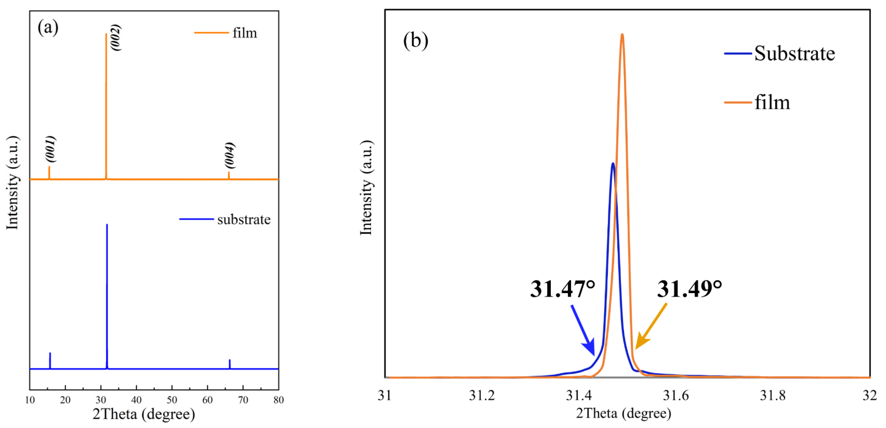
The crystal structure of the films was characterized by XRD. Figure 1a shows the XRD 2theta-omega patterns of the film. The diffraction patterns of the film include only sharp (001), (002), and (004) diffraction peaks, which are almost identical to those of the substrate. It indicates the existence of pure β-Ga2O3 and a single preferred growth orientation along the <001> direction. Figure 1b shows the 2theta-omega patterns of (002) diffraction plane. It is worth noting that the diffraction peak of the film’s (002) diffraction plane has moved to a high angle compared to the substrate. The diffraction plane spacings can be calculated by the Bragg diffraction equation:
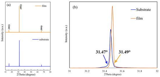
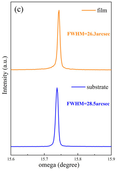
Figure 1.
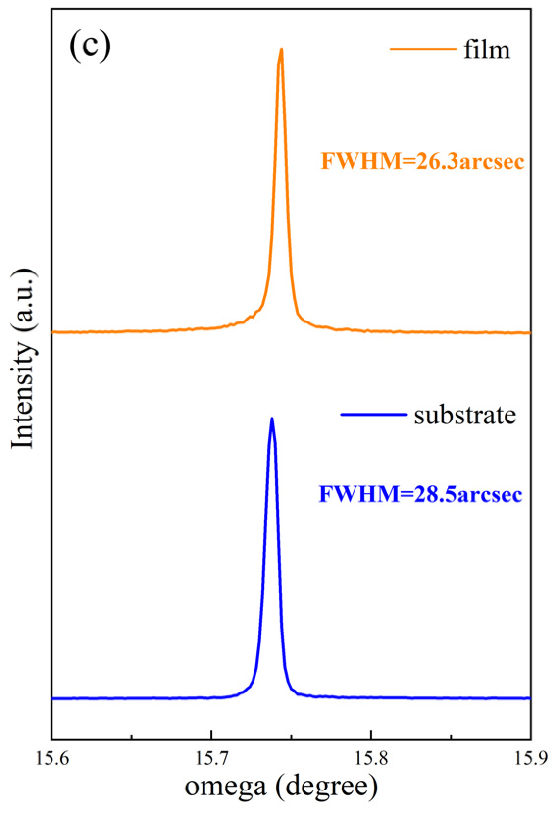
XRD patterns of β-Ga2O3 substrate and film; (a) 2theta-omega patterns in the range of 10°~80°; (b) 2theta-omega patterns of (002) diffraction plane; (c) rocking curve of (002) diffraction plane.
In Equation (1), d is the diffraction plane spacing, λ is the X-ray wavelength (1.54 Å), and θ is the diffraction angle. It was calculated that the (002) diffraction plane spacings of the film and the substrate are 2.839 Å and 2.841 Å. The lattice constant c can be obtained by:
The c values of the film and substrate are and , respectively, basically consistent with the standard lattice constant of β-Ga2O3 (). Assuming the volume conservation of the unit cells, the lattice constant a/b of the film will be smaller than that of the substrate, resulting in two-dimensional tension of the film at the interface. The shrinkage of the lattice was caused by the substitution of Si atoms (radius = 0.41 Å) for Ga atoms (radius = 0.62 Å). The rocking curve of the (002) diffraction plane is shown in Figure 1c. The full width at half maximum (FWHM) of the film is 26.3 arcsec, which is slightly lower than the 28.5 arcsec of the substrate, suggesting a smaller divergence angle and a better orientation of crystal planes. In addition, the dislocation density can be roughly calculated by the following relation [23]:
where B is the diffraction peak FWHM, D is the dislocation density, and b is the Burgers vector. The magnitude of the Burgers vector is about −10, resulting in a dislocation density of 105~106 cm−2, which was comparable to those of the substrate. The FWHM of β-Ga2O3 films prepared by MOCVD is smaller, compared to 27.4 arcsec by HVPE [24], 47.0 arcsec by low-pressure chemical vapor deposition (LPCVD) [25], and 38.9 arcsec by mist-CVD [13], implying a lower dislocation density.
3.2. Raman Analysis
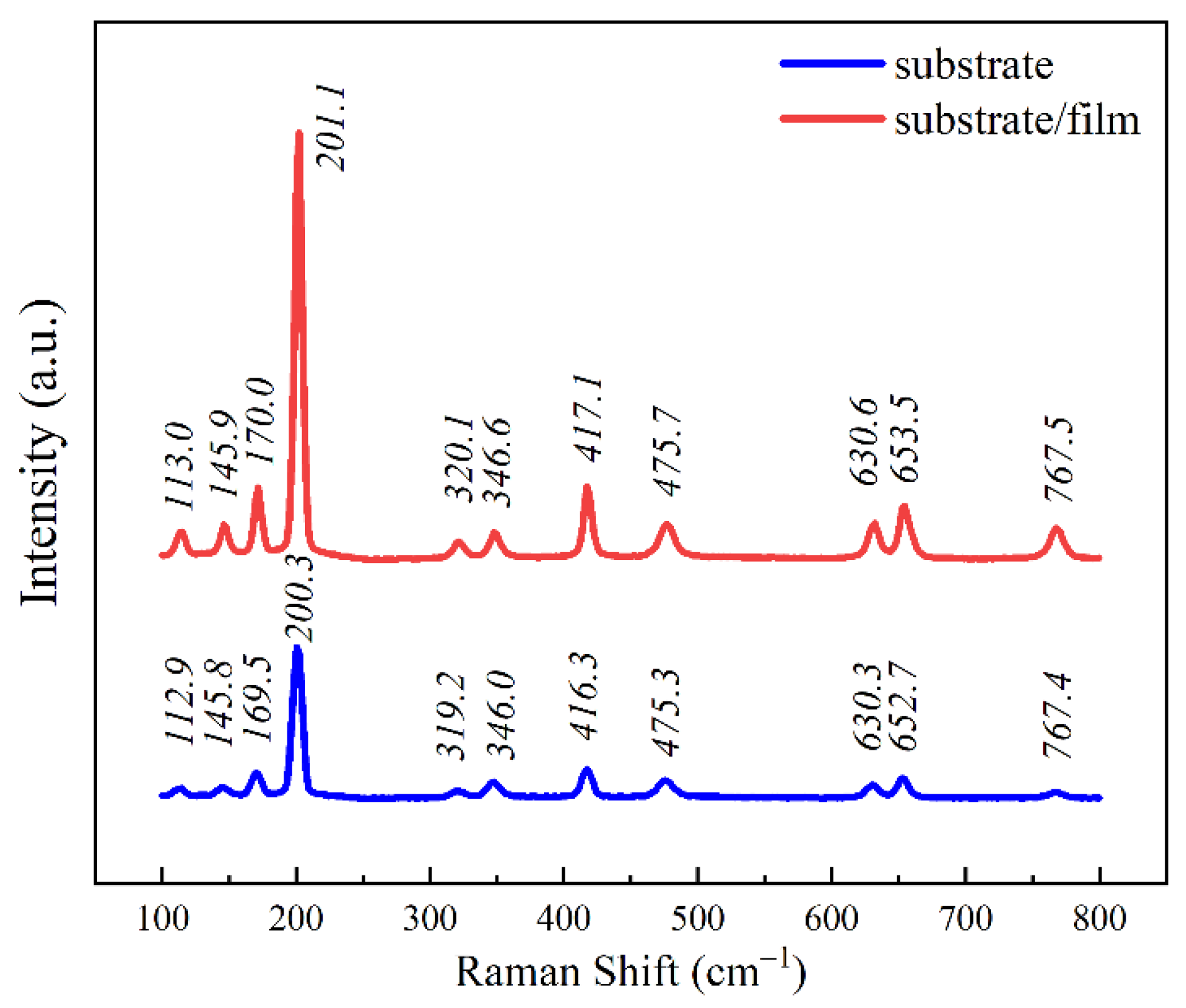
The Ga2O3 film was further investigated with Raman spectra. Before the measurement, the silicon substrate was first used for calibration. Figure 2 shows the Raman spectra of the substrate and the substrate/film template, respectively. There are 15 active vibration modes in Ga2O3 [26]. In Figure 2, 11 of the 15 Raman peaks can be observed. Among them, the Raman peaks in the range of 100–300 cm−1 correspond to the translation and rotation of the Ga-O chain. The Raman peaks of 300–500 cm−1 are derived from the bending vibration of GaⅠ(OⅠ)2 octahedron, whereas the stretching and bending of GaⅠO4 correlate to the Raman peak in the region of 600–800 cm−1. The intensity of all Raman peaks of the template is increased as compared to the substrate. Among them, the FWHM of the Raman peak of the template at 200 cm−1 is 6.8 cm−1, lower than the 8.3 cm−1 of the substrate, indicating the improvement of crystallinity quality. In addition, the Raman peaks of the template are slightly blue-shifted compared to the substrate, which is a result of the internal stress in the film [27]. However, the degree of blue shift is slight, suggesting an approximately low stress state of the film, which is consistent with the XRD results.
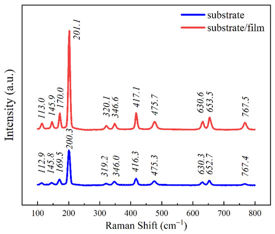
Figure 2.
Raman spectra of Ga2O3 film and substrate.
3.3. Surface Morphological Analysis
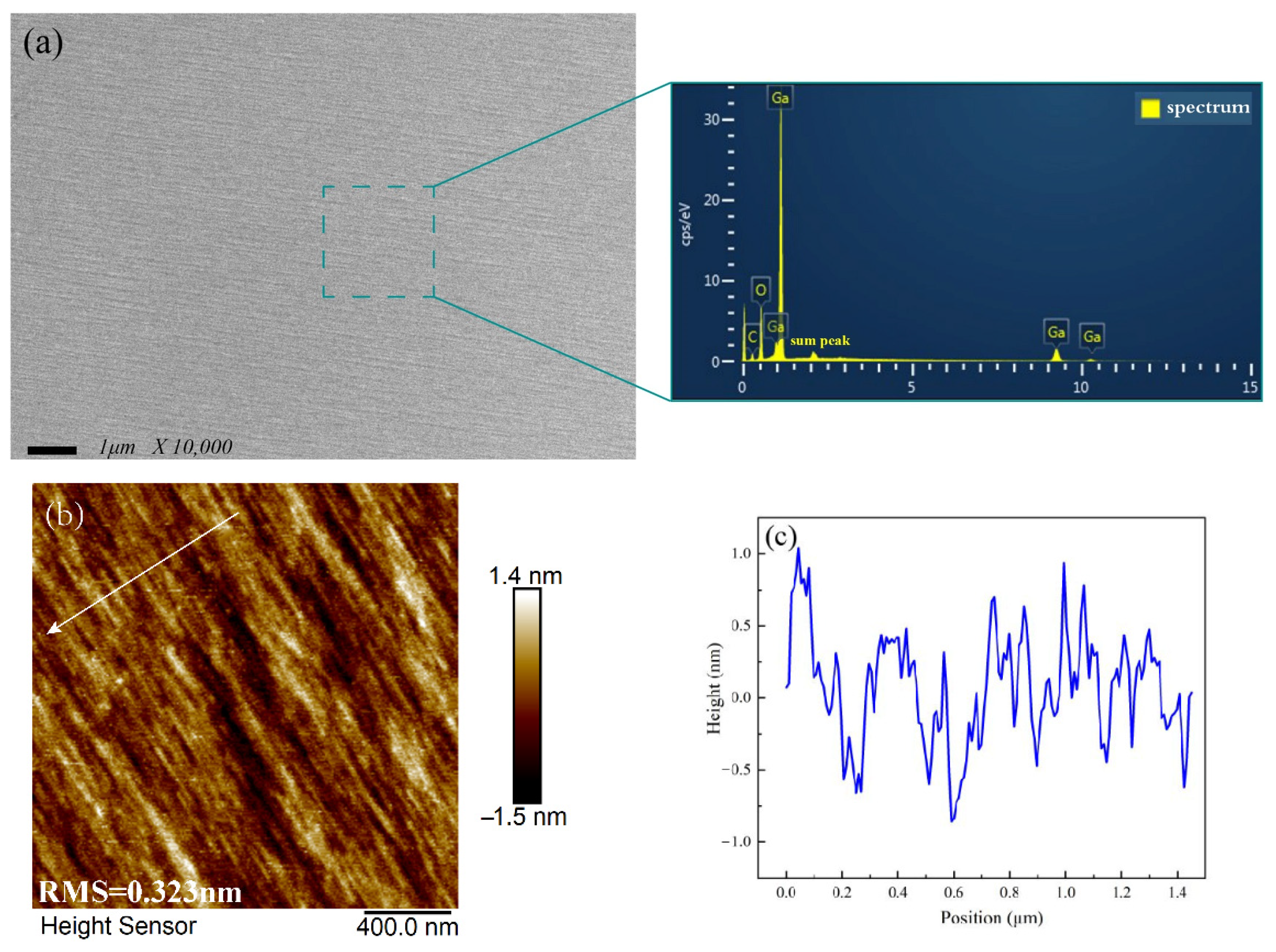
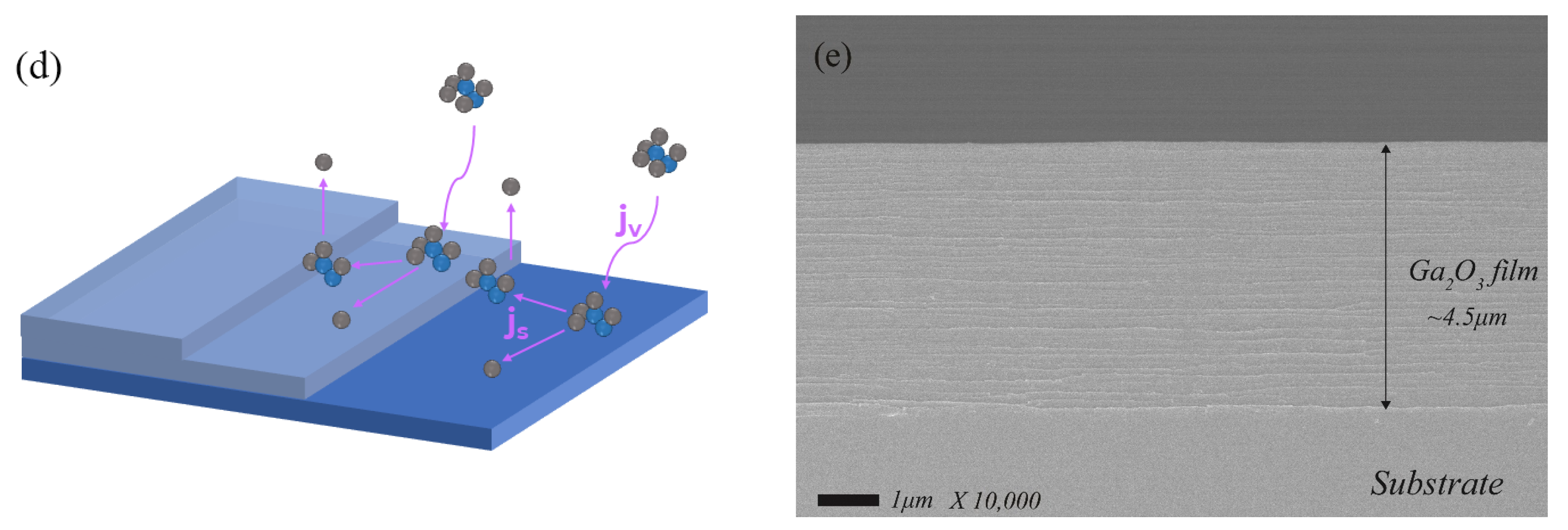
FESEM and AFM were used to examine the surface morphology of the film. The top-view SEM image of the film is shown in Figure 3a. Three elements—carbon, oxygen, and gallium—are detected on the surface with atomic ratios of 17.9%, 47.5%, and 34.6%, respectively, according to the EDX examination of the region within the dashed frame. It is inferred there are two sources of carbon in the films; one is caused by the decomposition of carbon atoms by methyl radicals generated by TMGa at high temperature, and the other is ambient carbon introduced during film measurement and sample preparation. Therefore, a longer growth time will exacerbate carbon fouling, although carbon contamination can be reduced by optimizing the Ⅴ/Ⅲ ratio and gas flow. The AFM picture of the 2 μm × 2 μm region is shown in Figure 3b. The root mean square (RMS) roughness is ~0.3 nm, lower than 1.5 nm by MBE [28], and 7.0 2nm by LPCVD [29]. The height difference between the steps is less than 2 nm, according to the analysis result of the height profile image displayed in Figure 3c. Step flow growth is one of the common growth modes in homoepitaxy, as shown in Figure 3d. Atoms in the fluid are first adsorbed and then diffuse on the mesa. As a result of the lower nucleation work at the step than at the mesa, the molecules will nucleate at the step. A high molecular diffusion speed can lead to the formation of stable step-flow growth modes. The difference in molecular diffusion speed and the morphology of each step layer may cause step bunching. The cross-sectional SEM is shown in Figure 3e. Both the smooth surface and the clear boundary between the substrate and the film can be observed. The film thickness is about 4.5 μm, and the growth rate is estimated to be 1.0 μm/h. In contrast, the growth rate of Ga2O3 films through the mist-CVD is about 3.2 μm/h [13], while the HVPE is as high as 10 μm/h [20].
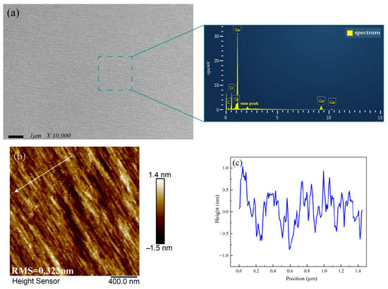

Figure 3.
Image of the single crystalline film; (a) top-view SEM; (b) AFM; (c) height profile along the white arrow in Figure 2b; (d) stages in the process of step flow growth mode; (e) cross-sectional view SEM.
3.4. Elemental Composition Analysis
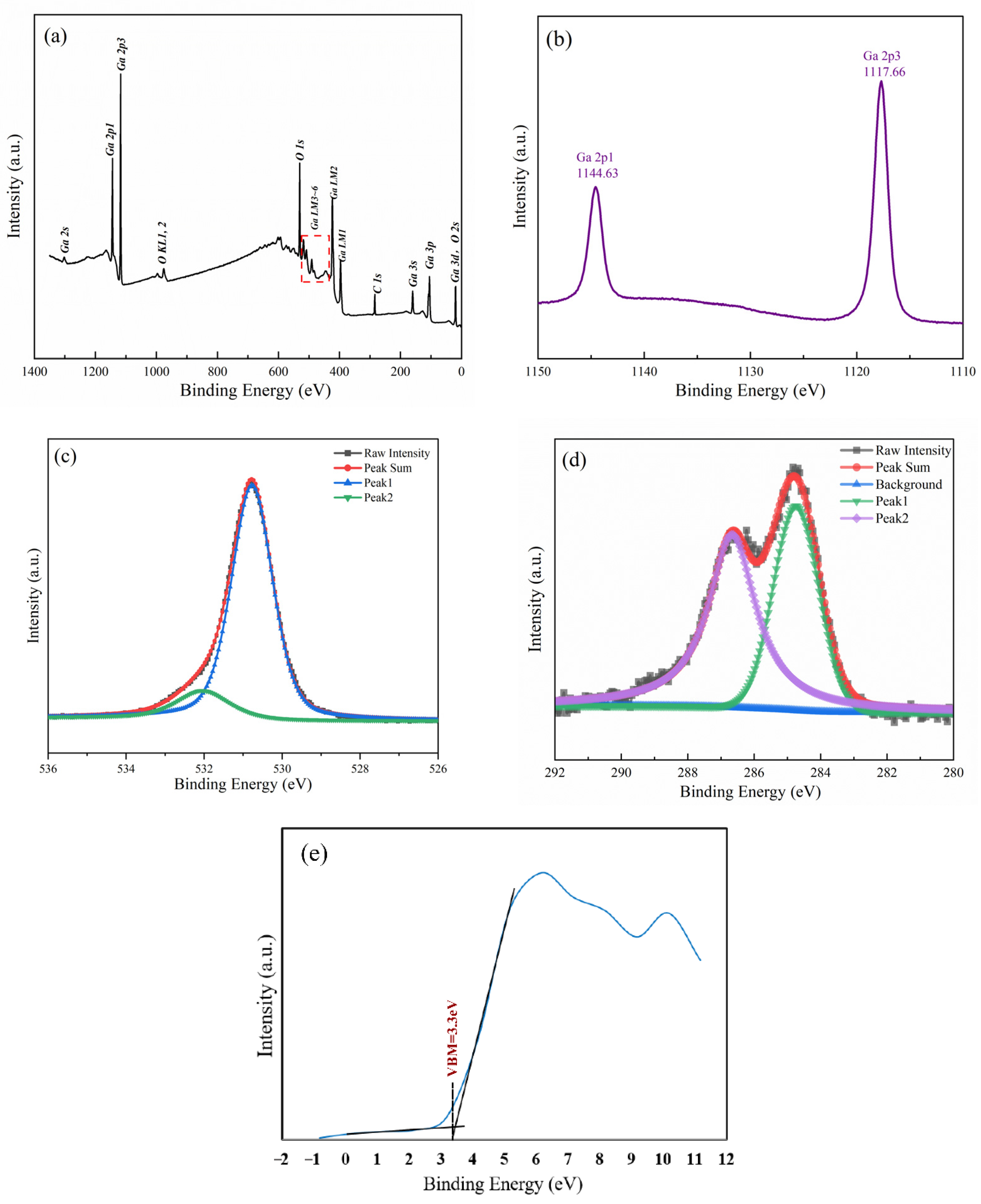
After a pre-sputter, using the Ar+ with an energy of 3 keV, the film was measured by XPS. Figure 4 shows the XPS spectra of the film. The signal peaks of Ga2s, Ga2p, Ga3s, Ga3p, Ga3d, O1s, O2s, and C1s, as well as the Auger electron signal peaks of O and Ga, can be observed in a range from 0 to 1400 eV in Figure 4a. The binding energy was calibrated with the standard value of C1s of 284.8 eV [30,31]. It is found that the carbon element content is 10.3% by the analysis, much lower than that by EDX. This indicates that the surface treatment is beneficial to reduce the contamination from external impurities. Fine spectra were performed on the peaks of Ga2p and O1s. The binding energy peaks of Ga2p are shown in Figure 4b. The binding energies of Ga2p3 and Ga2p1 are 1117.73 eV and 1144.58 eV, which are close to the binding energy of Ga2p [32]. Figure 4c shows the binding energy of O1s. The asymmetric O1s binding energy signal peak can be divided into two peaks by Gaussian fitting. The stronger peak at 530.78 eV is attributed to the Ga2O3 lattice, while the weaker peak at 532.08 eV may be derived from C-O [33,34]. According to the integral area of the two characteristic peaks of Ga2p and O1s and Equation (4), it can be calculated that the ratio of O and Ga atoms is approximately 1.46, which has a slight deviation from the stoichiometric ratio of O and Ga atoms in pure Ga2O3.
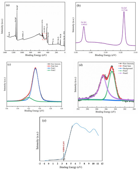
Figure 4.
XPS spectra of the film. (a) general scan; (b) Ga2p core level; (c) raw and fitting spectra of O1s core levels; (d) raw and fitting spectra of C1s core levels; (e) valence band edge spectrum.
In Equation (4), R is the atomic ratio, A is the integral area of the characteristic peak, and S is the sensitivity factor of the corresponding characteristic peak. To clarify the state of carbon in the film, the C1s peak was scanned precisely, as shown in Figure 4d. It can be observed that the C1s peak can be fitted to two peaks with the extreme point at 284.7 eV and 286.8 eV, which may be attributed to C-H and C-O, respectively. This indicates that partial carbon elements exist in the form of C-O, consistent with O1s peak analysis, while another part of the carbon elements originates from C-H, which is probably related to other by-reaction products. Therefore, if the film surface is completely cleaned, there are two sources of carbon contamination in the film, C-O and C-H. In addition, the valence band edge was measured to estimate the Fermi level, as shown in Figure 4e. It can be obtained by linear extrapolation that the valence band maximum (VBM) is 3.3 eV higher than the Fermi zero point. Concerning the value of 4.9 eV for the bandgap of Ga2O3, the Fermi level is about 1.6 eV below the conduction band minimum (CBM). Therefore, the film exhibits weak n-type properties, with a low electron concentration.
3.5. Electron Characteristics Analysis
A Hall test was performed on the film with a size of 1 cm × 1 cm by the Van der Pauw method to characterize the electrical properties. Through five repeated measurements, the average and standard error of the electron concentration are determined to be 3.6 × 1016 cm−3 and 4.0 × 1015 cm−3, respectively. The film has an average electron mobility of 137 cm2/V·s, comparable to previous reports [13,25,35,36]. Therefore, the electrical characteristics of the Si-doped film prepared using the MOCVD technique essentially fulfill the criteria for power diode fabrication.
Table 1 shows partial parameters of the current industrially prepared Ga2O3 epitaxial wafer and substrates. Although the growth rate of MOCVD is lower than that of HVPE, it is found that the MOCVD has more advantages in optimizing the quality and electrical properties of films, which is helpful for the preparation of various devices and the improvement of device performance. Increasing the MOCVD growth rate of Ga2O3 films is the main direction for our next work.

Table 1.
Parameters of Ga2O3 substrates and epitaxial wafers.
4. Conclusions
In summary, the homoepitaxial n-Ga2O3 film with a thickness of 4.5 μm and an electron concentration of 3.6 × 1016 cm−3 was prepared by MOCVD. The XRD confirmed the existence of pure β-Ga2O3 and high crystalline quality of the film. The film surface exhibited a uniform and uniformly oriented step-flow growth mode. The ratio of O atoms to Ga atoms on the film surface was 1.46, close to the stoichiometric ratio of 1.5. The Raman spectra results of the film are consistent with the symmetry of β-Ga2O3. Moreover, it was found that the film was approximately in a stress-free state through analysis and calculation. Si-doped n−-type homoepitaxial Ga2O3 film with a high thickness and high crystal quality was obtained, which offers an effective method to fabricate the Ga2O3-based SBDs and HJDs.
Author Contributions
Conceptualization, C.Z. and T.J.; methodology, W.C.; software, T.J.; validation, W.C.; formal analysis, Z.L. (Zeming Li) and Z.D.; investigation, B.Z.; data curation, Y.Z.; writing—original draft preparation, C.Z. and T.J.; writing—review and editing, X.D.; visualization, Z.L. (Zhengda Li); supervision, X.D.; project administration, X.D. and G.D.; funding acquisition, X.D. All authors have read and agreed to the published version of the manuscript.
Funding
This research was funded by the National Natural Science Foundation of China, grant numbers 61774072: 61734001, 61574069, and 61674068; the National Key Research and Development Program, grant number 2018YFB0406703; the National Natural Science Foundation of China, Grant Numbers 62074069, 61734001 and 61674068; and the Science and Technology Developing Project of Jilin Province, grant number 20200801013GH.
Institutional Review Board Statement
Not applicable.
Informed Consent Statement
Not applicable.
Data Availability Statement
The data are contained within the article.
Conflicts of Interest
The authors declare no conflict of interest.
References
- Pearton, S.J.; Yang, J.C.; Cary, P.H.; Ren, F.; Kim, J.; Tadjer, M.J.; Mastro, M.A. A review of Ga2O3 materials, processing, and devices. Appl Phys. Rev. 2018, 5, 011301. [Google Scholar] [CrossRef] [Green Version]
- Razeghi, M.; Park, J.H.; McClintock, R.; Pavlidis, D.; Teherani, F.H.; Rogers, D.J.; Magill, B.A.; Khodaparast, G.A.; Xu, Y.B.; Wu, J.S.; et al. A Review of the Growth, Doping & Applications of beta-Ga2O3 thin films. Proc. Spie 2018, 10533, 21–44. [Google Scholar] [CrossRef]
- Tang, X.; Li, K.H.; Zhao, Y.; Sui, Y.X.; Liang, H.L.; Liu, Z.; Liao, C.H.; Babatain, W.Y.; Lin, R.Y.; Wang, C.J.; et al. Quasi-epitaxial growth of β-Ga2O3-coated wide band gap semiconductor tape for flexible UV photodetectors. ACS Appl. Mater. Interfaces 2021, 14, 1304–1314. [Google Scholar] [CrossRef] [PubMed]
- Higashiwaki, M.; Murakami, H.; Kumagai, Y.; Kuramata, A. Current status of Ga2O3 power devices. Jpn J. Appl. Phys. 2016, 55, 1202A1. [Google Scholar] [CrossRef]
- Konishi, K.; Goto, K.; Murakami, H.; Kumagai, Y.; Kuramata, A.; Yamakoshi, S.; Higashiwaki, M. 1-kV vertical Ga2O3 field-plated Schottky barrier diodes. Appl. Phys. Lett. 2017, 110, 103506. [Google Scholar] [CrossRef]
- Hoshikawa, K.; Ohba, E.; Kobayashi, T.; Yanagisawa, J.; Miyagawa, C.; Nakamura, Y. Growth of beta-Ga2O3 single crystals using vertical Bridgman method in ambient air. J. Cryst. Growth 2016, 447, 36–41. [Google Scholar] [CrossRef]
- Maslov, V.N.; Krymov, V.M.; Blashenkov, M.N.; Golovatenko, A.A.; Nikolaev, V.I. beta-Ga2O3 crystal growing from its own melt. Tech. Phys. Lett. 2014, 40, 303–305. [Google Scholar] [CrossRef]
- Tomm, Y.; Reiche, P.; Klimm, D.; Fukuda, T. Czochralski grown Ga2O3 crystals. J. Cryst Growth 2000, 220, 510–514. [Google Scholar] [CrossRef]
- Xu, W.L.; Shi, J.C.; Li, Y.W.; Xiu, X.Q.; Ding, S.; Xie, Z.L.; Tao, T.; Chen, P.; Liu, B.; Zhang, R.; et al. Study of β-Ga2O3 films hetero-epitaxially grown on off-angled sapphire substrates by halide vapor phase epitaxy. Mater. Lett. 2021, 289, 129411. [Google Scholar] [CrossRef]
- Kidalov, V.V.; Dyadenchuk, A.F.; Kladko, V.P.; Gudymenko, O.I.; Derhachov, M.P.; Popov, S.O.; Sushko, O.O.; Kidalov, V.V. Structure and electrical properties of β-Ga2O3 films obtained by radio frequency magnetron sputtering on porous silicon. ECS J. Solid State Sc. 2022, 11, 025004. [Google Scholar] [CrossRef]
- Jiao, T.; Li, Z.M.; Chen, W.; Dong, X.; Li, Z.D.; Diao, Z.T.; Zhang, Y.T.; Zhang, B.L. Stable electron concentration Si-doped β-Ga2O3 films homoepitaxial growth by MOCVD. Coatings 2021, 11, 589. [Google Scholar] [CrossRef]
- Li, Z.M.; Jiao, T.; Hu, D.Q.; Lv, Y.J.; Li, W.C.; Dong, X.; Zhang, Y.T.; Feng, Z.H.; Zhang, B.L. Study on β-Ga2O3 films grown with various VI/III ratios by MOCVD. Coatings 2019, 9, 281. [Google Scholar] [CrossRef] [Green Version]
- Nishinaka, H.; Nagaoka, T.; Kajita, Y.; Yoshimoto, M. Rapid homoepitaxial growth of (010) β-Ga2O3 thin films via mist chemical vapor deposition. Mater. Sci. Semicond. Process. 2021, 128, 105732. [Google Scholar] [CrossRef]
- Vogt, P.; Hensling, F.; Azizie, K.; Chang, C.S.; Schlom, D.G. Adsorption-controlled growth of Ga2O3 by suboxide molecular-beam epitaxy. APL Mater. 2021, 9, 031101. [Google Scholar] [CrossRef]
- Ghosh, S.; Baral, M.; Kamparath, R.; Choudhary, R.J.; Phase, D.M.; Singh, S.D.; Ganguli, T. Epitaxial growth and interface band alignment studies of all oxide alpha-Cr2O3/beta-Ga2O3 p-n heterojunction. Appl. Phys. Lett. 2019, 115, 061602. [Google Scholar] [CrossRef]
- Kan, S.; Takemoto, S.; Kaneko, K.; Takahashi, I.; Sugimoto, M.; Shinohe, T.; Fujita, S. Electrical properties of alpha-Ir2O3/alpha-Ga2O3 pn heterojunction diode and band alignment of the heterostructure. Appl. Phys. Lett. 2018, 113, 212104. [Google Scholar] [CrossRef]
- Watahiki, T.; Yuda, Y.; Furukawa, A.; Yamamuka, M.; Takiguchi, Y.; Miyajima, S. Heterojunction p-Cu2O/n-Ga2O3 diode with high breakdown voltage. Appl. Phys. Lett. 2017, 111, 222104. [Google Scholar] [CrossRef]
- Ji, M.; Taylor, N.R.; Kravchenko, I.; Joshi, P.; Aytug, T.; Cao, L.R.; Paranthaman, M.P. Demonstration of Large-Size Vertical Ga2O3 Schottky Barrier Diodes. IEEE Trans. Power Electr. 2021, 36, 41–44. [Google Scholar] [CrossRef]
- Wang, Y.G.; Cai, S.J.; Liu, M.; Lv, Y.J.; Long, S.B.; Zhou, X.Y.; Song, X.B.; Liang, S.X.; Han, T.T.; Tan, X.; et al. High-Voltage ((2)over-bar01) beta-Ga2O3 Vertical Schottky Barrier Diode With Thermally-Oxidized Termination. IEEE Electr. Device L 2020, 41, 131–134. [Google Scholar] [CrossRef]
- Higashiwaki, M.; Sasaki, K.; Goto, K.; Nomura, K.; Thieu, Q.T.; Togashi, R.; Murakami, H.; Kumagai, Y.; Monemar, B.; Koukitu, A.; et al. Ga2O3 Schottky Barrier Diodes with n(-)-Ga2O3 Drift Layers Grown by HVPE. In Proceedings of the 2015 73rd Annual Device Research Conference (DRC), Columbus, OH, USA, 21–24 June 2015; pp. 29–30. [Google Scholar]
- Li, Z.M.; Jiao, T.; Yu, J.Q.; Hu, D.Q.; Lv, Y.J.; Li, W.C.; Dong, X.; Zhang, B.L.; Zhang, Y.T.; Feng, Z.H.; et al. Single crystalline beta-Ga2O3 homoepitaxial films grown by MOCVD. Vacuum 2020, 178, 109440. [Google Scholar] [CrossRef]
- Farzana, E.; Alema, F.; Ho, W.Y.; Mauze, A.; Itoh, T.; Osinsky, A.; Speck, J.S. Vertical beta-Ga2O3 field plate Schottky barrier diode from metal-organic chemical vapor deposition. Appl. Phys. Lett. 2021, 118, 162109. [Google Scholar] [CrossRef]
- Gay, P.; Hirsch, P.B.; Kelly, A. The estimation of dislocation densities in metals from X-ray data. Acta Metall. 1953, 1, 315–319. [Google Scholar] [CrossRef]
- Leach, J.H.; Udwary, K.; Rumsey, J.; Dodson, G.; Splawn, H.; Evans, K.R. Halide vapor phase epitaxial growth of beta-Ga2O3 and alpha-Ga2O3 films. APL Mater. 2019, 7, 022504. [Google Scholar] [CrossRef] [Green Version]
- Rafique, S.; Karim, M.R.; Johnson, J.M.; Hwang, J.; Zhao, H.P. LPCVD homoepitaxy of Si doped beta-Ga2O3 thin films on (010) and (001) substrates. Appl. Phys. Lett. 2018, 112, 052104. [Google Scholar] [CrossRef] [Green Version]
- Dohy, D.; Lucaz Ea, U.G.; Revcolevschi, A. Raman spectra and valence force field of single-crystalline β Ga2O3. J. Solid State Chem. 1982, 45, 180–192. [Google Scholar] [CrossRef]
- Zhang, S.L.; Zhu, B.F.; Huang, F.M.; Yan, Y.; Shang, E.Y.; Fan, S.S.; Han, W.G. Effect of defects on optical phonon Raman spectra in SiC nanorods. Solid State Commun. 1999, 111, 647–651. [Google Scholar] [CrossRef]
- Tellekamp, M.B.; Heinselman, K.N.; Harvey, S.; Khan, I.S.; Zakutayev, A. Growth and characterization of homoepitaxial beta-Ga(2)O(3)layers. J. Phys. D-Appl. Phys. 2020, 53, 484002. [Google Scholar] [CrossRef]
- Rafique, S.; Han, L.; Tadjer, M.J.; Freitas, J.A.; Mahadik, N.A.; Zhao, H.P. Homoepitaxial growth of beta-Ga2O3 thin films by low pressure chemical vapor deposition. Appl. Phys. Lett. 2016, 108, 182105. [Google Scholar] [CrossRef]
- Greczynski, G.; Hultman, L. Compromising Science by Ignorant Instrument Calibration-Need to Revisit Half a Century of Published XPS Data. Angew. Chem. Int. Ed. 2020, 59, 5002–5006. [Google Scholar] [CrossRef]
- Greczynski, G.; Hultman, L. Reliable determination of chemical state in x-ray photoelectron spectroscopy based on sample-work-function referencing to adventitious carbon: Resolving the myth of apparent constant binding energy of the C 1s peak. Appl. Surf. Sci. 2018, 451, 99–103. [Google Scholar] [CrossRef]
- Mi, W.; Du, X.J.; Luan, C.N.; Xiao, H.D.; Ma, J. Electrical and optical characterizations of beta-Ga2O3: Sn films deposited on MgO(110) substrate by MOCVD. Rsc Adv. 2014, 4, 30579–30583. [Google Scholar] [CrossRef]
- Chen, M.; Wang, X.; Yu, Y.H.; Pei, Z.L.; Bai, X.D.; Sun, C.; Huang, R.F.; Wen, L.S. X-ray photoelectron spectroscopy and auger electron spectroscopy studies of Al-doped ZnO films. Appl. Surf. Sci. 2000, 158, 134–140. [Google Scholar] [CrossRef]
- Ma, Y.J.; Feng, B.Y.; Zhang, X.D.; Chen, T.W.; Tang, W.B.; Zhang, L.; He, T.; Zhou, X.; Wei, X.; Fu, H.Q.; et al. High-performance beta-Ga2O3 solar-blind ultraviolet photodetectors epitaxially grown on (110) TiO2 substrates by metalorganic chemical vapor deposition. Vacuum 2021, 191, 110402. [Google Scholar] [CrossRef]
- Goto, K.; Konishi, K.; Murakami, H.; Kumagai, Y.; Monemar, B.; Higashiwaki, M.; Kuramata, A.; Yamakoshi, S. Halide vapor phase epitaxy of Si doped beta-Ga2O3 and its electrical properties. Thin Solid Film 2018, 666, 182–184. [Google Scholar] [CrossRef]
- Baldini, M.; Albrecht, M.; Fiedler, A.; Irmscher, K.; Schewski, R.; Wagner, G. Si- and Sn-Doped Homoepitaxial beta-Ga2O3 Layers Grown by MOVPE on (010)-Oriented Substrates. ECS J. Solid State Sci. Technol. 2017, 6, Q3040–Q3044. [Google Scholar] [CrossRef]
- Huang, S.; Lopez, R.; Paul, S.; Neal, A.T.; Mou, S.; Houng, M.P.; Li, J.V. β-Ga2O3 defect study by steady-state capacitance spectroscopy. Jpn. J. Appl. Phys. 2018, 57, 091101. [Google Scholar] [CrossRef]
- Aida, H.; Nishiguchi, K.; Takeda, H.; Aota, N.; Sunakawa, K.; Yaguchi, Y. Growth of β-Ga2O3 single crystals by the edge-defined, film fed growth method. Jpn. J. Appl. Phys. 2008, 47, 8506. [Google Scholar] [CrossRef]
- Thieu, Q.T.; Wakimoto, D.; Koishikawa, Y.; Sasaki, K.; Goto, K.; Konishi, K.; Murakami, H.; Kuramata, A.; Kumagai, Y.; Yamakoshi, S. Preparation of 2-in.-diameter (001) β-Ga2O3 homoepitaxial wafers by halide vapor phase epitaxy. Jpn. J. Appl. Phys. 2017, 56, 110310. [Google Scholar] [CrossRef]
Publisher’s Note: MDPI stays neutral with regard to jurisdictional claims in published maps and institutional affiliations. |
© 2022 by the authors. Licensee MDPI, Basel, Switzerland. This article is an open access article distributed under the terms and conditions of the Creative Commons Attribution (CC BY) license (https://creativecommons.org/licenses/by/4.0/).