
Low-Temperature CVD-Grown Graphene Thin Films as Transparent Electrode for Organic Photovoltaics

 ,
,  , , , and
Abstract
:1. Introduction
2. Experimental Procedure
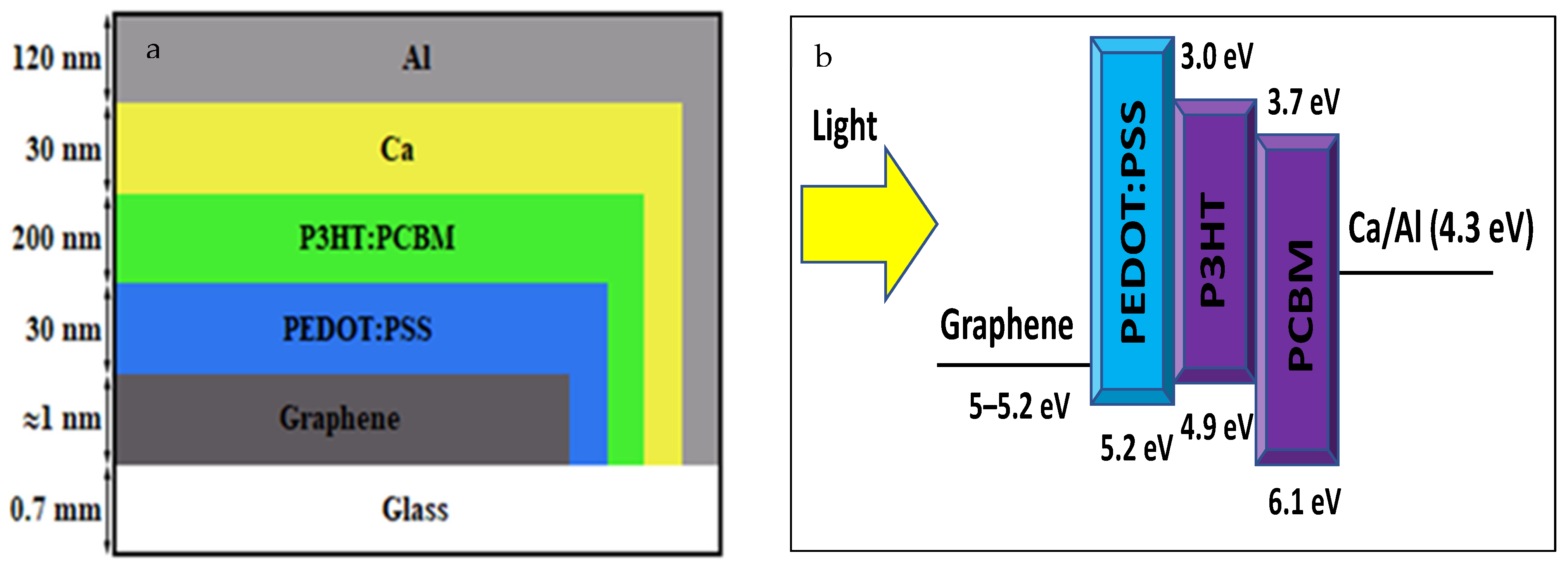
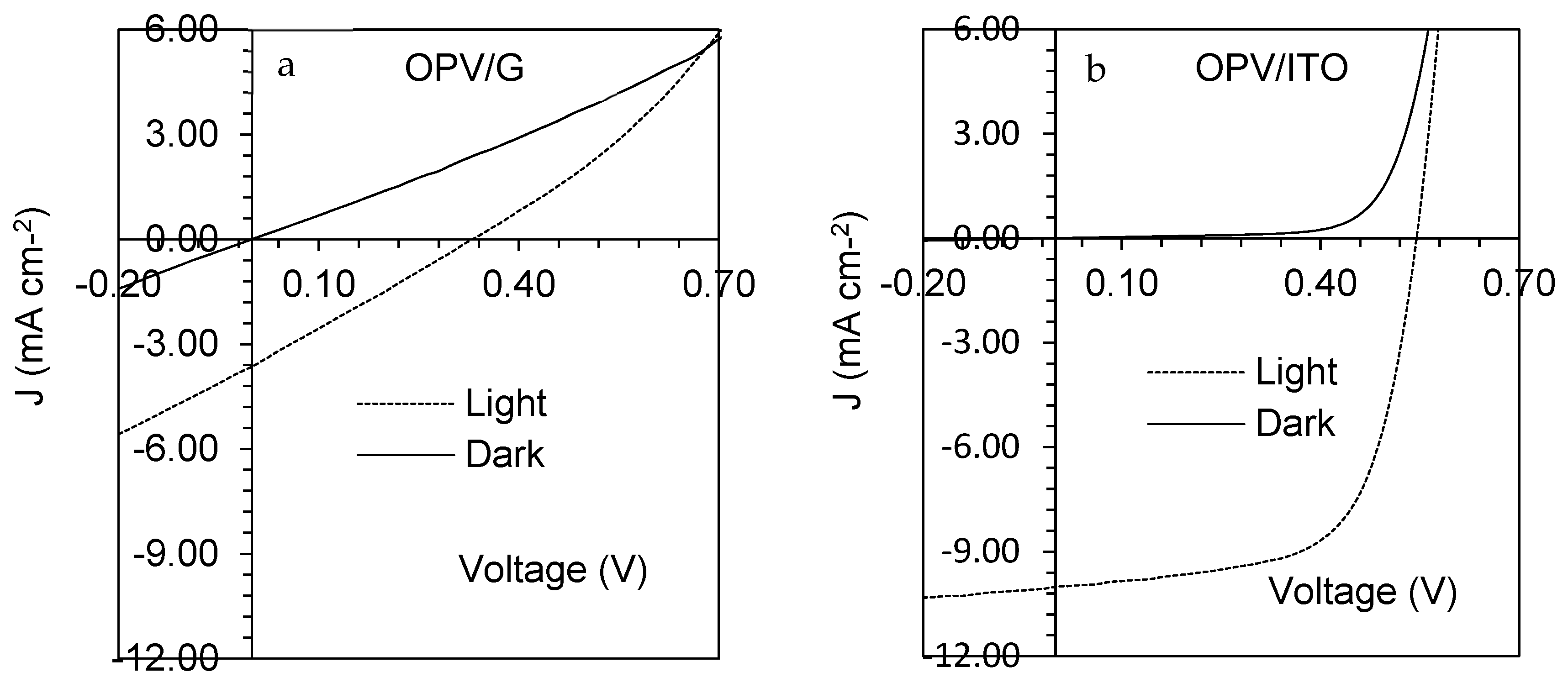
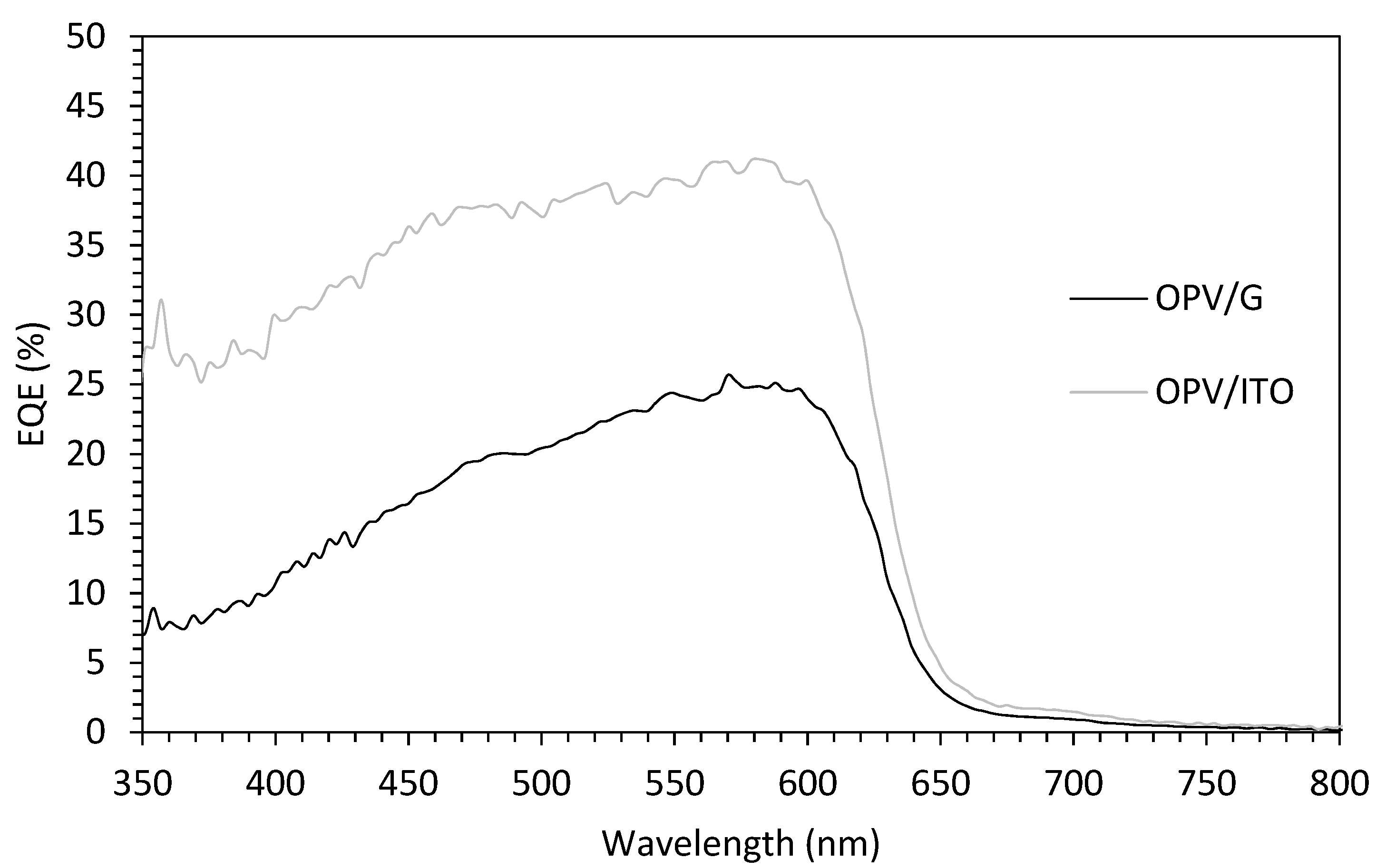
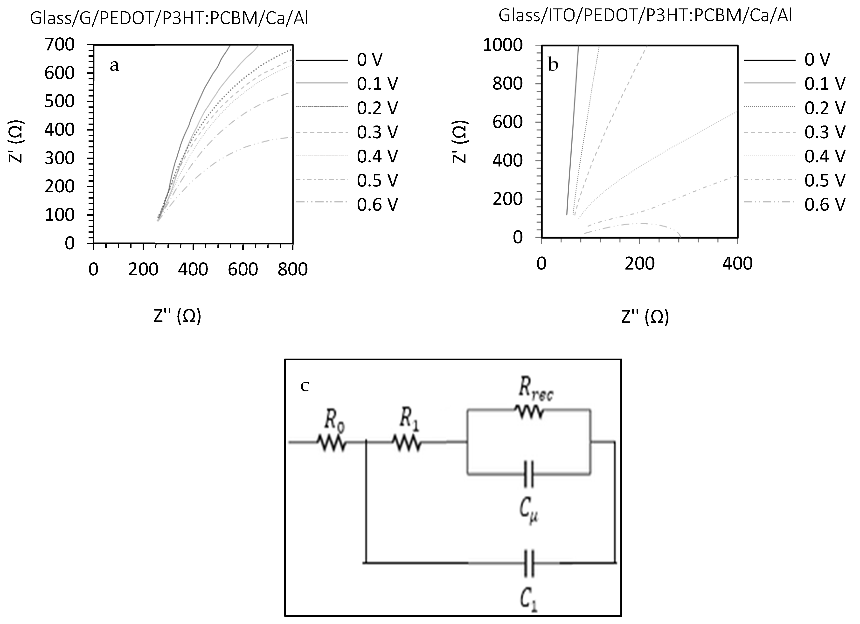
3. Results and Discussion
4. Conclusions
Supplementary Materials
Author Contributions
Funding
Institutional Review Board Statement
Informed Consent Statement
Data Availability Statement
Acknowledgments
Conflicts of Interest
References
- Geim, A.K.; Novoselov, K.S. The rise of graphene. Nat. Mater. 2007, 6, 183–191. [Google Scholar] [CrossRef] [PubMed]
- Castro Neto, A.H.; Peres, N.M.R.; Novoselov, K.S.; Geim, A.K. The electronic properties of graphene. Rev. Mod. Phys. 2009, 81, 109–162. [Google Scholar] [CrossRef] [Green Version]
- Novoselov, K.S.; Geim, A.K.; Morozov, S.V.; Jiang, D.; Zhang, Y.; Dubonos, S.V.; Grigorieva, I.V.; Firsov, A.A. Electric field effect in atomically thin carbon films. Science 2004, 306, 666–669. [Google Scholar] [CrossRef] [PubMed] [Green Version]
- Balandin, A.A.; Ghosh, S.; Bao, W.; Calizo, I.; Teweldebrhan, D.; Miao, F.; Lau, C.N. Superior thermal conductivity of single-layer graphene. Nano Lett. 2008, 8, 902–907. [Google Scholar] [CrossRef] [PubMed]
- Lee, C.; Wei, X.; Kysar, J.W.; Hone, J. Measurement of the elastic properties and intrinsic strength of monolayer graphene. Science 2008, 321, 385–388. [Google Scholar] [CrossRef] [PubMed]
- Nair, R.R.; Blake, P.; Grigorenko, A.N.; Novoselov, K.S.; Booth, T.J.; Stauber, T.; Peres, N.M.; Geim, A.K. Fine structure constant defines visual transparency of graphene. Science 2008, 320, 1308. [Google Scholar] [CrossRef] [PubMed] [Green Version]
- Wang, Y.; Chen, X.; Zhong, Y.; Zhu, F.; Loh, K.P. Large area, continuous, few-layered graphene as anodes in organic photovoltaic devices. Appl. Phys. Lett. 2009, 95, 063302. [Google Scholar] [CrossRef]
- Hyesung, P.; Jill, A.R.; Ki Kang, K.; Vladimir, B.; Jing, K. Doped graphene electrodes for organic solar cells. Nanotechnology 2010, 21, 505204. [Google Scholar]
- Gomez De Arco, L.; Zhang, Y.; Schlenker, C.W.; Ryu, K.; Thompson, M.E.; Zhou, C. Continuous, highly flexible, and transparent graphene films by chemical vapor deposition for organic photovoltaics. ACS Nano 2010, 4, 2865–2873. [Google Scholar] [CrossRef]
- Wang, Y.; Tong, S.W.; Xu, X.F.; Özyilmaz, B.; Loh, K.P. Interface engineering of layer-by-layer stacked graphene anodes for high-performance organic solar cells. Adv. Mater. 2011, 23, 1514–1518. [Google Scholar] [CrossRef]
- Park, H.; Brown, P.R.; Bulović, V.; Kong, J. Graphene as transparent conducting electrodes in organic photovoltaics: Studies in graphene morphology, hole transporting layers, and counter electrodes. Nano Lett. 2012, 12, 133–140. [Google Scholar] [CrossRef] [PubMed]
- Zhang, Q.; Wan, X.; Xing, F.; Huang, L.; Long, G.; Yi, N.; Ni, W.; Liu, Z.; Tian, J.; Chen, Y. Solution-processable graphene mesh transparent electrodes for organic solar cells. Nano Res. 2013, 6, 478–484. [Google Scholar] [CrossRef]
- Park, H.; Chang, S.; Smith, M.; Gradečak, S.; Kong, J. Interface engineering of graphene for universal applications as both anode and cathode in organic photovoltaics. Sci. Rep. 2013, 3, 1581. [Google Scholar] [CrossRef] [PubMed] [Green Version]
- Hobeom, K.; Sang-Hoon, B.; Tae-Hee, H.; Kyung-Geun, L.; Jong-Hyun, A.; Tae-Woo, L. Organic solar cells using CVD-grown graphene electrodes. Nanotechnology 2014, 25, 014012. [Google Scholar]
- Wang, X.; Zhi, L.; Müllen, K. Transparent, conductive graphene electrodes for dye-sensitized solar cells. Nano Lett. 2008, 8, 323–327. [Google Scholar] [CrossRef]
- Wang, X.; Zhi, L.; Tsao, N.; Tomovic, Z.; Li, J.; Mullen, K. Transparent carbon films as electrodes in organic solar cells. Angew. Chem. Int. Ed. Engl. 2008, 47, 2990–2992. [Google Scholar] [CrossRef]
- Li, X.; Cai, W.; An, J.; Kim, S.; Nah, J.; Yang, D.; Piner, R.; Velamakanni, A.; Jung, I.; Tutuc, E.; et al. Large-area synthesis of high-quality and uniform graphene films on copper foils. Science 2009, 324, 1312–1314. [Google Scholar] [CrossRef] [Green Version]
- Bae, S.; Kim, H.; Lee, Y.; Xu, X.; Park, J.-S.; Zheng, Y.; Balakrishnan, J.; Lei, T.; Ri Kim, H.; Song, Y.I.; et al. Roll-to-roll production of 30-inch graphene films for transparent electrodes. Nat. Nanotechnol. 2010, 5, 574–578. [Google Scholar] [CrossRef] [Green Version]
- Kim, K.S.; Zhao, Y.; Jang, H.; Lee, S.Y.; Kim, J.M.; Kim, K.S.; Ahn, J.H.; Kim, P.; Choi, J.Y.; Hong, B.H. Large-scale pattern growth of graphene films for stretchable transparent electrodes. Nature 2009, 457, 706–710. [Google Scholar] [CrossRef]
- Reina, A.; Jia, X.; Ho, J.; Nezich, D.; Son, H.; Bulovic, V.; Dresselhaus, M.S.; Kong, J. Large area, few-layer graphene films on arbitrary substrates by chemical vapor deposition. Nano Lett. 2009, 9, 30–35. [Google Scholar] [CrossRef]
- Ago, H.; Ito, Y.; Mizuta, N.; Yoshida, K.; Hu, B.; Orofeo, C.M.; Tsuji, M.; Ikeda, K.-I.; Mizuno, S. Epitaxial chemical vapor deposition growth of single-layer graphene over cobalt film crystallized on sapphire. ACS Nano 2010, 4, 7407–7414. [Google Scholar] [CrossRef] [PubMed]
- Miyata, Y.; Kamon, K.; Ohashi, K.; Kitaura, R.; Yoshimura, M.; Shinohara, H. A simple alcohol-chemical vapor deposition synthesis of single-layer graphenes using flash cooling. Appl. Phys. Lett. 2010, 96, 263105. [Google Scholar] [CrossRef]
- Li, Z.; Wu, P.; Wang, C.; Fan, X.; Zhang, W.; Zhai, X.; Zeng, C.; Li, Z.; Yang, J.; Hou, J. Low-temperature growth of graphene by chemical vapor deposition using solid and liquid carbon sources. ACS Nano 2011, 5, 3385–3390. [Google Scholar] [CrossRef] [PubMed]
- Sun, Z.; Yan, Z.; Yao, J.; Beitler, E.; Zhu, Y.; Tour, J.M. Growth of graphene from solid carbon sources. Nature 2010, 468, 549–552. [Google Scholar] [CrossRef] [PubMed]
- Jaeho Kim, H.S.; Itagaki, H. Low-temperature graphene growth by forced convection of plasma-excited radi-cals. Nano Lett. 2019, 19, 739–746. [Google Scholar]
- Koosha, N.; Karimi-Sabet, J.; Moosavian, M.A.; Amini, Y. Improvement of synthesized graphene structure through various solvent liquids at low temperature by chemical vapor deposition method. Mater. Sci. Eng. B 2021, 274, 115458. [Google Scholar] [CrossRef]
- Yu, Q.; Jauregui, L.A.; Wu, W.; Colby, R.; Tian, J.; Su, Z.; Cao, H.; Liu, Z.; Pandey, D.; Wei, D.; et al. Control and characterization of individual grains and grain boundaries in graphene grown by chemical vapour deposition. Nat. Mater. 2011, 10, 443–449. [Google Scholar] [CrossRef] [Green Version]
- Wu, T.; Ding, G.; Shen, H.; Wang, H.; Sun, L.; Jiang, D.; Xie, X.; Jiang, M. Triggering the continuous growth of graphene toward millimeter-sized grains. Adv. Funct. Mater. 2013, 23, 198–203. [Google Scholar] [CrossRef] [Green Version]
- Chen, S.; Ji, H.; Chou, H.; Li, Q.; Li, H.; Suk, J.W.; Piner, R.; Liao, L.; Cai, W.; Ruoff, R.S. Millimeter-size single-crystal graphene by suppressing evaporative loss of cu during low pressure chemical vapor deposition. Adv. Mater. 2013, 25, 2062–2065. [Google Scholar] [CrossRef]
- Suk, J.W.; Kitt, A.; Magnuson, C.W.; Hao, Y.; Ahmed, S.; An, J.; Swan, A.K.; Goldberg, B.B.; Ruoff, R.S. Transfer of CVD-grown monolayer graphene onto arbitrary substrates. ACS Nano 2011, 5, 6916–6924. [Google Scholar] [CrossRef]
- Song, J.; Kam, F.-Y.; Png, R.-Q.; Seah, W.-L.; Zhuo, J.-M.; Lim, G.-K.; Ho, P.K.H.; Chua, L.-L. A general method for transferring graphene onto soft surfaces. Nat. Nanotechnol. 2013, 8, 356–362. [Google Scholar] [CrossRef] [PubMed]
- Lee, Y.-Y.; Tu, K.-H.; Yu, C.-C.; Li, S.-S.; Hwang, J.-Y.; Lin, C.-C.; Chen, K.-H.; Chen, L.-C.; Chen, H.-L.; Chen, C.-W. Top laminated graphene electrode in a semitransparent polymer solar cell by simultaneous thermal annealing/releasing method. ACS Nano 2011, 5, 6564–6570. [Google Scholar] [CrossRef] [PubMed]
- Cox, M.; Gorodetsky, A.; Kim, B.; Kim, K.S.; Jia, Z.; Kim, P.; Nuckolls, C.; Kymissis, I. Single-layer graphene cathodes for organic photovoltaics. Appl. Phys. Lett. 2011, 98, 123303. [Google Scholar] [CrossRef] [Green Version]
- Rosli, N.N.; Ibrahim, M.A.; Ludin, N.A.; Teridi, M.A.M.; Sopian, K. A review of graphene based transparent conducting films for use in solar photovoltaic applications. Renew. Sustain. Energy Rev. 2019, 99, 83. [Google Scholar] [CrossRef]
- Sulaiman, K.; Ali, A.Y.; Elkington, D.; Feron, K.; Anderson, K.F.; Belcher, W.; Dastoor, P.; Zhou, X. Matrix assisted low temperature growth of graphene. Carbon 2016, 107, 325–331. [Google Scholar] [CrossRef]
- Cooling, N.A.; Barnes, E.F.; Almyahi, F.; Feron, K.; Al-Mudhaffer, M.F.; Al-Ahmad, A.; Vaughan, B.; Andersen, T.R.; Griffith, M.J.; Hart, A.S.; et al. A low-cost mixed fullerene acceptor blend for printed electronics. J. Mater. Chem. A 2016, 4, 10274–10281. [Google Scholar] [CrossRef]
- Ali, A.Y.; Holmes, N.P.; Holdsworth, J.; Belcher, W.; Dastoor, P.; Zhou, X. Growth of multi-layered graphene using organic solvent-pmma film as the carbon source under low temperature conditions. Int. J. Chem. Mater. Eng. 2019, 13, 77–81. [Google Scholar]
- Losurdo, M.; Giangregorio, M.M.; Capezzuto, P.; Bruno, G. Graphene CVD growth on copper and nickel: Role of hydrogen in kinetics and structure. Phys. Chem. Chem. Phys. 2011, 13, 20836–20843. [Google Scholar] [CrossRef]
- Wu, W.; Yu, Q.; Peng, P.; Liu, Z.; Bao, J.; Pei, S.S. Control of thickness uniformity and grain size in graphene films for transparent conductive electrodes. Nanotechnology 2012, 23, 035603. [Google Scholar] [CrossRef]
- Das, A.; Chakraborty, B.; Sood, A.K. Raman spectroscopy of graphene on different substrates and influence of defects. Bull Mater. Sci. 2008, 31, 579–584. [Google Scholar] [CrossRef]
- Singh, V.; Joung, D.; Zhai, L.; Das, S.; Khondaker, S.I.; Seal, S. Graphene based materials: Past, present and future. Prog. Mater. Sci. 2011, 56, 1178–1271. [Google Scholar] [CrossRef]
- Dillon, J.A., Jr.; Farnsworth, H.E. work function and sorption properties of silicon crystals. J. Appl. Phys. 1958, 29, 1195–1202. [Google Scholar] [CrossRef]
- Wu, J.; Becerril, H.A.; Bao, Z.; Liu, Z.; Chen, Y.; Peumans, P. Organic solar cells with solution-processed graphene transparent electrodes. Appl. Phys. Lett. 2008, 92, 263302. [Google Scholar] [CrossRef] [Green Version]
- Lee, K.S.; Lee, Y.; Lee, J.Y.; Ahn, J.-H.; Park, J.H. Flexible and platinum-free dye-sensitized solar cells with conducting-polymer-coated graphene counter electrodes. ChemSusChem 2012, 5, 379–382. [Google Scholar] [CrossRef] [PubMed]
- Han, T.-H.; Lee, Y.; Choi, M.-R.; Woo, S.-H.; Bae, S.-H.; Hong, B.H.; Ahn, J.-H.; Lee, T.-W. Extremely efficient flexible organic light-emitting diodes with modified graphene anode. Nat. Photonics 2012, 6, 105–110. [Google Scholar] [CrossRef]
- Yu, Y.-J.; Zhao, Y.; Ryu, S.; Brus, L.E.; Kim, K.S.; Kim, P. Tuning the graphene work function by electric field effect. Nano Lett. 2009, 9, 3430–3434. [Google Scholar] [CrossRef] [Green Version]
- Bußmann, B.K.; Ochedowski, O.; Schleberger, M. Doping of graphene exfoliated on SrTiO3. Nanotechnology 2011, 22, 265703. [Google Scholar] [CrossRef]
- Mattausch, A.; Pankratov, O. Ab initio study of graphene on SiC. Phys. Rev. Lett. 2007, 99, 076802. [Google Scholar] [CrossRef] [Green Version]
- Yan, R.; Zhang, Q.; Li, W.; Calizo, I.; Shen, T.; Richter, C.A.; Hight-Walker, A.R.; Liang, X.; Seabaugh, A.; Jena, D.; et al. Determination of graphene work function and graphene-insulator-semiconductor band alignment by internal photoemission spectroscopy. Appl. Phys. Lett. 2012, 101, 022105. [Google Scholar] [CrossRef] [Green Version]
- Shi, Y.; Kim, K.K.; Reina, A.; Hofmann, M.; Li, L.-J.; Kong, J. Work function engineering of graphene electrode via chemical doping. ACS Nano 2010, 4, 2689–2694. [Google Scholar] [CrossRef]
- Dong, X.; Fu, D.; Fang, W.; Shi, Y.; Chen, P.; Li, L.-J. Doping single-layer graphene with aromatic molecules. Small 2009, 5, 1422–1426. [Google Scholar] [CrossRef] [PubMed]
- Lin, Y.-J.; Zeng, J.-J. Tuning the work function of graphene by ultraviolet irradiation. Appl. Phys. Lett. 2013, 102, 183120. [Google Scholar] [CrossRef]
- Riedl, C.; Coletti, C.; Starke, U. Structural and electronic properties of epitaxial graphene on SiC(0 0 0 1): A review of growth, characterization, transfer doping and hydrogen intercalation. J. Phys. D Appl. Phys. 2010, 43, 374009. [Google Scholar] [CrossRef] [Green Version]
- Yang, N.; Yang, D.; Chen, L.; Liu, D.; Cai, M.; Fan, X. Design and adjustment of the graphene work function via size, modification, defects, and doping: A first-principle theory study. Nanoscale Res. Lett. 2017, 12, 642. [Google Scholar] [CrossRef] [PubMed] [Green Version]
- La Notte, L.; Bianco, G.V.; Palma, A.L.; Di Carlo, A.; Bruno, G.; Reale, A. Sprayed organic photovoltaic cells and mini-modules based on chemical vapor deposited graphene as transparent conductive electrode. Carbon 2018, 129, 878–883. [Google Scholar] [CrossRef]
- Koo, D.J.; Jung, S.; Seo, J.; Jeong, G.; Choi, Y.; Lee, J.; Oh, J.; Yang, C.; Park, H. Flexible organic solar cells over 15% efficiency with polyimide-integrated graphene electrodes. Joule 2020, 4, 1021–1034. [Google Scholar] [CrossRef]
- Chi, D.; Qu, S.; Wang, Z.; Wang, J. High efficiency P3HT:PCBM solar cells with an inserted PCBM layer. J. Mater. Chem. C 2014, 2, 4383–4387. [Google Scholar] [CrossRef]
- Chen, L.-M.; Hong, Z.; Li, G.; Yang, Y. Recent progress in polymer solar cells: Manipulation of polymer:fullerene morphology and the formation of efficient inverted polymer solar cells. Adv. Mater. 2009, 21, 1434–1449. [Google Scholar] [CrossRef]
- Xu, Y.; Long, G.; Huang, L.; Huang, Y.; Wan, X.; Ma, Y.; Chen, Y. Polymer photovoltaic devices with transparent graphene electrodes produced by spin-casting. Carbon 2010, 48, 3308–3311. [Google Scholar] [CrossRef]
- Jo, G.; Na, S.-I.; Oh, S.-H.; Lee, S.; Kim, T.-S.; Wang, G.; Choe, M.; Park, W.; Yoon, J.; Kim, D.-Y.; et al. Tuning of a graphene-electrode work function to enhance the efficiency of organic bulk heterojunction photovoltaic cells with an inverted structure. Appl. Phys. Lett. 2010, 97, 213301. [Google Scholar] [CrossRef]
- Garcia-Belmonte, G.; Guerrero, A.; Bisquert, J. Elucidating operating modes of bulk-heterojunction solar cells from impedance spectroscopy analysis. J. Phys. Chem. Lett. 2013, 4, 877–886. [Google Scholar] [CrossRef] [PubMed] [Green Version]
- Guerrero, A.; Ripolles-Sanchis, T.; Boix, P.P.; Garcia-Belmonte, G. Series resistance in organic bulk-heterojunction solar devices: Modulating carrier transport with fullerene electron traps. Org. Electron. 2012, 13, 2326–2332. [Google Scholar] [CrossRef] [Green Version]
- Yao, E.-P.; Chen, C.-C.; Gao, J.; Liu, Y.; Chen, Q.; Cai, M.; Hsu, W.-C.; Hong, Z.; Li, G.; Yang, Y. The study of solvent additive effects in efficient polymer photovoltaics via impedance spectroscopy. Sol. Energy Mater. Sol. Cells 2014, 130, 20–26. [Google Scholar] [CrossRef]
- Basham, J.I.; Jackson, T.N.; Gundlach, D.J. Predicting the J-V curve in organic photovoltaics using impedance spectroscopy. Adv. Energy Mater. 2014, 4, 1400499. [Google Scholar] [CrossRef]
- Guerrero, A.; Montcada, N.F.; Ajuria, J.; Etxebarria, I.; Pacios, R.; Garcia-Belmonte, G.; Palomares, E. Charge carrier transport and contact selectivity limit the operation of PTB7-based organic solar cells of varying active layer thickness. J. Mater. Chem. A 2013, 1, 12345–12354. [Google Scholar] [CrossRef] [Green Version]
- Bhattacharya, S.; Dinda, D.; Saha, S.K. Role of trap states on storage capacity in a graphene/MoO3 2D electrode material. J. Phys. D Appl. Phys. 2015, 48, 145303. [Google Scholar] [CrossRef]
- Kalita, G.; Wakita, K.; Umeno, M.; Hayashi, Y.; Tanemura, M. Large-Area CVD. Graphene as transparent electrode for efficient organic solar cells. In Proceedings of the 2012 38th IEEE Photovoltaic Specialists Conference, Austin, TX, USA, 3–8 June 2012; pp. 3137–3141. [Google Scholar]
- Choi, Y.-Y.; Kang, S.J.; Kim, H.-K.; Choi, W.M.; Na, S.-I. Multilayer graphene films as transparent electrodes for organic photovoltaic devices. Sol. Energy Mater. Sol. Cells 2012, 96, 281–285. [Google Scholar] [CrossRef]
- Cha, M.J.; Kim, S.M.; Kang, S.J.; Seo, J.H.; Walker, B. Improved performance in flexible organic solar cells via optimization of highly transparent silver grid/graphene electrodes. RSC Adv. 2015, 5, 65646–65650. [Google Scholar] [CrossRef]
- Lee, S.; Yeo, J.-S.; Ji, Y.; Cho, C.; Kim, D.-Y.; Na, S.-I.; Lee, B.H.; Lee, T. Flexible organic solar cells composed of P3HT: PCBM using chemically doped graphene electrodes. Nanotechnology 2012, 23, 344013. [Google Scholar] [CrossRef] [Green Version]


| Growth Temperature (°C) | IG/I2D | 2DFWHM (cm−1) |
|---|---|---|
| 400 | 1.12 | 47.02 |
| 500 | 0.94 | 49.31 |
| 600 | 0.50 | 49.85 |
| 700 | 1.70 | 73.04 |
| 800 | 1.05 | 48.47 |
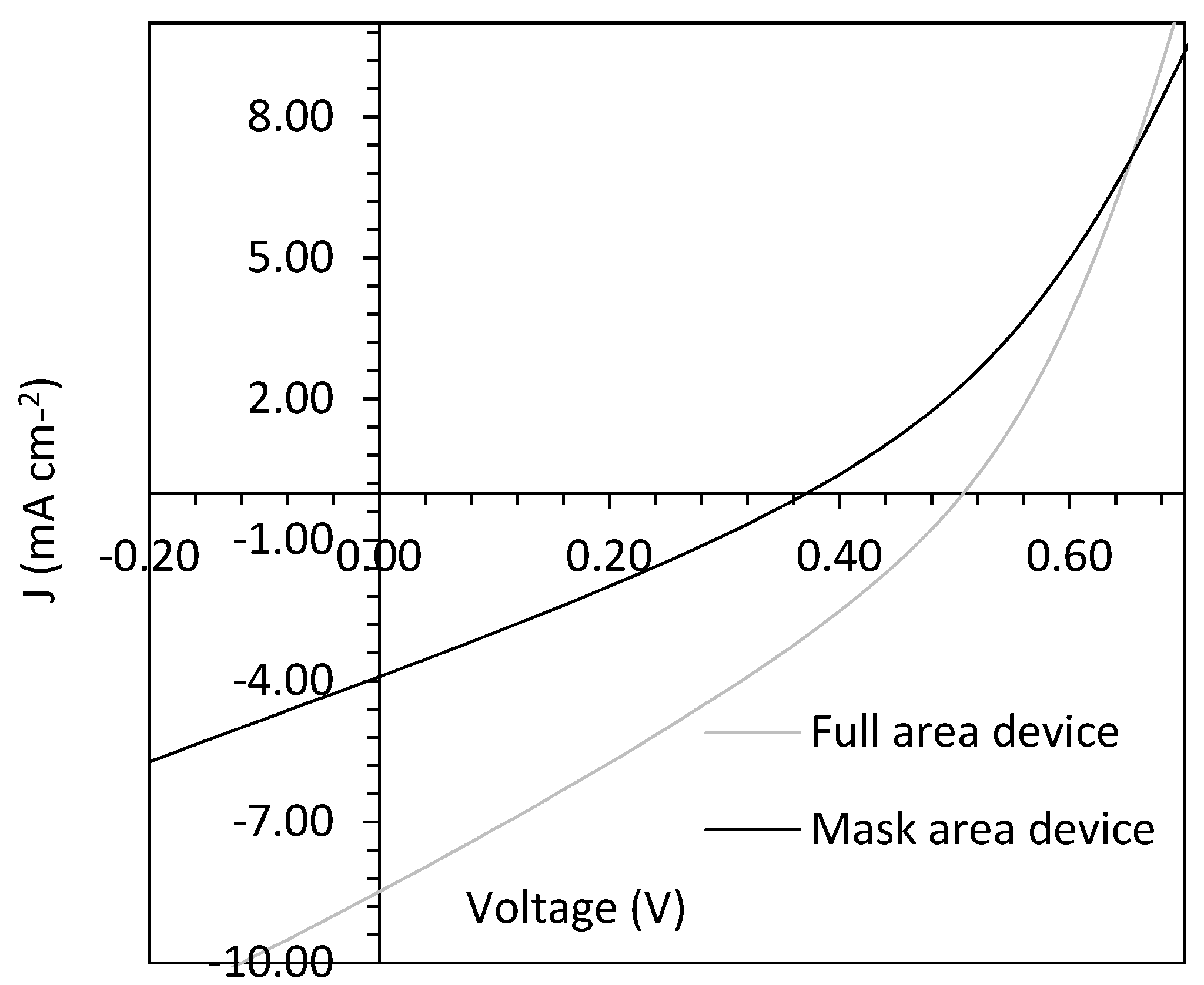
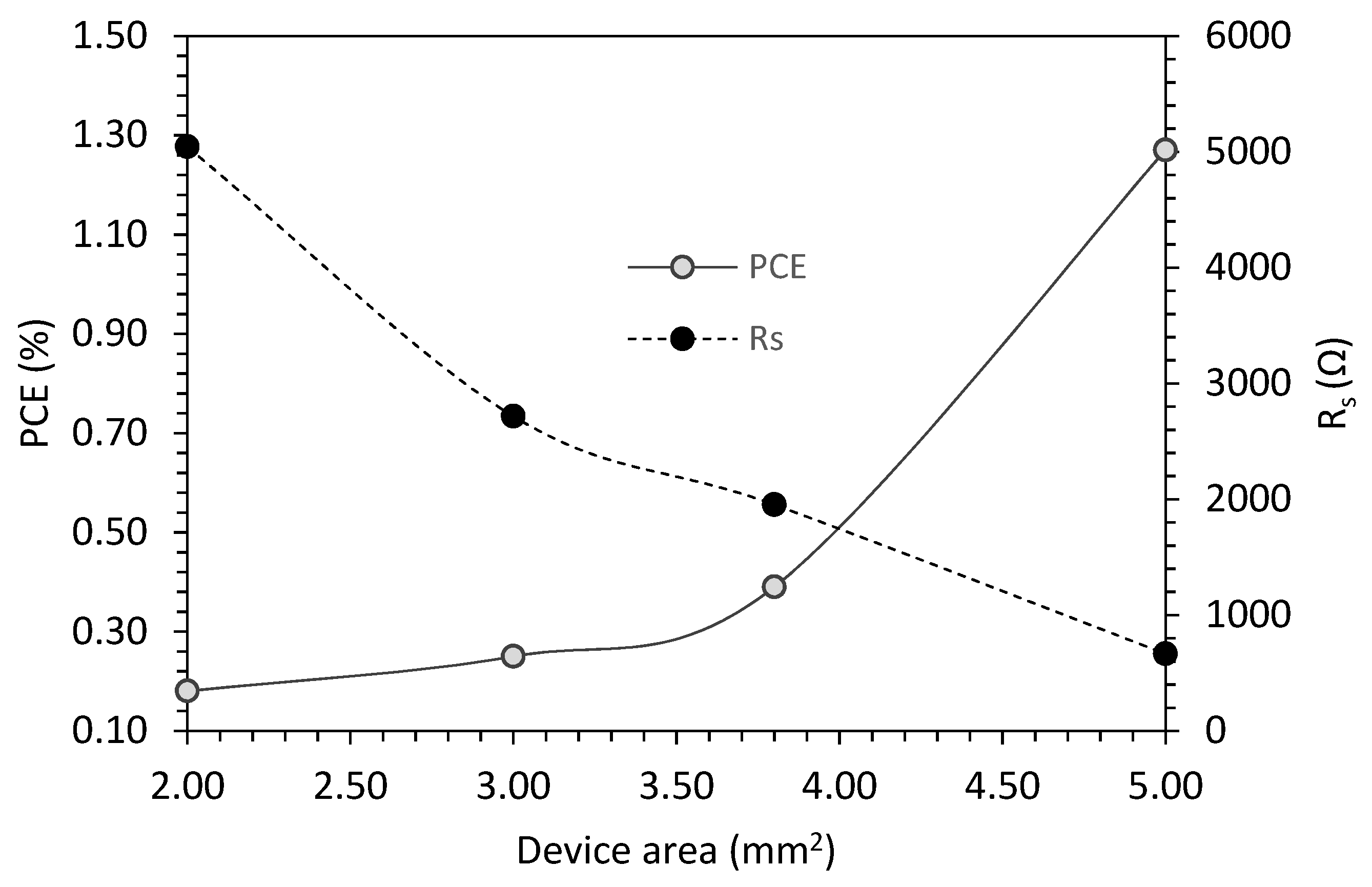
| Device Type | PCE (%) | Voc (V) | Jsc (mA/cm2) | Fill Factor | Cell Area (mm2) |
|---|---|---|---|---|---|
| OPV/G | 0.18 | 0.27 | 2.58 | 0.25 | 2 |
| OPV/G | 0.25 | 0.29 | 3.28 | 0.25 | 3 |
| OPV/G | 0.39 | 0.37 | 3.91 | 0.27 | 3.8 |
| OPV/G | 1.27 | 0.5 | 8.48 | 0.29 | 5 |
Publisher’s Note: MDPI stays neutral with regard to jurisdictional claims in published maps and institutional affiliations. |
© 2022 by the authors. Licensee MDPI, Basel, Switzerland. This article is an open access article distributed under the terms and conditions of the Creative Commons Attribution (CC BY) license (https://creativecommons.org/licenses/by/4.0/).
Share and Cite
Ali, A.Y.; Holmes, N.P.; Ameri, M.; Feron, K.; Thameel, M.N.; Barr, M.G.; Fahy, A.; Holdsworth, J.; Belcher, W.; Dastoor, P.; et al. Low-Temperature CVD-Grown Graphene Thin Films as Transparent Electrode for Organic Photovoltaics. Coatings 2022, 12, 681. https://doi.org/10.3390/coatings12050681
Ali AY, Holmes NP, Ameri M, Feron K, Thameel MN, Barr MG, Fahy A, Holdsworth J, Belcher W, Dastoor P, et al. Low-Temperature CVD-Grown Graphene Thin Films as Transparent Electrode for Organic Photovoltaics. Coatings. 2022; 12(5):681. https://doi.org/10.3390/coatings12050681
Chicago/Turabian StyleAli, Alaa Y., Natalie P. Holmes, Mohsen Ameri, Krishna Feron, Mahir N. Thameel, Matthew G. Barr, Adam Fahy, John Holdsworth, Warwick Belcher, Paul Dastoor, and et al. 2022. "Low-Temperature CVD-Grown Graphene Thin Films as Transparent Electrode for Organic Photovoltaics" Coatings 12, no. 5: 681. https://doi.org/10.3390/coatings12050681
APA StyleAli, A. Y., Holmes, N. P., Ameri, M., Feron, K., Thameel, M. N., Barr, M. G., Fahy, A., Holdsworth, J., Belcher, W., Dastoor, P., & Zhou, X. (2022). Low-Temperature CVD-Grown Graphene Thin Films as Transparent Electrode for Organic Photovoltaics. Coatings, 12(5), 681. https://doi.org/10.3390/coatings12050681