Article

ZnO Piezoelectric Films for Acoustoelectronic and Microenergetic Applications

1
Kotelnikov Institute of Radio Engineering and Electronics of RAS, 125009 Moscow, Russia
2
Acoustoelectronic and Piezokeramic ELPA Corporation, 125009 Moscow, Russia
*
Authors to whom correspondence should be addressed.
Coatings 2022, 12(5), 709; https://doi.org/10.3390/coatings12050709
Submission received: 20 April 2022 / Revised: 18 May 2022 / Accepted: 20 May 2022 / Published: 23 May 2022

Abstract

:
Zinc oxide is one of the most popular materials for acoustoelectronic sensors and vibro-piezo-transducers used in nano-piezo-generators. In the present paper, thick piezoelectric ZnO films are fabricated on both sides of various substrates using magnetron sputtering technique. It is shown that the main problem for double film deposition is the difference in thermal expansion coefficients of the ZnO films and the substrate materials. The problem is solved by decreasing the plate temperature up to 140 °C, reducing the growing rate up to 0.8 ± 0.05 μm/h, and diminishing the oxygen content in Ar mixture up to 40%. Using the modified sputtering conditions, the ZnO films with thickness up to 15 μm, grain size 0.3 μm, and piezoelectric module as large as 7.5 × 10⁻¹² C/N are fabricated on both faces of quartz and lithium niobate plates as well as on flexible polyimide flexible film known as Kapton. The films are characterized by chemical composition, crystallographic orientation, piezoelectric effect, and acoustic wave generation. They are applied for vibro-piezo-transducer based on flexible ZnO/Kapton/Al/ZnO/Al structure. When the structure is mechanical excited, the variable electric voltage of about 35 mV is generated. The value of the voltage is sufficient for an unstable energy source used in autonomic micro-energetic energy-store systems.

1. Introduction

Thanks to unique electric, optic, semiconductor, and piezoelectric properties, zinc oxide (ZnO)-based structures are very attractive for various electronic devices. As ZnO has a wide-band energetic zone (Eg ≈ 3.94 eV at T = 0 К and (3.37 ± 0.01) eV at room temperature), it possesses n-type conductivity and large energy of exciton coupling (60 mV).
Thin ZnO films are used in such fields as transistors, gas sensors, photo-voltaic devices, emission displays, nano-electro-mechanical systems, etc. [1,2,3]. For acoustoelectronic gas sensors, the film should have both good piezoelectric properties and strong adsorption facilities. The nature of sorption on the ZnO film surface (physical, chemical) and growth of the film defects (lattice, dislocations) may be monitored for changing conditions of the film growing, e.g., temperature, rate, and gaseous atmosphere.
One of the most promising acoustoelectronic sensors could be based on layered structures composed of a piezoelectric plate of one material and piezoelectric films of other materials (the same or different) deposited on one or two faces of the plates [4,5,6,7]. These structures allow monitoring sensitivity of the sensors by varying materials, film thickness, plate thickness, wavelength, propagation direction, and order of the acoustic mode. However, the multi-layered structures demand special conditions for depositing the layers in order to account for individual physical properties of each material of the structures, e.g., ZnO film from one hand and quartz, lithium niobate, and other plates from the other hand.
Thin ZnO films may be fabricated using different methods such as sol-gel, chemical vapor deposition (CVD), magnetron sputtering, molecular-beam epitaxial, laser ablation, etc. [3,8,9,10,11,12,13].
Piezoelectric properties of ZnO crystal are frequently exploited in different practical applications. It is known that the ceramic materials have macroscopic piezoelectric responses in cases when the crystal structure has no axis of inverse symmetry, but dipoles are aligned along one direction [14]. For ZnO, such direction is [0001] or C6 axis. C-oriented ZnO films may be growing as different nano-structures [15,16] and used in various sensors [1,13,16,17,18,19] and energy applications [20], including nano-generators [21,22].
The use of ZnO films in nanogenerators makes it possible to integrate them into microenergetic systems. The term “micropower” was proposed by Seth Dunn of the World Ecology Institute (Worldwatch Institute, Washington, DC, USA), who included solar panels, wind turbines, hydrogen cells, and gas microturbines in this category, i.e., low power generators [23]. However, when taking into account the technical and economic aspects of modern energy, the term “microenergy” must be interpreted more broadly, considering the problems of generating electricity using systems with energy storage based on heterogeneous sources, including unstable sources. Devices continuously converting various types of energy (mechanical, chemical, biological, solar, radio frequency, acoustic, thermal) into electricity can be used to create micro-energy systems with energy storage. Excess energy of technological and natural processes can be used in them. These micro-energy systems can be used to power off-grid mobile electronic gadgets, stationary power systems, and devices that require pulsed power applications to operate.
In energy storage systems, the pumped storage method is usually used. To implement this method, it is necessary to use special electronic devices that can work with low-energy sources and convert low voltage of the unstable sources into a standard operating voltage used in microelectronics.
Piezoelectric ZnO films on a flexible basis are used to effectively convert bending, vibrational, and acoustic vibrations into an electrical signal [24]. Previously, it was proposed to use polyimide films (Kapton) as a flexible base for the deposition of ZnO films [25]. It was shown that such ZnO films may have piezoelectric properties close to those of a single crystal.
The goal of the present paper is the investigation of the possibility of the production of complex multilayer structures containing materials with different thermal expansion coefficients using magnetron sputtering. Similar structures based on ZnO thin films can be used to develop various acoustic chemical sensors [4] and flexible vibro-piezo transducers for micropower devices [24].

2. Materials and Methods

Piezoelectric ZnO films with a C6 axis orientation perpendicular to a substrate surface were fabricated using a dc magnetron system (VSE-PVD-DESK-PRO, Novosibirsk, Russia). The oil-free vacuum system ensures high purity of deposited coatings. The specially developed design of the vacuum chamber additionally allows ion cleaning of the substrate surface before deposition. The system of smooth regulation of the average output power of the magnetron from 0.1 to 3 kW allows minimizing of the diameter of the non-sputtered central part of the magnetron target, controlling the process of coating deposition and, together with the automatic system for rocking the substrate in the region of the spray cone, makes it possible to ensure the uniformity of the thickness of the resulting coatings. To ensure the constancy of the gas composition of the working plasma, the working gas is supplied directly through the magnetron.
A combination of Ar (80%) and O2 (20%) is employed as a gas mixture at 0.07 Pa. During the sputtering, the temperature of the substrate is maintained at 250 °C. Discharge power was equal to 160 W. The growing rate, crystallite dimension, and maximal thickness of the film were equal to 1.25 ± 0.05 μm/h, 0.3 μm, and 15 μm, respectively.
A 5” diameter x 0.250” thickness disc of ZnO (99.9% purity), (Kurt J. Lesker Company Ltd., Jefferson Hills, PA, USA) was used as a sputtering target. As substrate for ZnO film sputtering a <111>-Si wafer with a thickness of 380 μm and diameter of 6” (Microchemical, Ulm, Germany), ITO glass (15–20 Ohm/sq) with a geometric size and thickness of 10 × 10 mm2, and 1.1 mm, respectively, (Biotain Crystal, Longyan, Fujian, China), and sapphire wafer with a thickness of 600 μm and diameter of 4”(Pam-Xiamen Co., Xiamen, China) were used.
A piezoelectric 128°Y-LiNbO3 and ST-SiO2 plates of 500 μm thick and 3” diameter (SPP, Fomos Materials, Moscow, Russia) were used during the modified sputtering regime as substrates for ZnO films.
As a flexible substrate, a polyimide film Kapton with a thickness of 50 μm (DuPont, Midland, MI, USA) was used.
The as-sputtered ZnO films were analyzed towards morphology, chemical composition, crystallographic orientation, and piezoelectric effect.
A field emission scanning electron microscope JSM-6390 (JEOL Ltd., Tokyo, Japan) was used for morphological analysis of the ZnO film obtained. The grain size distribution was determined by analyzing SEM images. In the case of isometric particles, the diameter is a characteristic of their size. For a sample with non-isometric crystals, the surface area was measured within the contour of the particle image. The measured surface area of the particle contour S ± ∆S was recalculated into an equivalent diameter using the formula d = (4 S/π)1/2. Sizes from 2000 to 3000 particles were determined using standard Image-Pro software. The sensitivity of the resulting distribution to the features of the disperse composition of the measured particles is greater, the greater their quantity.
The morphology, structural testing, and molecular composition of the ZnO films deposited on various substrates were studied by means Confocal Micro Raman Spectroscopy System HEDA250 (NOST Co., Ltd., Seoul, Korea). The focal length of the collimating lens (spectrometer base) is 250 mm. This allows measurements ranging from 50 cm−1 to 4500 cm−1 with a spectral resolution of 1.5 cm−1 for a laser with a wavelength of 532 nm. All regimes for controlling the laser power, correcting astigmatic aberration, and removing the luminescent component of the spectrum are set by means of a computer.
The composition of the films was determined using Shimadzu XRD-6000 diffractometers (Shimadzu, Columbia, MD, USA) with CuKα radiation within the range of 2θ = 10–70°. The experimental X-ray diffraction patterns were compared with the PDF-2 database.
Piezoelectric properties of the ZnO films are evaluated from the measurements of the normal piezoelectric module d33 along surface normal using experimental setup shown in Figure 1.
The probe in Figure 1 is working as follows. An electric pulse from a pulse generator (50–100 V, 0.1 μs) is supplied to a ceramic electromechanical transducer generated longitudinal bulk acoustic wave in the probe. The wave propagates from the top to the bottom of the probe and approaches the piezoelectric film, operating as an output electro-mechanical transducer. The signal from the film is amplified by video-amplifier and recorded by oscilloscope. Then, the film is substituted by a thin piezoelectric plate with known d33 that is placed on the same substrate without any film. By comparing the signals form the film under study and the plate, the film value of d33 is determined.
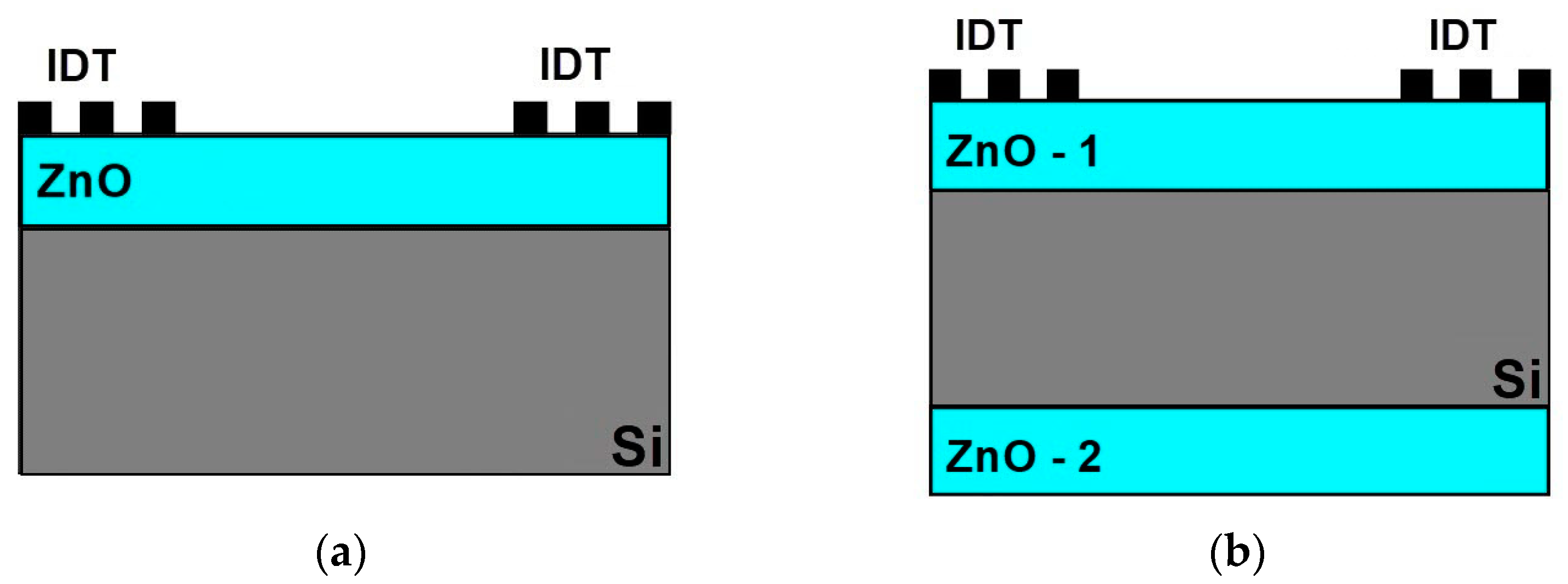
The efficiency of acoustic wave generation by ZnO films obtained was analyzed in the following way. The interdigital transducers (IDTs) are formed on one ZnO surface (Figure 2a). Each transducer is comprised of 20 finger electrodes followed with period λ = 20 or 200 μm patterned from 100-nm-thick V and 1000-nm-thick Al. Transducers with λ = 20 μm and λ = 200 μm are used for surface acoustic waves and acoustic plate wave mode generation, respectively.
IDTs were fabricated without using any photomasks, by means of a SmartPrint (Microlight 3D company, La Tronche, France) lithograph. The transducers are exposed on photo-resist deposited on ZnO film with a thickness of more than 8 μm during the drawing. The transparency of ZnO film and UV reflection from the substrate surface has been taken into account. The relevant draw in photo-resist was accomplished through a «lift-off» process. Finally, the metallic electrode of IDTs was sputtered using dc magnetron system (VSE-PVD-DESK-PRO, Novosibirk, Russia).
The measurements of the insertion loss S12(f) are carried out using KEYSIGHT 5061B network analyzer (Keysight, Santa Rosa, CA, USA) operating in amplitude-frequency format.
The next step in studying layered structure was the research and development of two-film prototypes, where two ZnO films with different thicknesses were deposited on opposite faces of a silicon plate (Figure 2b). Here, input and output IDTs located on one of the surfaces were fabricated using «lift-off» lithography. IDTs electrodes consisted of Al/V 0.3 μm thick. The specific resistance of the electrodes is about 0.14–0.15 Ω/sq.

3. Results

3.1. ZnO Films Characterization Results

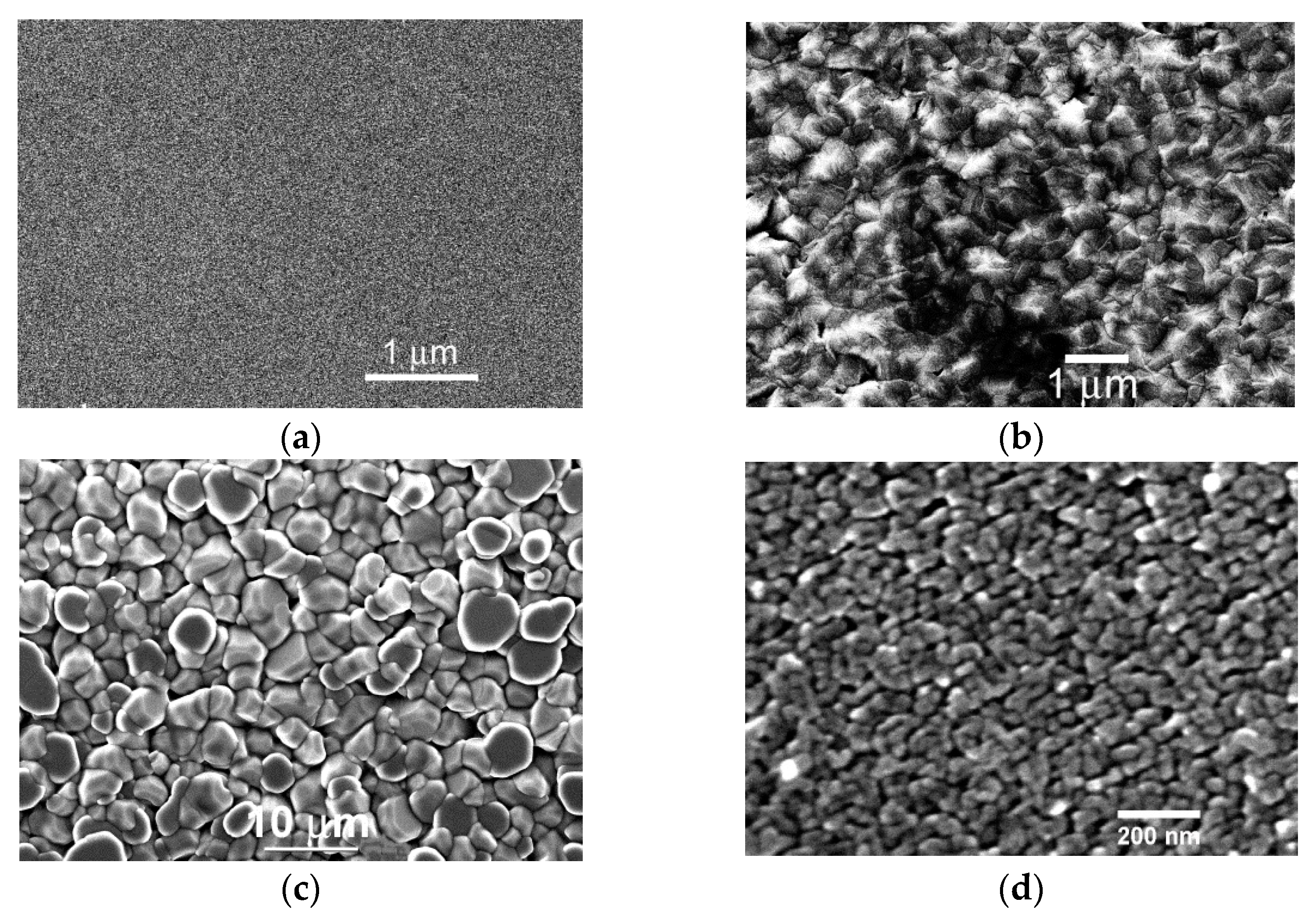
Figure 3 shows electron microscope imagines of ZnO films deposited on different substrates: (a) silicon; (b) conductive layer ITO on glass substrate; (c) sapphire; (d) Kapton (polyimide). It is seen that the microstructure of the films depends on the substrate.
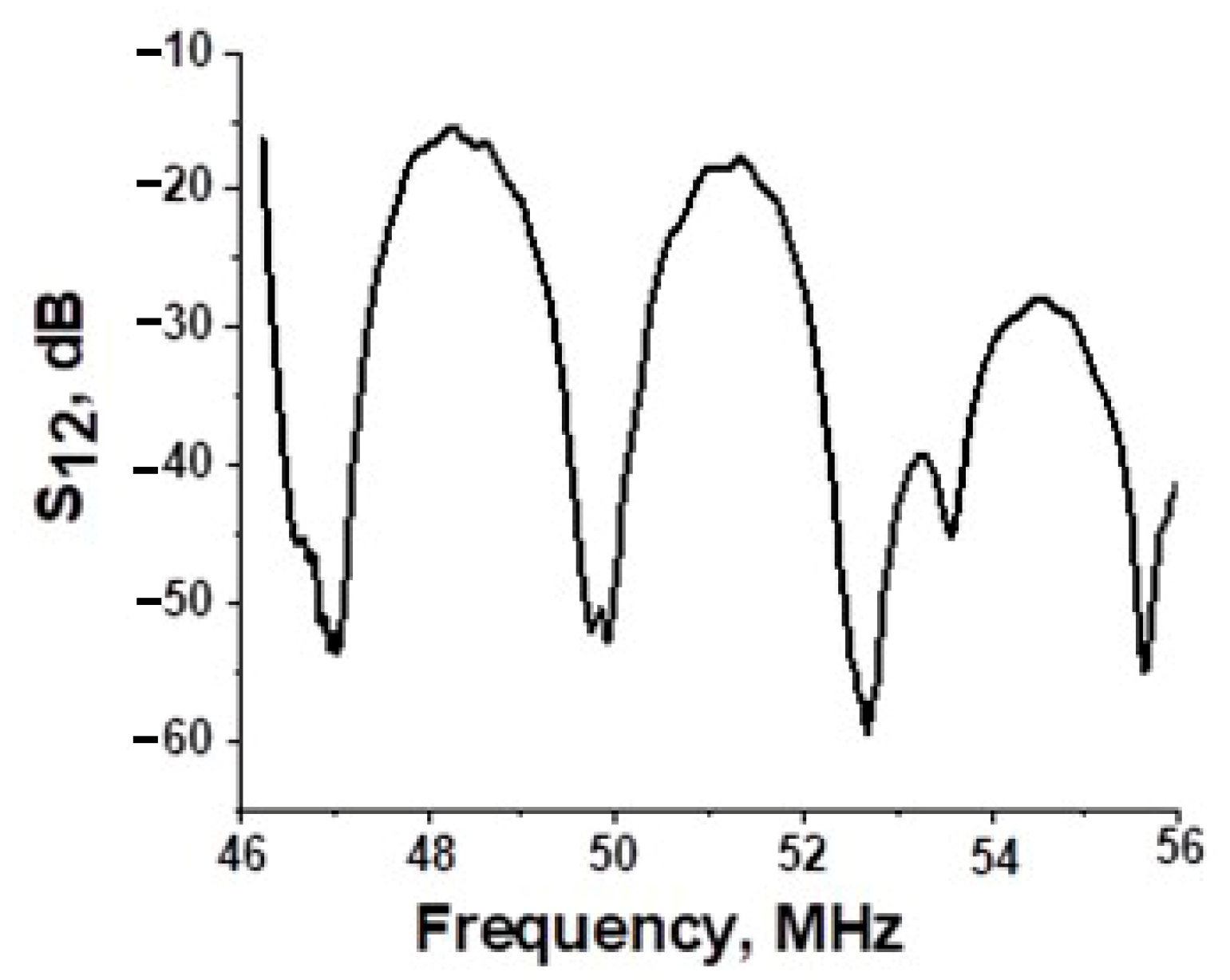
Figure 4 shows insertion loss of the ZnO-based acoustic delay line. The value of the loss is as low as 18–30 dB, indicating good electromechanical properties of the ZnO films. Three minima measured at different frequencies f are due to three acoustic plate modes, propagating in the structure with different phase velocities v (f = v/λ, where λ is period of IDT equal to the wavelength). Different amplitudes of the minima are due to various coupling constants of the modes. The wave velocities, frequencies, coupling constants, and mode amplitudes may be varied purposely by the changing the thickness of the ZnO-1 film, ZnO-2 films, and Si plate.
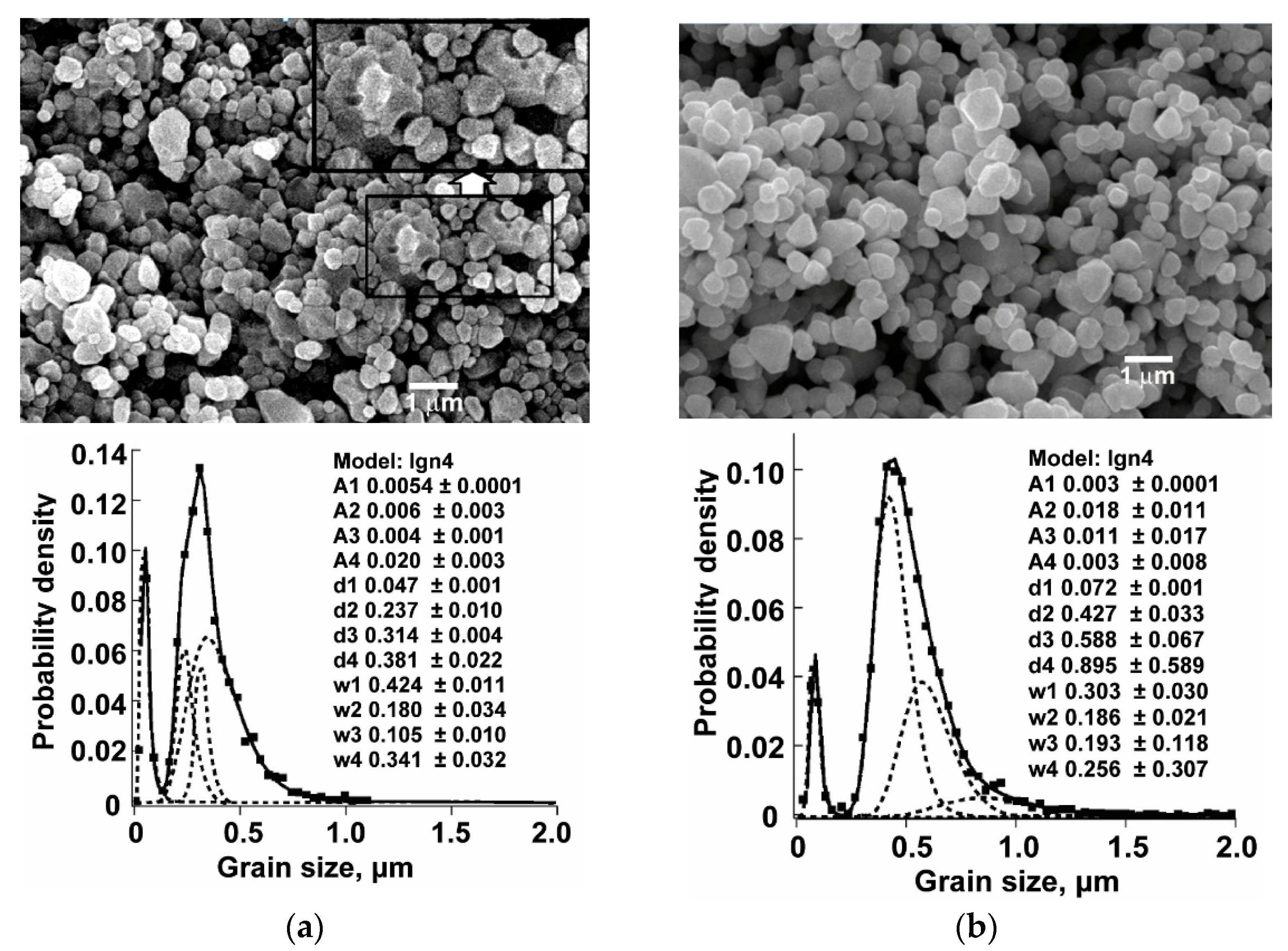
For micro-energetic devices based on vibro-piezo-transducers, the piezoelectric ZnO films are deposited on both faces of conductive flexible substrates. Figure 5 shows grain size distribution for ZnO film on aluminum (Al) and cuprum (Cu) layers measured by SEM. The size of the grains was determined using the Image-Pro standard program based on statistics from 2000 particles.
Distribution of the crystallites over the size on Figure 5a contains both a finely dispersed component and three components with overlapping size intervals. Similar dependences are observed for the sample in Figure 5b. The SEM images of the samples show that most crystallites have the same round shape of the particles. The crystallites of the sample in Figure 5b have smooth regular facets and a larger size, which is reflected in the total average size (D) of crystallites of 0.500 ± 0.005 µm.
The total average size and calculation error D ± ΔD were determined by averaging the sizes of all crystallites. Approximation of a distribution of the experimental points by size was performed using the log-normal function.
From the size distribution of the averaged crystallites size (d) the dispersed composition and two main parameters Ai and wi were determined for each component. The first is proportional to the number of crystallites of the component distribution and the second one is proportional to the distribution width, which depends on the homogeneity of the conditions for the formation of crystallites. The ratio Ai/ΔAi makes it possible to determine the proportion of component crystals in the total number of powder crystallites.
Figure 6 presents the Raman spectra of the ZnO films deposited on Al and Cu substrates, respectively. It is seen that the film grown on Al demonstrates narrower main pick and, thereby, smaller grain size as compared with those for Cu.

3.2. Modification of Piezoelectric ZnO Film Deposition

Recently, piezoelectric ZnO films deposited on silicon substrates may be as thick as 25 μm [26]. However, for plates of quarts and lithium niobate, it turned out to be impossible. The film thickness generates the main problem for the multilayered structures because of difference in thermal expansion coefficients of the film and the plate materials. Indeed, for ZnO, SiO2, and LiNbO3 materials, relevant coefficients are 5.5 × 10⁻⁶/°С, 13 × 10−6/°С, and 16 × 10−6/°С, respectively [27,28].
At the beginning, silicon substrate deposition of ZnO films was accomplished in a three-electron cathode DC system using ZnO target, Ar (80%) + O2(20%) gas mixture, and 0.07 Pa pressure. The substrate temperature and the growing rate of the film were 250 C and 1.2–1.3 μm/h, respectively. The ZnO films had good texture and piezoelectric properties close to those of a single crystal, but being fabricated on quartz and lithium niobate substrates at traditional conditions, the films destroy the substrates as shown in Figure 7a,b.
Mechanical destruction of the substrates is mainly attributed to tension deformation arising after the sputtering condition, when ambient air is introduced into the chamber or when the chamber is opened. Neither annealing the samples in Ar + O2 gas mixture, nor the annealing in inert Ar gas after sputtering, or processing the film in inert Ar atmosphere before opening the chamber solved the problem.
We assumed that the problem originated from intrinsic mechanical stresses that arose in the multi-layered structure due to different expansion coefficients of the structure components at too high temperatures. Therefore, to solve the problem we decided, first, to reduce the plate temperature up to 140 °C during the growing process and, second, to decrease bombardment of ZnO film by slowing the growing rate up to 0.8 ± 0.05 μm/h and by diminishing the oxygen content in the Ar mixture up to 40%.
The modified sputtering conditions are used for ZnO film deposition on polished faces of a piezoelectric 128°Y-LiNbO3 plate of 500 μm thick, piezoelectric ST-SiO2 plate of 500 μm thick, and nonpiezoelectric <111>-Si wafer of 380 μm thick. The latter was used for control. At modified conditions the plates of all materials are not destroyed (Figure 7c).
The structure of the ZnO films is studied by X-ray diffraction and rocking curves (Figure 8). The measured data confirm a high level of the film cleanness (stekhiometry) and weak disorientation of the crystallites (<±2°) towards the С6 axis for all plate materials.
The normal piezoelectric module d33 along surface normal was measured by means of the experimental setup (Figure 1). The typical response of the piezoelectric probe is presented in Figure 9 (horizontal scale is 1 μs/div, vertical scale is 10 mV/div). The response consists of the electro-magnetic leakage (the 1st signal at the beginning), the first acoustic pulse delayed with respect to the leakage on the time that is necessary for acoustic wave propagation from input ceramic transducer to the top of the probe, and few acoustic signals multi-reflected within the structure. The amplitude of the first acoustic pulse was proportional to the piezoelectric module d33 of the test piezoelectric film, while its “polarity” depends on orientation of the C6 axis; on Figure 9 the positive acoustic signal is for the C6 axis directed out of the film.
The signal for the film is compared with signal from the thin (50 μm) Y-cut litium niobate plate whose d33 is known (20.6 × 10⁻¹² C/N). For this, the plate is placed instead of the film on the same nopiezoelectric substrate and tested by the same probe. As diameter of the probe top is 1 mm, while grain size of the film is 0.3 μm, the d33 value measured by the probe is averaged over 30–40 ZnO crystallites. By moving the table in two mutually perpendicular directions, the d33 module is measured in different points on the film surface allowing an estimate of the film homogeneity.
The maximal value of d33 module measured for ZnO films fabricated at modified conditions is 9 × 10⁻¹² C/N or 85% of the same module for ideal single crystal ZnO.
The vibro-piezo-transducer was made as follows. A thin aluminum layer of 100 nm thick was deposited on one side of the Kapton film of 50 μm thick. Then, the ZnO film was sputtered on both sides of the Al/Kapton structure using a modified technique. Then, the other thin aluminum layer of 100 nm thick was deposited over the ZnO film grown on one side. A photo of as-fabricated vibro-piezo-transducer and its schematic view are shown in Figure 10a,b. Here, first ZnO film is used as an electric source, while the second one avoids twisting the Kapton plate. The d33 value of ZnO film on the plate was 7.5 × 10⁻¹² C/N. Two metal electrodes, visible on the left (Figure 10a), were in contact with the previously deposited aluminum layers. Then the resulting transducer was connected to an oscilloscope. Bending vibrations of the ZnO/Kapton/Al/ZnO/Al structure were mechanically excited. The variable electric voltage provided by bending vibrations of the ZnO/Kapton/Al/ZnO/Al structure was measured as 35 mV. The value of the voltage is sufficient for an unstable sources of energy in autonomic store-energy systems [29].

4. Discussion

The reduction of substrate temperature directly and through less effective bombardment of ZnO film due to smaller growing rate allows a decrease in mechanical stress in the film and fabricate textured layers on the substrates with rather different temperature expansion coefficients (quartz, lithium niobate, flexible Kapton substrates).
The reduction of oxygen content in the Ar mixture makes ZnO film less dense and, thereby, less variable with temperature; however, for friable ZnO films, larger acoustic attenuation is more inherent because of weak inter-atomic interaction at the crystallite-cristallite boundaries. Large acoustic attenuation in the film enlarges total propagation loss, but taking into account the small part of acoustic energy concentrated in the films, the total increase in insertion loss is not so much.
Figure 5 shows that ZnO film grown on Al substrate has a narrower Raman peak as compared with that one for its Cu counterpart. Therefore, the films on aluminum have smaller dimensions of ZnO crystallites. This result is supported by the data of Figure 4.
For effective acoustoelectronic devices, the texture of ZnO film up to 15 μm thick is deposited on both faces of quartz and lithium niobate plates. Varying the thickness of the films on the top and bottom faces of the plates allows monitoring acoustic wave properties purposely.
For vibro-piezo-transducers based on Kapton thick film, the textured ZnO thin films are deposited on both faces of the Kapton. This geometry of the transducers provides electric power generation when the structure is subjected to mechanical forces. RF voltage measured at output metal contacts of the structure is as large as 35 mV.

5. Conclusions

The modified sputtering method allowing fabrication of piezoelectric ZnO films on both surfaces of the substrates with very different thermal expansion coefficients is developed. ZnO films with normal piezoelectric module d33 equal to 7.5 × 10⁻¹² C/N are fabricated on quartz and lithium niobate plates using this method. The thickness of the films is as large as 15 μm.
Using the same technology, the ZnO films are also deposited on a flexible Kapton film 50 μm thick. The Al/ZnO/Al/Kapton/ZnO layered structure is applied for vibro-piezo-transducer operating as an unstable energy source. In this application, mechanical energy of the bending vibrations is converted into electric voltage used in an energy storage system and a special electronic DC-DC converter [29]. The variable electric voltage provided by the bending vibrations of the structure is 35 mV, making the transducer useful for autonomic systems of storage energy.

Author Contributions

Conceptualization, V.K. and V.A.; methodology, V.O.; software, I.K.; validation, E.G., V.K. and V.A.; investigation, E.G., V.K. and V.A.; resources, I.K.; writing—original draft preparation, V.K., V.A. and I.K.; writing—review and editing, V.K., V.A. and I.K.; visualization, E.G. All authors have read and agreed to the published version of the manuscript.

Funding

This research was funded by the Ministry of Science and Higher Education of Russia, government task of Kotelnikov IRE of RAS No FFWZ-2022-0002. The equipment of USU #352529 “Cryointegral” was used to carry out the research; USU is supported by a grant from the Ministry of Science and Higher Education of the Russian Federation, agreement No. 075-15-2021-667.

Data Availability Statement

Not applicable.

Conflicts of Interest

The authors declare no conflict of interest. The funders had no role in the design of the study; in the collection, analyses, or interpretation of data; in the writing of the manuscript, or in the decision to publish the results.

References

  1. Vyas, S. A short review on properties and applications of zinc oxide based thin films and devices: ZnO as a promising material for applications in electronics, optoelectronics, biomedical and sensors. Johns. Matthey Technol. Rev. 2020, 64, 202–218. [Google Scholar] [CrossRef]
  2. Borysiewicz, M.A. ZnO as a functional material, a review. Crystals 2019, 9, 505. [Google Scholar] [CrossRef] [Green Version]
  3. Wu, Y.; Ma, Y.; Zheng, H.; Ramakrishna, S. Piezoelectric materials for flexible and wearable electronics: A review. Mater. Des. 2021, 211, 110164. [Google Scholar] [CrossRef]
  4. Anisimkin, V.I.; Voronova, N.V. Acoustic properties of the film/plate layered structure. IEEE Trans. Ultrason. Ferroelectr. Freq. Control. 2011, 58, 578–584. [Google Scholar] [CrossRef]
  5. Kuznetsova, I.E.; Anisimkin, V.I.; Kolesov, V.V.; Kashin, V.V.; Osipenko, V.A.; Gubin, S.P.; Tkachev, S.V.; Verona, E.; Sun, S.; Kuznetsova, A.S. Sezawa wave acoustic humidity sensor based on graphene oxide sensitive film with enhanced sensitivity. Sens. Actuators B Chem. 2018, 272, 236–242. [Google Scholar] [CrossRef]
  6. Li, Z.; Meng, X.; Wang, B.; Zhang, C. A three-dimensional finite element analysis model of SAW torque sensor with multilayer structure. Sensors 2022, 22, 2600. [Google Scholar] [CrossRef]
  7. Xu, H.; Fu, S.; Su, R.; Shen, J.; Zeng, F.; Song, C.; Pan, F. Enhanced coupling coefficient in dual-mode ZnO/SiC surface acoustic wave devices with partially etched piezoelectric layer. Appl. Sci. 2021, 11, 6383. [Google Scholar] [CrossRef]
  8. Li, L.; Miao, L.; Zhang, Z.; Pu, X.; Feng, Q.; Yanagisawa, K.; Fan, Y.; Fan, M.; Wen, P.; Hu, D. Recent progress in piezoelectric thin film fabrication: Via the solvothermal process. J. Mater. Chem. A 2019, 7, 16046–16067. [Google Scholar] [CrossRef]
  9. Lee, J.B.; Kim, H.J.; Kim, S.G.; Hwang, C.S.; Hong, S.H.; Shin, Y.H.; Lee, N.H. Deposition of ZnO thin films by magnetron sputtering for a film bulk acoustic resonator. Thin Solid Film. 2003, 435, 179–185. [Google Scholar] [CrossRef]
  10. Kim, T.H.; Park, J.J.; Nam, S.H.; Park, H.S.; Cheong, N.R.; Song, J.K.; Park, S.M. Fabrication of Mg-doped ZnO thin films by laser ablation of Zn:Mg target. Appl. Surf. Sci. 2009, 255, 5264–5266. [Google Scholar] [CrossRef]
  11. Tsay, C.-Y.; Fan, K.-S.; Chen, S.-H.; Tsai, C.-H. Preparation and characterization of ZnO transparent semiconductor thin films by sol-gel method. J. Alloys Compd. 2010, 495, 126–130. [Google Scholar] [CrossRef]
  12. Fragalà, M.E.; Malandrino, G.; Giangregorio, M.M.; Losurdo, M.; Bruno, G.; Lettieri, S.; Amato, L.S.; Maddalena, P. Structural, optical, and electrical characterization of ZnO and Al-doped ZnO thin films deposited by MOCVD. Chem. Vap. Depos. 2009, 15, 327–333. [Google Scholar] [CrossRef]
  13. Nam, G.; Leem, J.-Y. Fast-response photoconductive ultraviolet light detectors fabricated using high-quality ZnO films obtained by plasma-assisted molecular beam epitaxy. Ceram. Int. 2017, 43, 11981–11985. [Google Scholar] [CrossRef]
  14. Zinc Oxide Bulk, Thin Films and Nanostructures: Processing, Properties, and Applications; Jagadish, C.; Pearton, S.J. (Eds.) Scopus, Elsevier Science: Amsterdam, The Netherlands, 2006. [Google Scholar]
  15. Wang, Z.L. Nanostructures of zinc oxide. Mater. Today 2004, 7, 26–33. [Google Scholar] [CrossRef]
  16. Bhati, V.S.; Hojamberdiev, M.; Kumar, M. Enhanced sensing performance of ZnO nanostructures-based gas sensors: A review. Energy Rep. 2020, 6, 46–62. [Google Scholar] [CrossRef]
  17. Chaudhary, S.; Umar, A.; Bhasin, K.K.; Baskoutas, S. Chemical sensing applications of ZnO nanomaterials. Materials 2018, 11, 287. [Google Scholar] [CrossRef] [Green Version]
  18. Elhosni, M.; Elmazria, O.; Petit-Watelot, S.; Bouvot, L.; Zhgoon, S.; Talbi, A.; Hehn, M.; Aissa, K.A.; Hage-Ali, S.; Lacour, D.; et al. Magnetic field SAW sensors based on magnetostrictive-piezoelectric layered structures: FEM modeling and experimental validation. Sens. Actuators A-Phys. 2016, 240, 41–49. [Google Scholar] [CrossRef] [Green Version]
  19. Shetti, N.P.; Bukkitgar, S.D.; Reddy, K.R.; Reddy, C.V.; Aminabhavi, T.M. ZnO-based nanostructured electrodes for electrochemical sensors and biosensors in biomedical applications. Biosens. Bioelectron. 2019, 141, 111417. [Google Scholar] [CrossRef]
  20. Theerthagiri, J.; Salla, S.; Senthil, R.A.; Nithyadharseny, P.; Madankumar, A.; Arunachalam, P.; Maiyalagan, T.; Kim, H.-S. A review on ZnO nanostructured materials: Energy, environmental and biological applications. Nanotechnology 2019, 30, 392001. [Google Scholar] [CrossRef]
  21. Savarimuthu, K.; Sankararajan, R.; Govindaraj, R.; Narendhiran, S. A comparative study on a flexible ZnO-based nano-generator using Schottky and p-n junction contact for energy harvesting applications. Nanoscale 2018, 10, 16022–16029. [Google Scholar] [CrossRef]
  22. Singh, H.H.; Khare, N. Flexible ZnO-PVDF/PTFE based piezo-tribo hybrid nanogenerator. Nano Energy 2018, 51, 216–222. [Google Scholar] [CrossRef]
  23. Dunn, S. Micropower: The next electrical era. Worldwatch Pap. 2000, 151, X-94. [Google Scholar]
  24. Yang, Z.; Zhou, S.; Zu, J.; Inman, D. High-performance piezoelectric energy harvesters and their applications. Joule 2018, 2, 642–697. [Google Scholar] [CrossRef] [Green Version]
  25. Joshi, S.; Nayak, M.M.; Rajanna, K. Evaluation of transverse piezoelectric coefficient of ZnO thin films deposited on different flexible substrates: A comparative study on the vibration sensing performance. ACS Appl. Mater. Interfaces 2014, 6, 7108–7116. [Google Scholar] [CrossRef]
  26. Zhao, X.; Huang, D.; Li, G.; He, Y.; Peng, W.; Li, G. High sensitivity X-ray detector based on a 25 µm-thick ZnO film. Sens. Actuators A Phys. 2022, 334, 113310. [Google Scholar] [CrossRef]
  27. Slobodnik, A.J. The temperature coefficients of acoustic surface wave velocity and delay on lithium niobate, lithium tantalate, quartz, and tellurium dioxide. Phys. Sci. Res. 1972, 1, 477. [Google Scholar]
  28. Tomar, M.; Gupta, V.; Sreenivas, K.; Mansingh, A. Temperature stability of ZnO thin film SAW device on fused quartz. IEEE Trans. Device Mater. Reliab. 2005, 5, 494–500. [Google Scholar] [CrossRef]
  29. Carlson, E.J.; Strunz, K.; Otis, B.P. A 20 mV input boost converter with efficient digital control for thermoelectric energy harvesting. IEEE J. Solid-State Circuits 2010, 45, 741–750. [Google Scholar] [CrossRef]
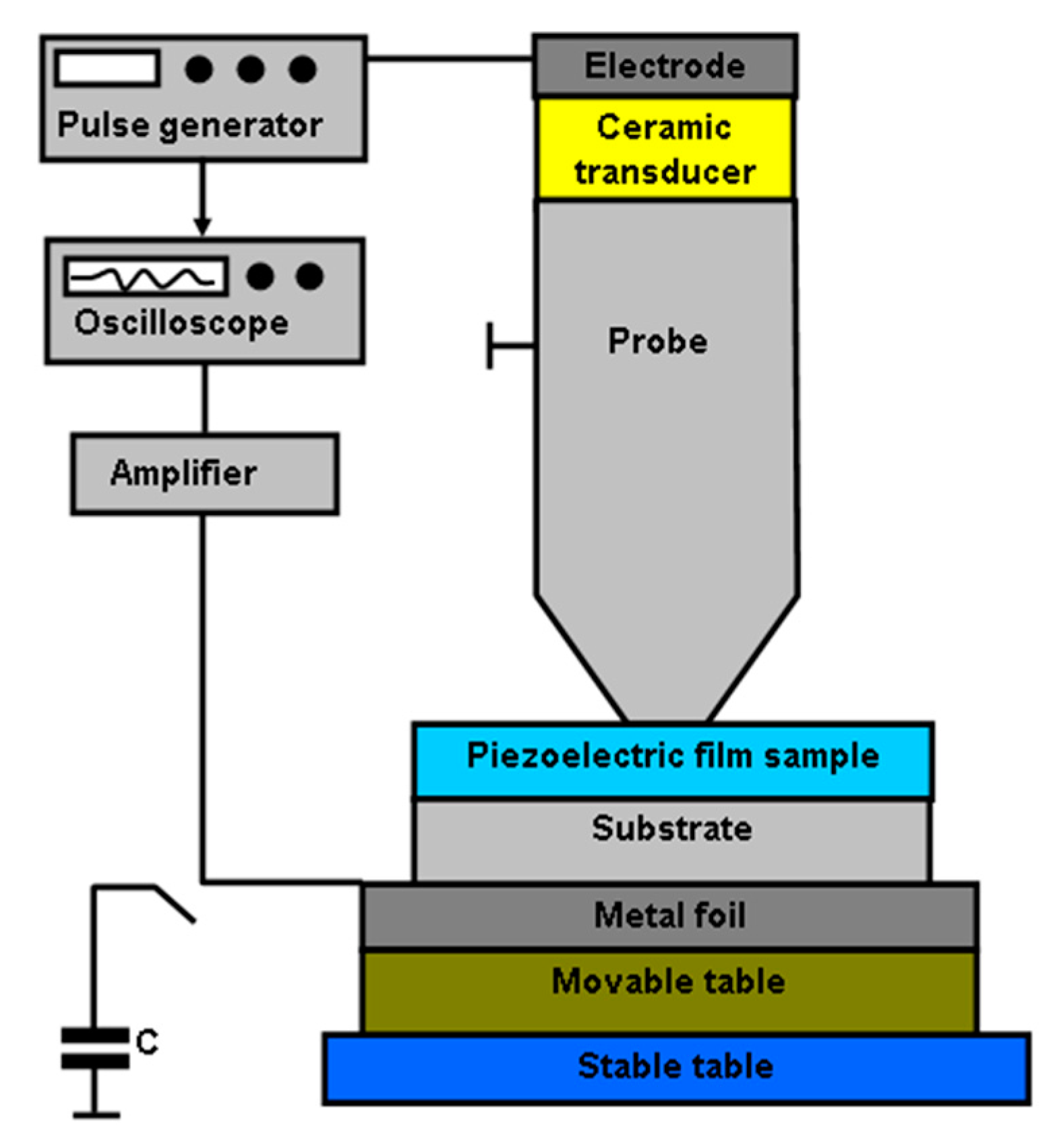
Figure 1. Acoustic probe used for piezoelectric component d33 measurement.
Coatings 12 00709 g001
Figure 2. General view of acoustic delay line based on: (a) single thin ZnO film deposited on Si substrate; (b) double-layered structure of two ZnO films deposited on Si plate.
Coatings 12 00709 g002
Figure 3. Electron microscope imagines of ZnO films deposited on the different substrates: (a) silicon; (b) ITO glass; (c) sapphire; (d) Kapton (polyimide).
Coatings 12 00709 g003
Figure 4. Insertion loss of the acoustic delay line based on ZnO-1/Si/ZnO-2 layered structure (Figure 2b) and acoustic plate modes propagating with different phase velocities. Si substrate thickness is 380 μm. ZnO film thicknesses are hZnO-1 = 8.8 μm, and hZnO-2 = 5.6 μm. IDT period λ = 146 μm.
Coatings 12 00709 g004
Figure 5. Grain size distribution of the ZnO film deposited on (a) Al with D = 0.320 ± 0.004 μm and (b) Cu with D = 0.5 ± 0.005 μm conductive sub-layers measured with SEM. D is the averaged value of the grains.
Coatings 12 00709 g005
Figure 6. Raman spectrum of the ZnO film deposited on: (a) Al layer; (b) Cu layer.
Coatings 12 00709 g006
Figure 7. Photos of the samples with ZnO film fabricated at traditional (a,b) and modified (c) sputtering conditions. (a) quartz plate, ZnO film thickness on one face of the plate is 8.2 μm, (b) lithium niobate plate, ZnO thickness on one face of the plate is 5.4 μm thick, (c) lithium niobate plate, ZnO film thickness on both faces of the plate is 5.4 μm thick.
Coatings 12 00709 g007
Figure 8. X-ray diffraction of the ZnO film fabricated at modified sputtering conditions on polished surface of <111>-Si plate.
Coatings 12 00709 g008
Figure 9. Typical piezoelectric response of the ZnO film measured with acoustic probe from Figure 2.
Coatings 12 00709 g009
Figure 10. The vibro-piezo-transducer (6 × 35 mm2) based on Al/ZnO/Al/Kapton/ZnO structure with two metallic electrodes (left). (a)—photo, (b)—schematic view.
Coatings 12 00709 g010
Publisher’s Note: MDPI stays neutral with regard to jurisdictional claims in published maps and institutional affiliations.