Abstract
In this study, we investigated the characteristics of the n-type Ni/SiC ohmic contact using the laser annealing process on thin wafers. The electrical behavior of the ohmic contacts was tested in 4H-SiC JBS diode devices. As a result, a wafer thickness of 100 μm in the 4H-SiC JBS diode achieved a forward voltage of 1.33 V at 20 A with a laser annealing process using Ni silicide. Using a laser annealing process on a wafer thickness of 100 μm, an on-resistance decrease of almost 22% was demonstrated. Based on our experimental results, we suggest an alternative laser annealing fabrication scheme to obtain low on-resistance SiC power devices with thin structures after SiC grinding.
1. Introduction
Compared to silicon (Si), silicon carbide (SiC) has a wide bandgap that provides a strong chemical bond among atoms and, therefore, a high electric breakdown field. SiC has an electric breakdown field roughly ten times that of silicon. Because of the strong atomic bond, SiC has greater lattice vibration and consequently, conducts energy more easily than Si. Therefore, SiC is a semiconductor material with good thermal conduction [1,2,3]. 4H-SiC is commonly used as a semiconductor material because it provides a better balance between electron mobility, low ON-resistance (RON), dielectric breakdown strength, saturation velocity, and other physical properties than other polytypes of SiC. However, the low fracture toughness, sensitive for cracking, high durability, and extreme hardness characteristics of SiC are predominant factors for its poor machinability. Efficient grinding of SiC requires optimizing wheel mesh and grind parameters to maximize removal rate while controlling surface integrity. Reportedly, the contribution of the substrate to RON in power devices with 350-μm 4H-SiC wafers amounts to 70% [2].
In this respect, the Junction Barrier Schottky (JBS) diode is forward-biased. Current flows go through the following path: anode metal → Schottky barrier metal → SiC epi. layer (N− drift) → SiC substrate (N+ layer). Therefore, the SiC substrate must be removed from the current path of the device to the largest extent possible without risking the manufacturing process by grinding. Such a contribution can reduce the RON by thinning the substrate by grinding [4].
Ohmic contact enhances reliability and reduces the on-resistance in SiC power devices. Ni is commonly used to form low-resistance n-type ohmic contact through the formation of nickel silicide with SiC. The rapid thermal annealing (RTA) process is generally used to form an ohmic contact, but the temperature required to form a Ni silicide layer with ohmic properties exceeds the melting temperature of commonly adopted front side metal. However, the use of the laser annealing process provides selective local annealing. It maximizes the effective annealing to the desired region to provide ohmic contact [5,6].
In this study, we investigated the characteristics of the n-type Ni/SiC ohmic contact using the laser annealing process on thin wafers. The behavior of JBS diodes with Ni-silicided backside contact reacting by laser-annealing was also studied for the final evaluation of the ohmic contact resistance properties.
2. Experimental
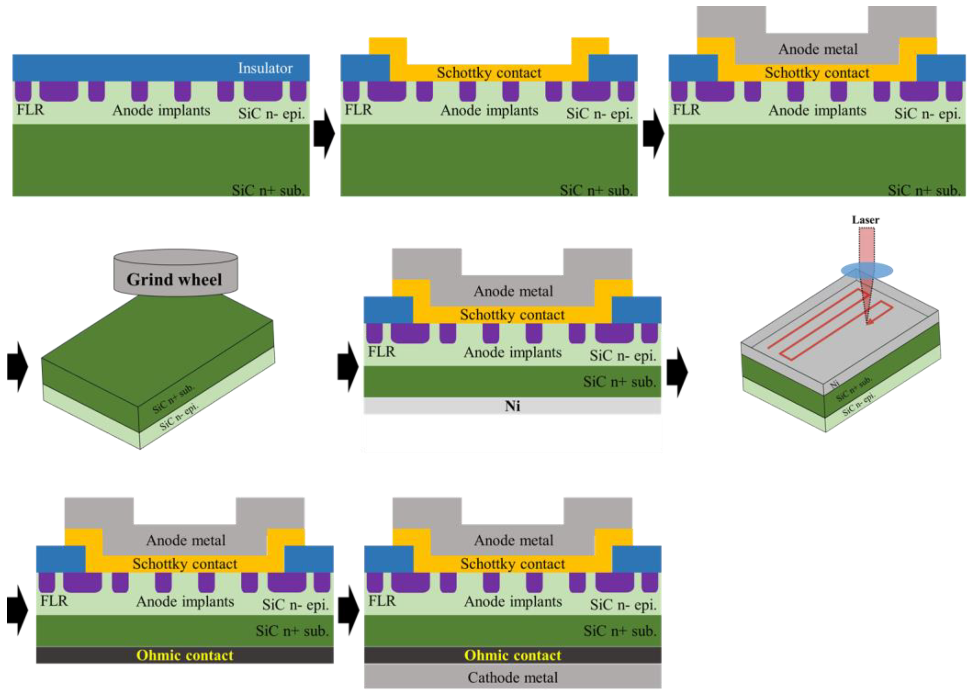
The JBS process flow is shown in Figure 1. JBS diodes were fabricated on n-type 4° off-axis epilayer 4H-SiC. The nitrogen concentration was 1.0 × 10¹⁶/cm3 and the epilayer thickness was 5.5 μm.

Figure 1.
Schematic flow chart of the fabrication of a JBS diode with grinding and laser annealing processes.
In the ion implant process, the Al ions were implanted through a mask of SiO2 to form a doped P-type (1.0 × 10¹⁸/cm3). Post-ion implantation annealing was conducted at 1700 °C in a nitrogen atmosphere during which the wafer was protected with a shielding layer on the front side.
Then, Schottky contact and anode metal were formed by sputtering and annealing, followed by back-side grinding and laser annealing processing.
Wafers were back-ground to 120, 170, and 330 μm using a back grinding machine with a 2000 mesh wheel and ground another 20 μm using a 7000 mesh fine wheel. Table 1. lists the wafer grinding thickness of the two wheels.

Table 1.
Thickness of the SiC wafer prior to and after grinding.
To form an ohmic contact, 100 nm-thick Ni was deposited on the SiC C-face (back-side) surfaces.
The silicide formation reaction between the Ni/SiC was induced by a laser annealing process of frequency 20 kHz, pulse width approx. 40 ns, beam size approx. φ100 um, and energy density 3.0 J/cm2 using a UV laser (wavelength, 355 nm).
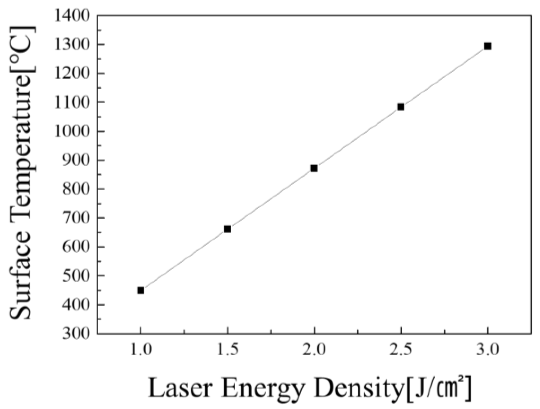
The laser beam overlapped 67% and 50% in the scan and step directions, respectively. The laser beam was 100 μm in diameter. The SiC to Ni interface temperatures of the ohmic contacts were extracted using a simulation tool with an equipment maker provided within the laser density of 3.0 J/cm2. The temperature of the SiC at a laser energy density of 3.0 J/cm2 was 1294 °C (Figure 2).

Figure 2.
The surface temperature simulation of energy density (provided by SHI).
Structural properties of the SiC C-face silicide layer were characterized by scanning electron microscopy (SEM). The JBS diodes were characterized by current-voltage (I–V) measurements using a Keysight B1505A source meter unit.
3. Results and Discussion
In our previous work, we showed that Ni became silicide after annealing at an RTA temperature of 1050 °C and that it could react with SiC. The ohmic contact properties on the n-type transfer length method (TLM) patterns at an RTA temperature of 1050 °C showed a contact resistance of about 10–5 Ω·cm2. Generally, the laser annealing process of the TLM pattern for silicide contact resistance measurements is not proper. When the laser beam strikes, the TLM pattern, ohmic metal, and SiC surface have a different absorption coefficient. The different areas cause problems, a rough and irregular surface morphology. Therefore, the laser annealing process was integrated with the fabrication of a 4H-SiC JBS diode, and the results were compared with the RTA approach at 1050 °C. Similar RTA JBS electrical properties were seen in the laser-annealed JBS diode at an energy density of 3.0 J/cm2 [7].
Figure 3 shows the structure of the SiC C-face, including the Ni silicide and cathode metal layer, using cross-sectional SEM imaging. The structure of the Ni silicide formed by laser annealing differed significantly from that of RTA silicide.
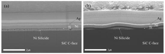
Figure 3.
(a) RTA silicide ohmic contact and (b) laser silicide ohmic contact cross-sectional SEM images for the SiC C-face of Ni thicknesses of 100 nm in the fabricated JBS diodes.
In the case of the RTA sample, the Ni silicide thickness showed a uniform trend in the SEM cross-section image. However, in the laser annealed sample, the cross-section was not uniform due to the presence of craters surrounded by curbs. Similar structures were reported in our previous study in samples irradiated at a high energy density 3.8 J/cm2.
To analyze the role of wafer thickness in laser annealing on ohmic contact, we focused on the behavior of different wafer thicknesses at an energy density of 3.0 J/cm2.
The forward characteristics of the as-deposited Ni layer and the laser-annealed JBS diode as a function of the I-V were measured using an I-V curve tracer.
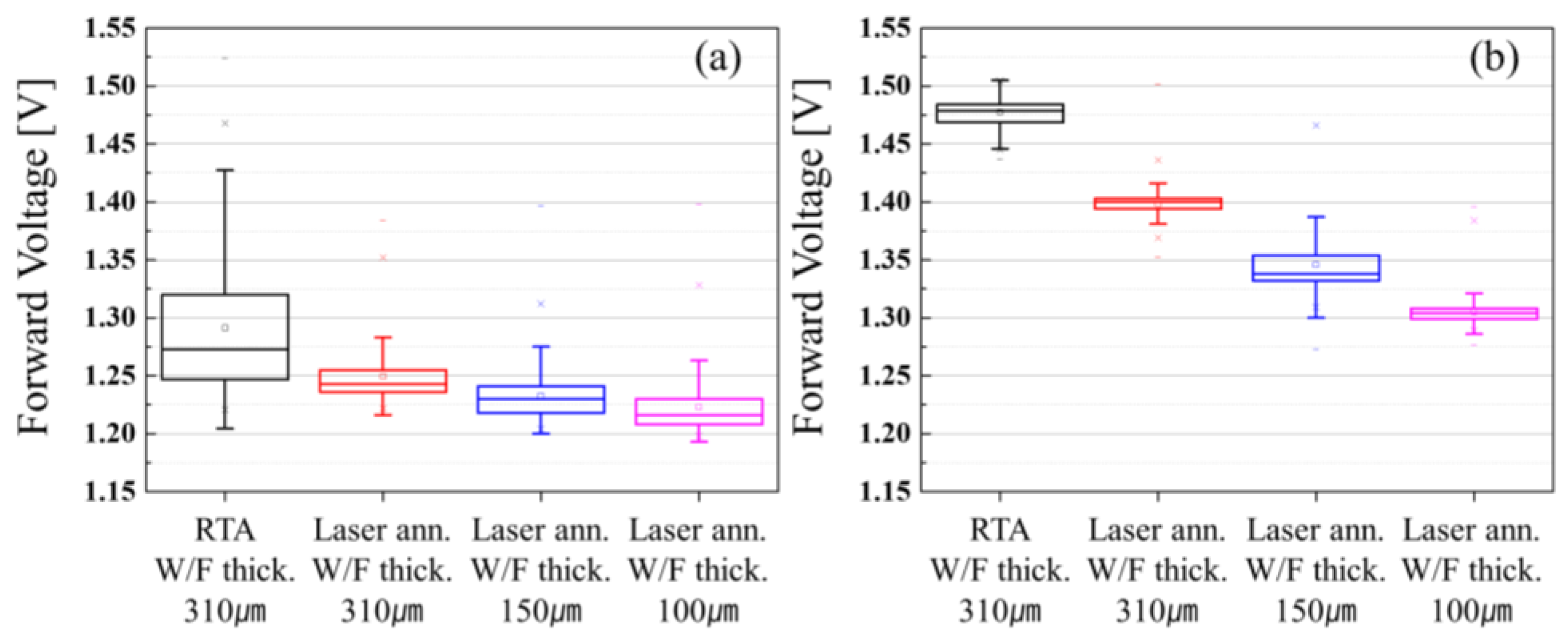
Figure 4 shows the forward voltage at a laser energy density of 3.0 J/cm2 at wafer thicknesses of 100, 150, and 310 μm compared to the RTA process at a wafer thickness of 310 μm using a 650 V SiC JBS diode. In Figure 4a, the laser-annealed JBS diode is compared to the RTA-processed JBS diode at a current of 10 A on the wafer, which confirmed that ohmic contacts were formed on the thin wafers by the laser annealing process. Additionally, the forward voltages of the JBS diode package (TO-220) were measured at 20 A, the forward current was extracted from the IV curves, and the results are shown in Figure 4b. The ohmic contact properties of the JBS diode fabricated by the RTA and laser processes with the same wafer thickness of 310 μm in the extracted TO-220 package at a forward current 20 A were a median of 1.47 and 1.40 V, respectively. The forward voltage of the laser-annealing JBS process decreased by almost 0.07 V at 20 A compared to the RTA JBS process. The results showed that laser annealing may have advantages such as better device performance over the RTA process for Ni-SiC silicidation formation. Additionally, the laser annealing process has the possibility of handling a range of <310 µm thick SiC wafers.

Figure 4.
The forward bias properties of fabricated JBS diodes at (a) a current of 10 A on wafer die chips and (b) a current of 20 A on TO-220 packages.
The forward voltage for JBS diodes with wafer thicknesses of 100 and 150 μm made via the laser annealing process at a current of 20 A was a median of 1.33 and 1.30 V, respectively. The on-resistance calculated by dividing the voltage by the current of a 100-μm-thick wafer (laser ann.) at a current level of 20 A was almost 22% lower than that of a 310-μm-thick wafer (RTA). The calculated on-resistance of wafer thickness 310 μm and 100 μm at current of 20 A was a median of 73 and 65 mΩ, respectively.
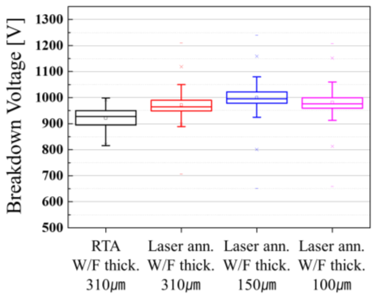
Figure 5 shows the breakdown voltage was similar to that of different types of JBS diodes. The breakdown voltage for wafer thicknesses of 100 to 310 μm was a median of 928 to 995 V.
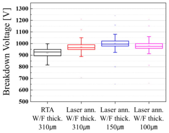
Figure 5.
The breakdown voltage properties of fabricated JBS diodes at a current of 250 μA in TO-220 packages.
The reverse bias of thin wafers with laser annealing was nearly same as that of RTA for JBS diodes, as shown in Figure 5. The results indicated that reverse bias during wafer thinning and the laser annealing process had no significant impact on JBS diodes.
Substrate resistivity was a contributor to the diode total on-resistance. The thickness of a thin substrate had a direct impact on the forward voltage when the diode was in the on-state. Therefore, it is best to reduce the wafer thickness to lower the forward voltage while considering mechanical stability. Thin wafer technology allows for the reduction of the wafer thickness to 100 μm. At a 100-μm wafer thickness, the reduced total on-resistance led to a 0.17 V reduction in the forward voltage for identical chip sizes.
Reduced chip thickness also leads to improved thermal resistance, which, in return, is beneficial for the power dissipation of the device. A thinner substrate layer offers a shorter thermal path for the heat generated inside the Schottky junction and drift layer of the JBS diode. The heat spread from the junction is enhanced, thus reducing the thermal resistance between the junction and the package lead frame or case.
4. Conclusions
In this paper, we reported the electrical characterization of Ni-SiC silicide ohmic contact in the RTA and laser annealing processes. The electrical behavior of the ohmic contacts was tested on 4H-SiC JBS diode devices. Thinning the JBS diode is expected to offer improved on-resistance and widen the possible applications of SiC power devices. Using a laser annealing process on a wafer thickness of 100 μm, an on-resistance decrease of almost 22 % was demonstrated. Improvement in the laser anneal silicide ohmic contact and SiC back-side grinding can lead to even further improvement in the impressive electrical characteristics achieved with SiC power devices. Based on our experimental results, we suggest an alternative laser annealing fabrication scheme to obtain low on-resistance SiC power devices with thin structures after SiC grinding.
Author Contributions
Conceptualization, K.K. (Kihyun Kim) and S.Y.; Data curation, K.K. (Kihyun Kim), Y.K., S.Y., E.J., and J.H.; Formal analysis, S.Y., C.Y., E.J., J.H., and K.K. (Kyunghwan Kim); Investigation, K.K. (Kihyun Kim), Y.K., S.Y., C.Y., and E.J.; Project administration, C.Y., E.J., and K.K. (Kyunghwan Kim); Writing—original draft, K.K. (Kihyun Kim); Writing—review & editing, K.K. (Kyunghwan Kim) All authors have read and agreed to the published version of the manuscript.
Funding
This work was supported by the Technology Innovation Program 20003935 funded by the Ministry of Trade, Industry, & Energy (MOTIE, Korea).
Institutional Review Board Statement
Not applicable.
Informed Consent Statement
Not applicable.
Data Availability Statement
Not applicable.
Conflicts of Interest
The authors declare no competing financial interest.
References
- Kimoto, T. Material science and device physics in SiC technology for high-voltage power devices. Jpn. J. Appl. Phys. 2015, 54, 040103. [Google Scholar] [CrossRef]
- Roccaforte, F.; Brezeanu, G.; Gammon, P.M.; Giannazzo, F.; Rascunà, S.; Saggio, M. Schottky contacts to silicon carbide: Physics, technology and applications. Adv. Silicon Carbide Electron. Technol. Met. Contacts Silicon Carbide Phys. Technol. Appl. 2018, 37, 9781945291852-3. [Google Scholar]
- Rascunà, S.; Badalà, P.; Tringali, C.; Bongiorno, C.; Smecca, E.; Alberti, A.; Di Franco, S.; Giannazzo, F.; Greco, G.; Roccaforte, F.; et al. Morphological and electrical properties of Nickel based Ohmic contacts formed by laser annealing process on n-type 4H-SiC. Mater. Sci. Semicond. Process. 2019, 97, 62–66. [Google Scholar] [CrossRef] [Green Version]
- Badalà, P.; Rascunà, S.; Cafra, B.; Bassi, A.; Smecca, E.; Zimbone, M.; Bongiorno, C.; Calabretta, C.; La Via, F.; Roccaforte, F.; et al. Ni/4h-sic interaction and silicide formation under excimer laser annealing for ohmic contact. Materialists 2020, 9, 100528. [Google Scholar] [CrossRef]
- Roccaforte, F.; La Via, F.; Raineri, V. Ohmic contacts to SiC. Int. J. High Speed Electron. Syst. 2005, 15, 781–820. [Google Scholar] [CrossRef]
- Rupp, R.; Kern, R.; Gerlach, R. Laser backside contact annealing of SiC power devices: A prerequisite for SiC thin wafer technology. In Proceedings of the 2013 25th International Symposium on Power Semiconductor Devices & IC’s (ISPSD), Kanazawa, Japan, 26–30 May 2013; pp. 51–54. [Google Scholar]
- Kihyun, K.; Yehwan, K.; Moonkoyng, N.; Seungbok, Y.; Sangik, C.; Inho, K.; Wook, B.; Eunsik, J.; Changheon, Y. Reduced Ohmic Contact Resistance and Improved 4H-SiC Junction Barrier Schottky Diodes Performance by Annealing on C-face Ohmic Regions in Ni/SiC Structures. In Proceedings of the KIEEME Annual Autumn Conference, Gyeongju, Korea, 11 May 2020; p. PA-39. [Google Scholar]

Publisher’s Note: MDPI stays neutral with regard to jurisdictional claims in published maps and institutional affiliations. |
© 2022 by the authors. Licensee MDPI, Basel, Switzerland. This article is an open access article distributed under the terms and conditions of the Creative Commons Attribution (CC BY) license (https://creativecommons.org/licenses/by/4.0/).