Article

Reactive Sputtered Ytterbium Silicate Environmental Barrier Coatings for Protection of Mo-Si-Based Alloys

German Aerospace Center (DLR), Institute of Materials Research, 51147 Cologne, Germany
*
Author to whom correspondence should be addressed.
Coatings 2022, 12(8), 1086; https://doi.org/10.3390/coatings12081086
Submission received: 30 June 2022 / Revised: 22 July 2022 / Accepted: 26 July 2022 / Published: 31 July 2022
(This article belongs to the Section Corrosion, Wear and Erosion)

Abstract

:
The implementation of a structural material into the hot section of a turbine engine requires the protection against oxidation and water vapour. Since Mo-Si-based alloys do not provide this protection on their own over a long period of exposure time, the necessity for protective coatings becomes inevitable. Rare earth silicates, especially Yb-silicates, are known for their great potential to protect silica against water vapour recession and also for their oxidation protective behaviour due to their low silica reactivity. Reactive pulsed DC co-sputtering was investigated and used to produce a two-layered coating of Yb2Si2O7 and Yb2SiO5. The layers were implemented into a four-layered environmental barrier coating system combined with a bond coat consisting of a graded Mo-Si interlayer and a thin Si top layer intended to form slow-growing silica. The EBCs were tested up to 100 h at 1200 °C and 800 °C isothermally in air on top of three different Mo-Si-based alloys and show promise for oxidation protection. The pesting phenomenon was completely suppressed.

1. Introduction

Ytterbium silicates are of high interest as environmental barrier coatings (EBC) for protection of SiC-SiC materials against water vapour corrosion [1,2,3,4,5]. The coatings are known for their low silica activities of 0.194 at 1415 °C for the Yb2Si2O7/Yb2SiO5 phase field and 0.00298 for the Yb2SiO5/Yb2O3 phase field, which provides a low rate of volatilisation up to 1400 °C [6]. The monosilicate Yb2SiO5 (YbMS) shows a lower recession rate compared to the disilicate Yb2Si2O7 (YbDS) [7]. Though, the protection of the underlying coatings and materials is given by preventing the penetration of water vapour. Since the silica formation is proportional to the vapour pressure of water (PH2O), the EBC should also provide a sufficient oxidation resistance [8,9]. Compared to other rare earth silicate candidates, Yb-silicates exhibit a high phase stability with no structural phase transition at high temperature with the stable phases β-Yb2Si2O7 and X2-Yb2SiO5 [10]. Two metastable phases are also known as α-Yb2Si2O7 and X1-Yb2SiO5 [11,12]. The coefficient of thermal expansion (CTE) of the YbMS is about 7.4 × 10⁻⁶ °C−1 and that of the YbDS is about 4 – 6 × 10⁻⁶ °C−1. Therefore, the Yb-silicates are promising as protection for Mo-Si-based alloys and SiC-based CMC’s [13].
In previous years, several deposition techniques were introduced to apply Yb-silicate EBC systems. Zhong et al. deposited a three-layered system of Si/Yb2Si2O7/Yb2SiO5 on a SiC-based substrates using the air plasma spraying technique (APS) for the first time. An excellent thermal shock resistance was proven by testing 50 cycles of 15 min hot (1350 °C) followed by water quenching (25 °C) [14]. Richards et al. also used APS to deposit a bi-layer Si/Yb2Si2O7. The coating system withstand a steam cycle (90% H2O/10% O2) using 60 min hot (1316 °C) and 10 min cold (110 °C) up to 2000 cycles [15]. In a study by Bakan et al., Yb2Si2O7 coatings were deposited by several thermal spray methods like APS, high velocity oxygen fuel spraying (HVOF), suspension plasma spraying (SPS), and very low-pressure plasma spraying (VLPPS). VLPPS was found to be the preferred method due to the formation of an almost fully crystalline, dense coating microstructure without vertical cracks [4]. In a different study, Bakan et al. used APS to introduced a two layered system of Si and mixed YbMS/YbDS layer. The coatings were tested until 200 h at 1200 °C under high velocity water vapour (100 m/s) [16]. In general, thermally sprayed Yb-silicate coatings suffer from a loss of silica during spraying and are therefore mostly not phase pure. Despite their low water vapour recession rate, Yb-silicates are also providing some oxidation protection since they lower the oxygen inward diffusion. Reactive magnetron sputtering was used by Leisner to deposit a two layered system of Si and YbDS. The YbDS coatings showed heavy pore agglomerations during furnace cycle testing in lab air until 1000 h at 1250 °C but still protected the SiC substrate efficiently against oxidation and against water vapour recession [17]. Garcia et al. used APS to produce a double layer Si plus a mixed YbDS/YbMS coating system to successfully test the oxidation resistance until 200 cycles at 1200 °C [12].
The reactive pulsed DC magnetron sputtering, which was investigated in this study, was also applied by Leisner et al. on Yttrium di- and monosilicate (YDS and YMS) EBC coatings [17,18]. A SiC substrate with a 10 µm thick underlying pure Si bond coat was coated with a 10 µm thick YDS and a 9 µm thick YMS layer. The coating system was tested until 1000 h thermocycle at 1250 °C in air and started to show pore formation, delamination and cracks at the YDS-YMS interface after 100 h.
In this study, an Yb-silicate EBC system consisting of an YbDS and YbMS layer was produced by reactive pulsed DC magnetron co-sputtering. Unlike in the studies mentioned above, the used substrate material was Mo-Si-based alloys. Mo-Si-based alloys, especially Mo-Si-Ti alloys, show great potential as structural materials for turbine engines [19,20]. Their CTEs range from 5 ×10⁻⁶ °C−1 to 6 ×10⁻⁶ °C−1 for Mo-9Si-8B to Mo-12.5Si-8.5B-27.5Ti-2Fe, and for Mo-21Si-34Ti-0.5B alloy, they range 7.2 × 10⁻⁶ °C−1 to 7.8 × 10⁻⁶ °C−1; these are in line with the Yb-silicates. Therefore, adhesion and stresses, caused by a mismatch in CTEs, should not be a problem [21,22]. In previous papers, the development of a silica forming oxidation protective coating was shown firstly by depositing a pure Si layer on the Mo-Si-based alloy which showed promising oxidation potential [23]. Secondly, a coating system consisting of a graded Mo-Si interlayer and a Si top layer was deposited on Mo-Si-based alloys. The graded interlayer could improve the adhesion of the coating system. The oxidation protection potential could be shown at 800 °C and 1200 °C until 300 h [22,24]. Since the silica that protected the underlying Mo-Si-based alloys against oxidation will suffer from steam enhanced oxidation and water vapour recession in a similar manner as on SiC-SiC, an EBC system preventing this degradation is necessary to be applied on top of the oxidation protection coatings.
In the current study special emphasis was put on the process parameters to ensure a stable and reproducible deposition of Yb-silicate layers with a maximal oxygen content and a high deposition rate. A cation ratio of c(Yb)/c(Si) = 2 for YbMS and for YbDS a cation ratio of c(Yb)/c(Si) = 1 was targeted. Furthermore, the crystallisation process and the development of the coating morphology was investigated. Afterwards, the Yb-silicates were applied on Mo-Si-based alloys with a Si-based bond coat to prove adhesion and oxidation resistance at 1200 °C.

2. Materials and Methods

The substrate material used for the development of the Yb-silicate coatings was commercially available corundum (Final Advanced Materials GmbH, Germany) with the dimensions 1 mm × 20 mm × 30 mm and a surface roughness of Ra = 0.6. The Mo-Si-based substrate material for the oxidation tests was manufactured in an arc melter (AM/0.5, Edmund Buehler GmbH, Germany) with a water-cooled copper crucible under Ar atmosphere at the Karlsruher Institute of Technology (KIT). Three different alloys were tested with the chemical composition of Mo-9Si-8B (at %), Mo-12.5Si-8.5B-27.5Ti-2Fe and Mo-21Si-34Ti-0.5B [22,24]. Their sample size of about 2 mm × 10 mm × 15 mm was achieved by wire cutting and surface preparation by a vibratory tumbler combined with grinding until 1200 grid.
The coating development took place in an industrial size coating facility (IMPAX, Systec SVS vacuum coatings, Karlstadt, Germany) with pulsed DC power supplies. Two rectangular metallic targets with the dimensions of 200 × 100 mm2 were used, one pure Yb target and one pure Si target (Sindlhauser Materials GmbH, Germany), with a distance of about 226 mm to the substrate holder. The deposition temperature was set at 150 °C by additional heating. Reactive co-sputtering was employed to generate the Yb-silicates by using oxygen carefully to simultaneously avoid significant target poisoning. The process was controlled by setting the target power; therefore, the curves of the currents were not displayed here. The pulse frequency was set to 40 kHz with a 6 µs reverse time in between. The pulsed DC supply suppresses arcs and can preferentially disperse oxides when local poisoning occurs, which is advantageous with respect to long coating processes. The Ar flow was set to 200 sccm.
The Yb-silicate coatings were X-ray amorphous after deposition. Thus, a crystallisation treatment was necessary and was carried out at 900 °C for one hour followed by one hour at 1200 °C in a box furnace under lab air conditions without interrupting the annealing. This crystallisation treatment was chosen due to the former studies on Mo-Si-based materials in order to compare the results after oxidation testing [23,24]. For the oxidation tests, the samples were further hold for 10 h to 100 h at 1200 °C and for 100 h at 800 °C right after the crystallisation treatment. The temperature of 800 °C was chosen due to the pesting phenomenon of Mo at intermediate temperatures [22].
Various analytical methods were used such as X-ray diffraction (XRD) (Bruker D8 Advance, Cu Kα radiation, EVA/Topas 4.2 software package, Bruker AXS, Karlsruhe, Germany), which revealed the phases and the phase evolution after the oxidation tests. In order to understand the crystallisation, high-temperature XRD (HT-XRD) was carried out with a heating furnace chamber (HTK 1200N, Anton Paar, Graz, Austria) within the Bruker D8 Advance. The measurement started at 30 °C and was heated until 900 °C with a heating rate of 60 °/min. After staying at 900 °C for one hour, the temperature was increased until 1200 °C with a heating rate of 10 °/min. A scanning electron microscope (SEM) (DSM Ultra 55, Carl Zeiss NTS, Wetzlar, Germany) was used to analyse the morphology with a voltage of 5 kV. Additionally, energy-dispersive X-ray spectroscopy (EDS) (Aztec, Oxford Instruments, Abingdon, UK) was executed at 15 kV to support the XRD results and reveal the local composition.

3. Results

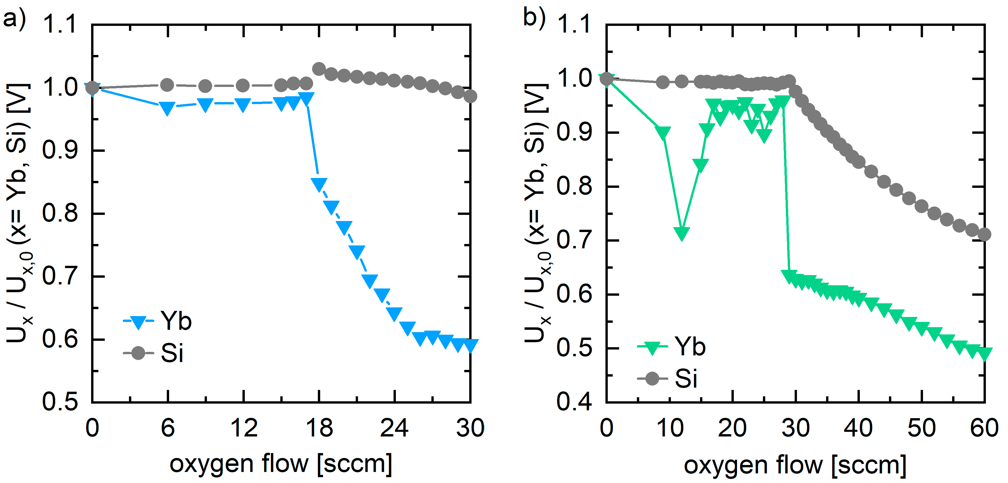
3.1. Reactive Pulsed DC Co-Sputtering

The great challenge of the reactive sputtering process is to prevent the target surface from poisoning. The process control, the process stability and also the properties of the deposited layers, especially the chemistry, are highly influenced by it [25]. During poisoning, parts of the metallic target surface form oxides with the reactive oxygen gas, which leads to a considerably reduced sputtering rate [17]. In order to find the right processing window for the deposition, the three modii of the target surface—namely metallic, transition of metallic and oxidic, and oxidic—need to be determined. In the case of co-sputtering without a reactive gas, the cation ratio of the deposited layer depends on the respective target power, the sputter yield of the elements as well as the atomic mass, which determines the distance dependence of the vapour cloud. If the atomic mass was left out and re-sputtering processes would be negligible, the cation ratio would depend proportionally on the ratio of the erosion rates of both targets. Unfortunately, this relationship applies to reactive sputtering only to a limited extent, since the oxygen flow and thus the nonlinear target poisoning are added as further influencing variables. The sputtering yields of the metals under argon at a 90° angle of incidence and an energy of 1 keV are given as 3.484 for Yb and 0.874 for Si in [26]. Based on preliminary experiments, the target power of Si should not exceed 1.2 kW in the used sputter facility to avoid target cracking and instabilities. To achieve the desired chemical ratios for the coatings, the Yb sputtering yield was reduced by over 50 % to match the Si. In Figure 1, the two discharging behaviours of Yb and Si are shown, which describe the chemical state of the target surface as a function of the oxygen flow, plotted only for the increasing gas flow part of the hysteresis. The curves were achieved by increasing stepwise the oxygen flow (3 sccm steps and 1 sccm steps) and holding every step for 2 min time while applying a constant target power through the whole process. The backward course is not of interest for the coating process, so it was left out. For the YbDS discharge curves (Figure 1a), the parameters 0.8 kW Yb target power and 1.2 kW Si target power were chosen. The YbMS discharge curves (Figure 1b) were implemented with the parameters 1.2 kW for Yb and 0.9 kW for Si.
From the discharging curves, the desired deposition windows for the coatings were derived. While the process was intended to produce oxygen-saturated coatings but still retain a high sputter rate, the parameters should lie within the transition zone starting at around 18 sccm up to 24 sccm oxygen flow for the YbDS composition given in blue according to Figure 1a. All points of the YbDS curve could be operated in transition mode quite stably. After 17 sccm oxygen, the first drop of 15% in voltage was observed. Simultaneously, the Si curve increases slightly before levelling again at the same voltage as started. The minimum of the Yb discharging voltage was reached at 250 V, which is about 58 % of the starting voltage by operating at 30 sccm oxygen. The Yb discharge curve displayed a rather unstable process between 9 sccm and 28 sccm in Figure 1b. The Yb target produced a lot of arcing and only ran stable after 28 sccm was achieved. The discharging curve was terminated at 60 sccm where no clear plateau could be found at 238 V. Between 28 sccm and 29 sccm, the Yb voltage fell about 33 % to about 300 V. At the same time, the Si voltage drops continuously almost parallel to the Yb voltages until 60 sccm of oxygen flow. Compared to the Yb discharging curve in Figure 1a, the Yb discharging curve in Figure 1b was offset by about 147 % for the first drop and by over 200 % for reaching the minimal voltage. The right operation point is thereby hard to determine; thus, different parameter combinations were evaluated. For YbDS, a ratio of c(Yb)/c(Si) = 1 and for YbMS c(Yb)/c(Si) = 2 or slightly higher was desirable, preventing SiO2 precipitates within the coatings while the oxygen content within the coating should be 50 at % or higher. By using a systematic variation of process parameters, in this case the power ratio Yb/Si and the oxygen flow, their influence on the chemical composition of the coatings was screened and is shown in Figure 2. The target power was varied for Yb between 0.7 and 1.6 kW, while the target power of Si varied between 0.95 kW and 1.5 kW. The oxygen flow was adjusted between 5 sccm and 29 sccm but was mostly set around 20 sccm to 23 sccm. The right cation ratio of YbMS and YbDS is highlighted, while the colour code indicates the oxygen content measured by EDS. The red circles around certain squares represent all depositions with an oxygen flow of 21 sccm. When the oxygen flow was kept constant at 21 sccm, the data seemed to follow the same trendline, which is represented by the red dotted line. Since all red circled squares lay within the desirable oxygen content range, the parameters for the final YbDS and YbMS coating could be extracted from the trendline. For the deposition of the YbDS, a target power supply ratio of about 0.8, and for the YbMS, a coefficient of about 1.3 was found.
In Figure 3, the final deposition process was represented with the corresponding as-coated microstructure. The YbDS layer was sputtered first for 175 min and was represented with a straight Si voltage line with minor arcing. The Yb voltage slowly increased from about 300 V to 450 V, where it suddenly dropped to about 100 V. At around 175 min, the process was changed into sputtering YbMS, which can be seen by the change in both target powers. The YbMS process showed arcing of the Si target combined with a rhythmic poisoning of the Yb target, which represented the fast decrease in voltage. Beforehand, the Yb target voltage increased shortly, while right after, the Si target voltage dropped before running constant again. Due to the longer deposition times in comparison to the initial screening experiments, the chosen process parameters were not stable but especially the Yb voltage fluctuated, indicating an ongoing change between transition and metallic mode or oxidic mode and back. The oxygen flow was increased slightly from 21 sccm at the YbDS to 22 sccm for the YbMS to keep the chamber pressure stable. The underlying microstructure shows clearly the impact of the Yb target voltage change within the YbMS coating.

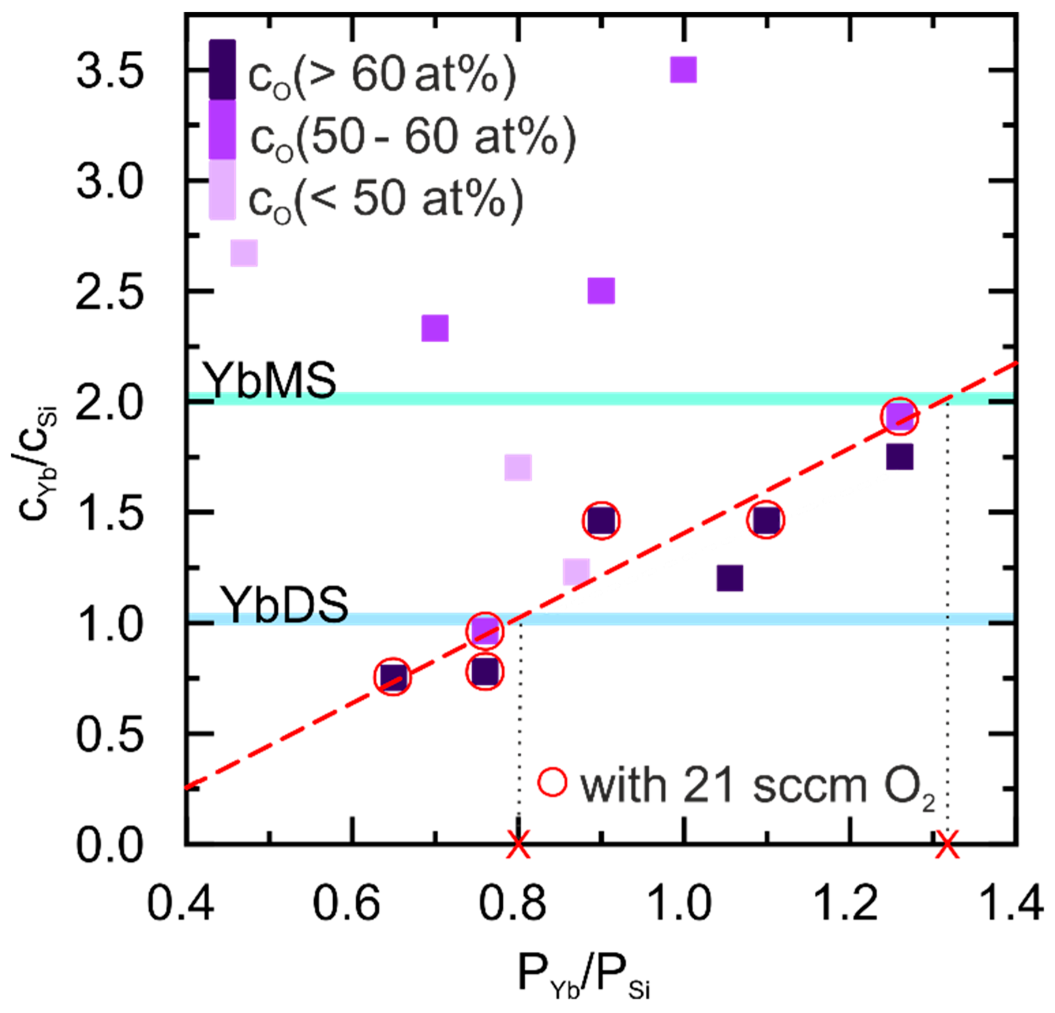
3.2. Analyses of Yb2SiO5 and Yb2Si2O7 Deposited Layers

The produced Yb-silicate coatings were X-ray amorphous, which required a post-crystallisation treatment. In order to understand the mechanisms of the crystallisation and the phase formation, HT-XRD was executed simulating the crystallisation treatment of the Yb-silicates deposited on an Al2O3 substrate. The parameters of the heat treatment were derived from the graded Mo-Si plus Si oxidation protection layers and were applied here as well for comparison. All samples except the ones measured in HT-XRD were annealed in a box furnace for 1 h at 900 °C followed by 1 h at 1200 °C, which was followed by cooling down to room temperature.
The XRD results are presented in Figure 4a. Since the samples were usually placed in an already pre-heated furnace, the fast heating rate was chosen to reach 900 °C as fast as possible. Figure 4b shows the scans as-coated, at 900 °C, at 1200 °C, and after crystallisation at room temperature (RT), 30 °C. Between a temperature range of 480 °C and 550 °C, SiO2 as cristobalite (PDF 03-0272) and Yb2O3 (PDF 43-1037) crystallised first. Both oxides transform between 1023 °C and 1035 °C into the β-Yb2Si2O7 phase (PDF 82-0734) and the X2-Yb2SiO5 phase (PDF 40-0386). Since YbMS is on top of the YbDS coating, YbMS could be measured more clearly with more intense peaks. In another measurement, not shown in this paper, the coating was deposited in the opposite sequence where YbDS consequently was measured with a higher intensity compared to the underlying YbMS. Since the coatings shown here had a slightly higher Yb content, Yb2O3 can be identified even after the silicates were formed, but some silica also remained in the coating after Yb-silicate formation as well.
The resulting microstructure of the Yb-silicate coatings on the inert substrate, Al2O3, are represented in Figure 5 using SEM and the EDS line scans. In Figure 3, the as-coated state showed a columnar but dense amorphous YbDS layer until the Yb target reached its highest voltage of about 450 V at around 160 min. At this point, the contrast became lighter, see Figure 5a, which indicates a high Yb content and a lower oxygen content, as shown in the EDS scan (Figure 5d). The amorphous YbDS layer in Figure 5a presented a slightly higher Yb concentration compared to silicon especially shortly before switching to YbMS. These findings were directly linked to the process data in Figure 3. During the deposition of the YbMS, high-voltage peaks of the Yb target are responsible for the layered structure. The Yb-rich microlayers are not as dense, which is why they are partly washed away during preparation. In the amorphous YbMS layer, recurring high Yb concentrations were measured accompanied by oxygen and silicon decreases (Figure 5d). After crystallisation, the YbDS layer formed a homogenous two-phase microstructure of YbDS and most likely YbMS (Figure 5b). In the YbMS layer, the thin, Yb-rich layer was again visible in a lighter greyscale due to a material contrast. Moreover, pore formation started especially within the Yb-rich regions of the YbMS layer. The cation ratio Yb to Si in the YbDS layer was about 1.5 and in the YbMS, it was 2.4 overall. The ratio depended highly on the location because of the two-phase microstructures of both layers (Figure 5e). After 10 h at 1200 °C, the YbDS coating remained a dense, two-phase microstructure with possibly YbMS precipitates (Figure 5c). The YbMS coating was still split into multilayers of YbMS of about 480 nm and Yb-rich thin layers of about 150 nm. The pore formation increased at the interface region between YbDS and YbMS as well as at the surface of the dual-layer coating. Furthermore, the pores seemed to increase in size in comparison to after crystallisation. The linescan in Figure 5f showed no differences compared to the crystallised coatings. The oxygen content was stable already after crystallisation at about 65 at %.

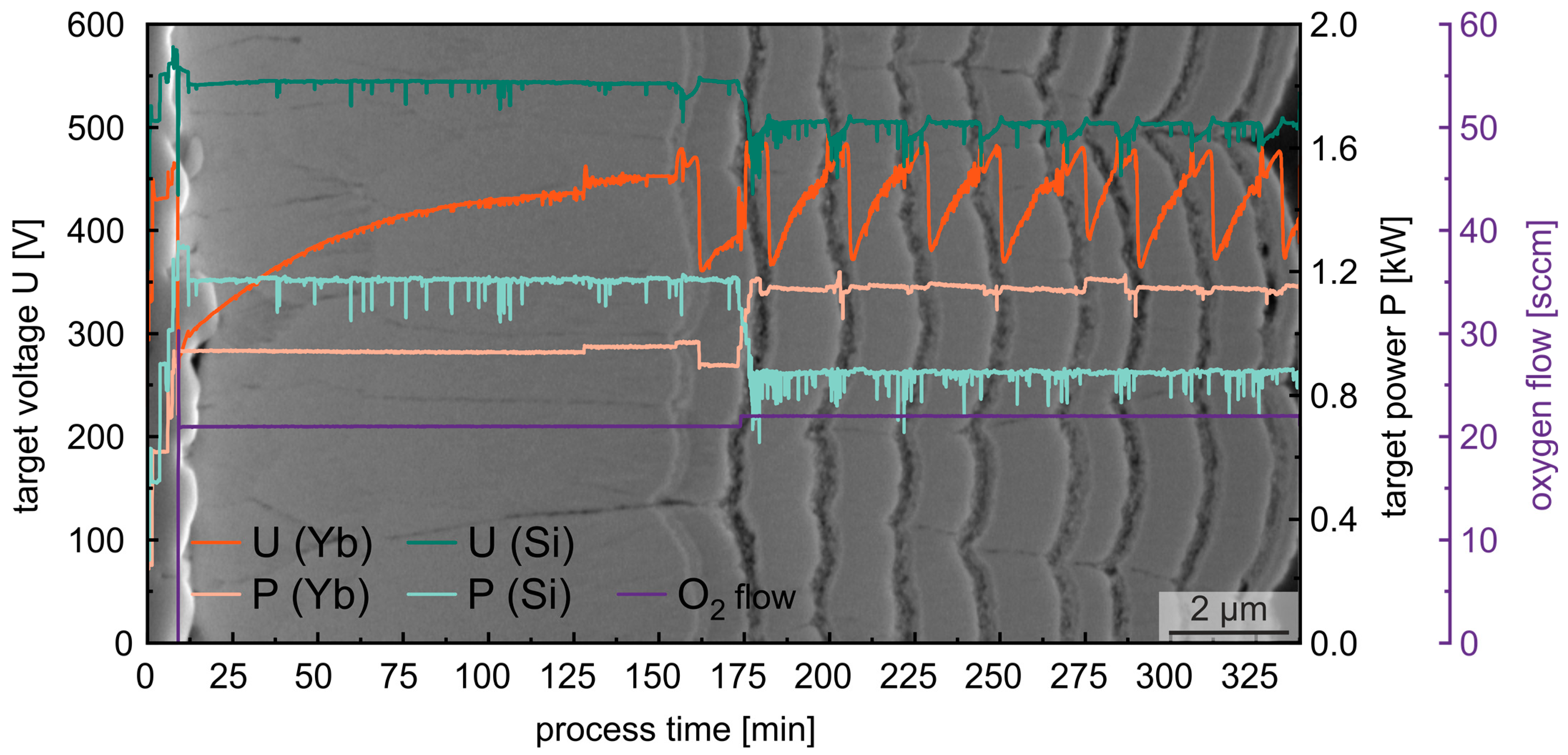
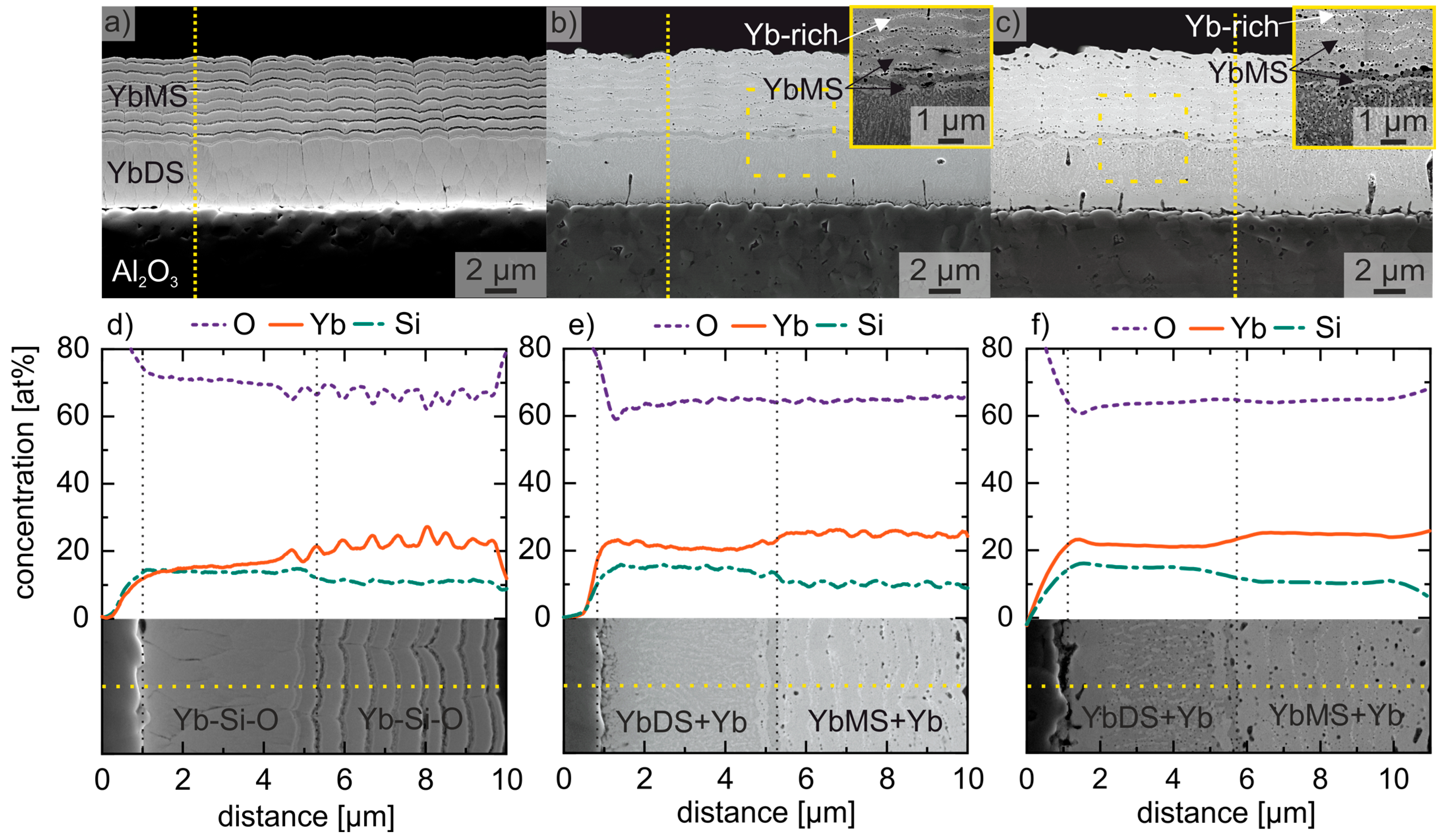
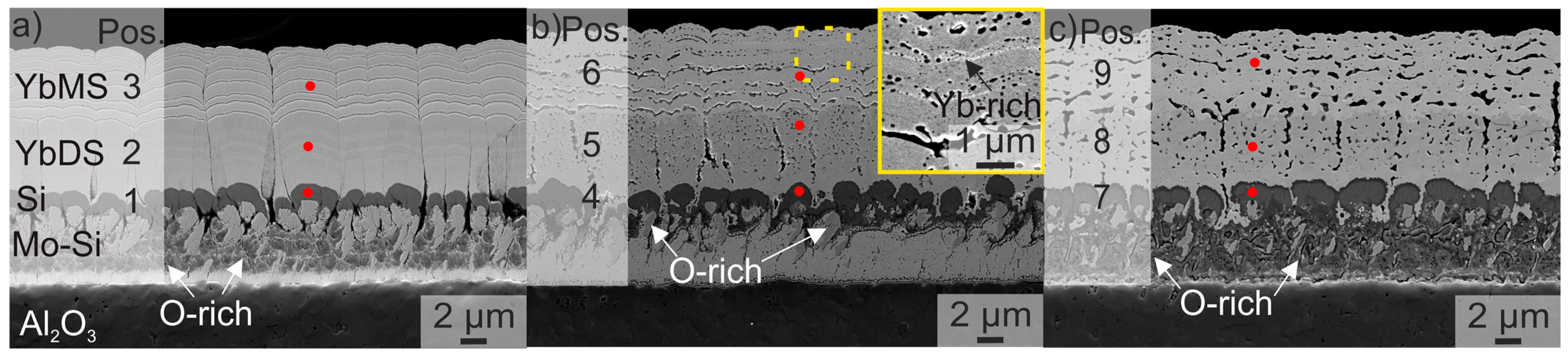
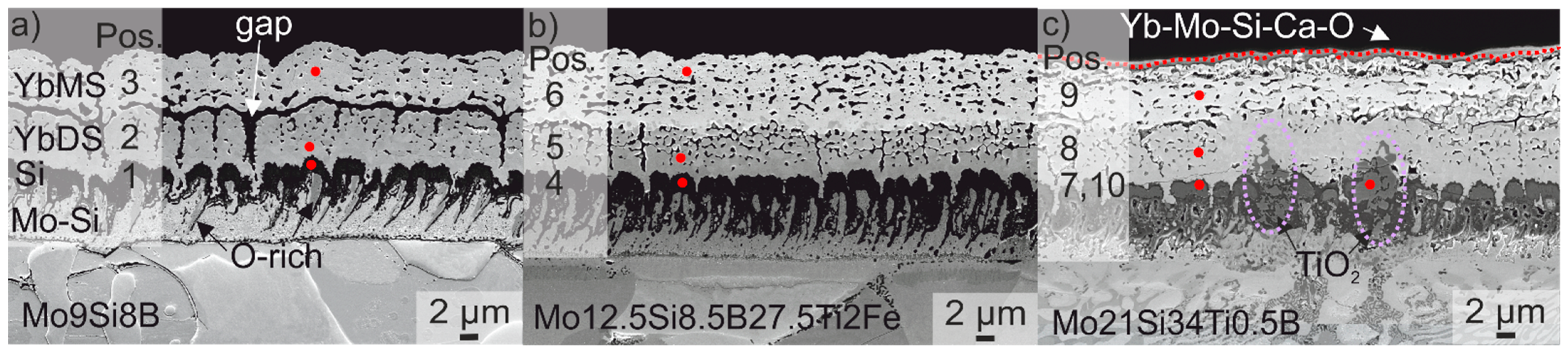
3.3. Implementation of an Yb-Silicate Based EBC System on Mo-Si-Based Alloys

In a next step, the Yb-silicate coating system was implemented on top of a graded Mo-Si interlayer with a pure Si top layer. This dual-layer coating system, hereinafter referred to as a bond coat, provides good oxidation protection on conventional and Ti-containing Mo-Si-based alloys and is therefore favoured as an interlayer system for an Yb-silicate-based EBC system. Further information about the processing by magnetron sputtering as well as the oxidation behaviour of this dual-layer system is already published in [22,24]. In the present work, the coating thickness of the pure Si top layer was intentionally reduced to 1 µm to reduce internal stresses by the CTE mismatch between the pure Si and the Mo-Si-based alloys.
In Figure 6a, the four-layered EBC system on an alumina substrate is displayed in the as-coated state. The graded Mo-Si and pure Si bond coat produced a rather rough surface; thus, the YbDS coating showed a more pronounced columnar structure with intercolumnar gaps. These columnar structures extended into the YbMS top coating. Moreover, the compositional differences of Yb and Si as mentioned above in Figure 5 were seen again on top of the bond coat. The EDS analyses revealed the right ratio for the YbDS and YbMS layer (Table 1). After the crystallisation treatment, the intercolumnar gaps within the YbDS coating were not able to be closed (Figure 6b). In the YbMS coating, the horizontal layers of a high Yb content converted into horizontal pore chains. The elemental concentration stayed stable for the Yb-silicates with a slightly higher Yb content (Table 1). After 10 h of oxidation at 1200 °C, the pore formation in the YbDS and YbMS layer increased further (Figure 6c). Nevertheless, the Yb-silicate layers on top of the bond coat showed an excellent adhesion, as did the whole EBC system on the inert substrate material of Al2O3. The oxidation of the Si layer continued, whereas the elemental concentration of the Yb-silicates remained the same.
Finally, the developed four-layered EBC coating system was deposited on three Mo-Si-based alloys: Mo-9Si-8B (at %), Mo-12.5Si-8.5B-27.5Ti-2Fe, and Mo-21Si-34Ti-0.5B. Between the Yb-silicate layers and the Mo-Si-based substrate alloys, the bond coat of graded Mo-Si and a pure Si layer was applied. In Figure 7, three different alloys were tested for 10 h at 1200 °C in air to prove the feasibility in terms of oxidation protection, adhesion and diffusion processes. Table 2 presents the EDS point analyses of the micrographs in Figure 7. Overall, the complete EBC system showed a good adhesion on all of the Mo-Si-based alloys. Compared to the inert substrate Al2O3, the pore formation in the YbDS and YbMS layer was slightly greater, especially the Yb-rich layers from deposition in the YbMS formed horizontal pore chains. In Figure 7a and b, the EBC system seemed to be less affected by the Mo-9Si-8B and Mo-12.5Si-8.5B-27.5Ti-2Fe alloy. The high contrast in these micrographs is noteworthy, where the rather black Si layer starts to oxidise in the presence of oxygen. The Yb-silicates were clearly in the range of YbDS and YbMS with a slightly higher Yb content. On the alloy Mo-21Si-34Ti-0.5B, Ti outwards diffusion took place, and as a consequence, the formation of TiO2 was observed at the interface of the bond coat and YbDS (Figure 7c and Table 2). Furthermore, a layer of 18Yb-3Mo-2.3Si-2Ca-73.5O (at %) was found on top of the whole EBC coating system deposited on the Mo-21Si-34Ti-0.5B alloy. As this layer was only found on this sample and on no other sample with the same or a different alloy, it was not investigated further. The EDS spot scans showed a partially oxidised Si layer with traces of Mo and Yb. The YbDS and YbMS layer matched the desired phases with slightly higher Yb content.
After 100 h of oxidation at 1200 °C, the EBC system on the Mo-9Si-8B still shows great oxidation protection and adhesion (Figure 8a). The Si layer of the bond coat transformed mostly into SiO2. Compared to the 10 h of testing, the EBC system did not show further pore formation. On top of the Mo-12.5Si-8.5B-27.5Ti-2Fe, SiO2 and TiO2 formed between the bond coat and YbDS (Figure 8b). The YbDS layer itself seemed denser compared to the oxidation test for 10 h. However, the two Yb-silicate layers were less distinguishable compared to Figure 7. The EBC coating system could not protect the Mo-21Si-34Ti-0.5B alloy after 100 h against oxidation (Figure 8c). The Yb-silicate coatings were still visible but disrupted. A SiO2-TiO2 mixed oxide layer grew on the surface of the alloy.
The four-layered EBC system was also tested on the three alloys at 800 °C for 100 h in air. The EBC system was able protect every alloy successfully at this temperature. In Figure 9, the result of the oxidation test was presented for the Mo-9Si-8B alloy representative because this alloy is the most prone to show the pesting phenomenon. The adhesion of the EBC system to the alloy was intact. All four layers were clearly identifiable. As seen in the figures above, the Yb-silicates developed pores in the YbDS layer vertically along the columnar gaps and in the YbMS layer horizontally with the Yb-rich microlayers. By comparing the morphology, Figure 9 seemed to be closely related to Figure 6b, where the micrograph after crystallisation was presented.

4. Discussion

4.1. Influence of the PVD Process Parameter on the Yb-Silicate Coatings

In this study, an EBC system consisting of YbDS and YbMS layers was successfully deposited by pulsed DC reactive co-sputtering. The achieved morphologies were characterised and finally tested at 1200 °C in air. The optimum operating point of the reactive sputtering process was determined in Figure 1, where the discharging curves of the Yb target for two different powers of the Yb and Si target are presented. In Figure 1a, the voltage of Si stayed stable, since it is the less reactive element used here. This is in great agreement with studies about reactive co-sputtering of Y/Yb and Si by Leisner as well as Ti and Cr by Martin et al. [17,27]. There, it was proposed that the more reactive element, here the Yb, will poison first and therefore show a hysteresis, which then presents the data to work with during deposition [17,27]. The reactivity of Yb can be attributed to the higher oxygen affinity and the heavier and lager atoms, as well as the higher sputter rate of Yb compared to Si [28,29]. As stated in Figure 1a, the Yb target started with a pure metallic eroded surface, while by increasing the oxygen flow, parts of the eroded surface formed compounds. During the transition mode, the formation and the re-sputtering of the compound is balanced out. By increasing the oxygen flow until 26 sccm, the Yb target became completely covered by an insulating compound layer. At this state, the Yb target was poisoned and therefore provided a significantly reduced sputter rate [25,30,31]. The discharging curves were executed by using different powers of 0.8 kW for Yb and 1.2 kW for Si as well as 1.2 kW for Yb and 0.9 kW for Si. The higher target power of the green curve (Yb = 1.2 kW) compared to blue curve (Yb = 0.8 kW) led to a shift of the first drop in voltage toward higher oxygen flow rates. Furthermore, the decrease in voltage of 33 % from 460 V to 305 V was double the decrease in the drop in the green curve (427 V to 367 V). The Si voltage dropped simultaneously with Yb, which could indicate that Yb can only be used in metal mode at this target power, because Si will also start poisoning at a higher oxygen flow (Figure 1b). In a study about Yb-Si and Y-Si depositions, the increase in the voltage drop and its shifting toward higher oxygen flows could be observed when using a higher target power of the more reactive element [17]. However, no decrease in the Si voltage was delivered there. According to Depla et al., the poisoning process is initiated by chemisorption if the chemical affinity of the target material to the reactive gas is high. This could be the case for Yb, based on its high electronegativity and oxygen affinity [32,33,34,35].
The aim of investigating various process parameters was to provide a sufficient reactive gas flow to deposit a layer with the desired concentration of YbDS and YbMS, containing enough oxygen without poisoning the Yb target surface. The point of interest is usually the transition mode, providing both a high deposition rate and sufficient oxygen in the layer [17,25,27,30,31,36]. Overall, studies on the reactive co-sputtering process of two cathodes with Yb and Si are rare, and the results strongly depend on the sputtering facility used [17,37].
Since the discharging curve for the deposition of the YbDS (blue curve in Figure 1a) showed a clear transition mode of Yb from 17 sccm to 24 sccm of oxygen flow, while Si remained in metallic mode, further experiments were conducted within this range at various target power ratios (Figure 2). The most predictable results and stable operating points were found at an oxygen flow of 21 sccm. A trend line could be fitted with the parameters sputtered at 21 sccm revealing the best operating point for the deposition of YbDS and YbMS (Figure 2), respectively, as in [17]. During the YbDS sputter process, the Yb target voltage increased steadily until a maximum voltage of 450 V. After that, the target voltage dropped down by about 100 V. The drop is an indicator that compounds have accumulated at the eroded target surface, signalling an initial poisoning of the Yb target, as seen in Figure 1. The drop of 100 V was about the same as the drop from 17 sccm oxygen flow (last point in metallic mode) to 21 sccm in Figure 1. This information, in conjunction with the linescan in Figure 5d, indicates that the Yb target was sputtered in transition mode at the beginning, while it changed to metallic mode at about 160 min (first light grey layer in the micrograph). The metallic mode can be assumed based on the voltage increase and on the high Yb content yet a lower oxygen content and (Figure 1a and 5d). Simultaneously, the voltage on the silicon target decreased slightly at 160 min, which is probably due to the fact that a slightly more oxygen was concentrated around the Si target. Due to the high sputter yield of Yb, the oxygen seemed to return to the target after around 6 min, transferring it from metallic into transition mode again. Although the Yb target sputtered in metallic mode, most of the atoms still reacted with the oxygen in the chamber, which is reflected by the rather decrease in oxygen content in the linescan (Figure 5d). Sputtering a target in metallic mode but still producing a fully reactive layer is possible, as shown in [38].
The deposition of the YbMS layer continued directly after the YbDS sputter process. The power of the Yb target was set to 1.15 kW, and the power of the Si target was reduced to 0.9 kW. This caused Yb to regularly switch from transition mode to metallic mode after about 15 min to 20 min, which can be followed by the voltage change of both targets. The change between the two modes continued until the end of the deposition at a surprisingly similar cycle duration, indicating a self-cleaning process of the target surface from the compound. The voltage of the Si target always decreases slightly at the highest Yb target power. Interestingly, the linescan in Figure 5d confirmed that this decrease did not transfer into a change of the Si content. At the same time, arcing on the Si target, which can be seen in the horizontal linear power and voltage drops of the target, did not lead to a change in Si concentration. The result of this unstable sputter behaviour produced a multilayer of thin Yb-rich and thicker YbMS layers. The results presented are in good agreement with Strijckmans et al., who pointed out that a small reduction in oxygen pressure can return a target from transition into metallic mode [31]. In the theoretical studies of Berg et al. on reactive co-sputtering, it is described that the composition of the coating can strongly depend on the total gas supply and that due to different reactivities between the selected target elements and the reactive gas, it might be impossible to operate two targets in metallic mode and simultaneously obtain a fully reacted coating [25]. The chosen pulsed DC power supply could also have influenced the sputtering behaviour. The benefit of a pulsed DC supply goes beyond the suppression of microarcs due to the effect of preferential sputtering. The reverse time (6 µs) and the pulse frequency (40 kHz) result in the duty cycle. The duty cycle is the coefficient of pulse frequency and the sum of pulse frequency and reverse time. How effectively this is achieved depends on the pulse rate in combination with the reversal time. In this work, a duty cycle of about 80% was used. The Yb target was able to change from transition mode to metallic mode within about 15 min to 20 min during YbMS sputtering, as shown in Figure 3. The arcing of the Si target could only be suppressed during the deposition of the YbDS coating but not during the YbMS deposition. Depla et al. described the pulsed DC supply as a discharge voltage cycles between a high negative voltage and a low positive voltage [33]. Since the negative part of the voltage causes the ions to bombard the cathode, this results in sputtering. During the low positive voltage part of the cycle, electrons are attracted to prevent a charge build-up. Due to the higher mobility of the electrons, this part of the cycle can be relatively short compared to the total cycle time [33]. A longer reverse time can result in a more efficient removal of possible target oxides during the on time, which would lead to a metallic target. In their studies, Kelly et al. [39] and Carter et al. [40] showed for aluminium oxide deposition that a duty cycle of 65 % to 70% or less is favourable for the reliable suppression of arcing [25,41,42,43].
With the selected parameters, the deposition of Yb-silicate was successfully and reproducibly enabled. The parameter selection and the process stability disclose the successful deposition of the Yb-silicates (Figure 2 and Figure 3). This study confirms that reactive sputtering is a complex and often strong nonlinear process to changes in the operation parameters or to small system fluctuations [31,33]. Further studies of the reactive co-sputtering process are needed to find optimised parameters that avoid the change in modii seen by the Yb target. To gain a deeper fundamental knowledge, the hysteresis should be investigated for both target materials separately as well. Potential solutions could involve the improvement of the pulsed DC supply by decreasing the duty cycle as studies suggested. Furthermore, the gas flow supply should be connected directly to the target voltage in order to keep the target in transition mode by simultaneously adapting the oxygen flow. A feedback system is desirable in order to balance the reactive gas and the target power or current as proposed in [31].

4.2. Influence of the Crystallisation, Morphology and Oxidation Process of an EBC Coating System on an Inert Al2O3 Substrate and Different Mo-Si-Based Alloys

Due to the applied rotation and the target arrangement during the reactive pulsed DC co-sputtering process, the coatings presented a nanolayered microstructure by alternating amorphous SiO2 and amorphous Yb2O3. The crystallisation process of the SiO2 and Yb2O3 nanolayers started in the temperature range between 480 °C and 550 °C (Figure 4). The reactive sputtering process was thereby able to provide enough oxygen so that an immediate crystallisation of the two phases could take place. It must be noted that both Yb-silicate layers were analysed at once by XRD. Therefore, the analysis represents mostly the top YbMS layer with less intense signals from the underlying YbDS. The two oxide nanolayers, Yb2O3 and SiO2, transformed between 1023 °C and 1035 °C into the stable phases β-Yb2Si2O7 and X2-Yb2SiO5. In parallel, the intensity of the silica and ytterbia peaks increased as well. Due to the higher Yb-content after the deposition process, as already seen in Figure 5d, Yb2O3 was also still measurable after the crystallisation process with less intensity compared to YbDS and YbMS. The phase formation of β-Yb2Si2O7 and X2-Yb2SiO5 continued until 1200 °C, where more peaks were identified. Despite the crystallisation temperature found in this study, We et al. could detect a thin amorphous Yb2O3 layer up to 600 °C, staying at this temperature for 60 s [44]. Pan et al. reported the crystallisation of Yb2O3 at 700 °C but without measurements taken below this temperature except for room temperature [45]. Both studies used only a few nanometer thin coatings. Garcia et al. studied the crystallisation of Yb-silicates coatings deposited by APS and were able to identify the metastable phases X1-Yb2SiO5 and α-Yb2Si2O7, as well as the stable phase β-Yb2Si2O7 at around 1000 °C, via HT-XRD. At around 1220 °C, the metastable phase of YbMS transformed into the stable phase X2-Yb2SiO5. Simultaneously, the β-phase of the YbDS replaced its metastable α-phase, and the silica peaks mostly disappeared. The formation of the metastable phase α-Yb2Si2O7 was explained by nucleation of unmelted particles of the feedstock powder [12,46,47]. The magnetron sputtering processes used in this study are known to produce clean depositions without impurities. This is largely consistent with the present results, in which no metastable phases were found. Moreover, the nanolayered structure and the stoichiometric composition of the magnetron sputtered coatings lead to possibly faster diffusion paths, which encouraged firstly the SiO2 and Yb2O3 crystallisation and the formation of the stable Yb-silicates phases.
The morphology of the amorphous Yb-silicate layers was influenced by the deposition process as explained in the subchapter above (Figure 5a). The corresponding linescan in Figure 5d indicated already after the deposition process a slightly enhanced Yb concentration overall compared to Si. Simultaneously to the Yb-rich layers, the oxygen content drops as described above. After crystallisation (Figure 5b and e), the Yb and O content homogenise over the YbDS layer with an Yb:Si ratio of about 1.5:1 and over the YbMS layer with a ratio of about 2.5:1. In the YbDS layer, the ratio led to the formation of an YbDS matrix (darker grey) with most likely YbMS precipitates (lighter grey) considering the phase diagram of Yb2O3 and SiO2 [6]. Similar phase formations were found by Garcia et al. in APS Yb-silicate coatings that had an average ratio between YbDS (39 mol %) and YbMS (61 mol %) and therefore also formed the expected phase mixture according to the phase diagram [12]. The high Yb content at the beginning of the linescan seems to be a measuring artefact because the micrograph does not mirror the result by showing only an YbDS phase (Figure 5e). Nevertheless, the Yb content overall is increased in the YbDS layer in comparison to the as-coated layer, which could be due to the diffusion processes of the Yb from the YbMS layer. There, the content homogenised as well, which agrees with the micrograph showing the Yb-rich microlayers dissolving into small chains of precipitates that most likely consist of Yb2O3 [6]. The crystallisation of the YbMS coating was accompanied by pore formation distinct in the Yb-rich layers (Figure 5b). At the interface between the YbDS and YbMS coatings, pore formation was also detected after the crystallisation process. One reason could be the necessary change in target power to deposit YbMS right after YbDS, therefore creating a short process instability. Another reason could be the different density of the two Yb-silicate phases. X2-Yb2SiO5 has a density of 7.2 g/cm3 and β-Yb2Si2O7 of 6.0 g/cm3, which leads to a different volume after crystallisation [10,47,48]. In Figure 5c,f, the homogenisation of the element contents continued with annealing time. The pore agglomeration is possibly diffusion driven and mostly noticeable at the surface of the YbMS layer and at the YbDS/YbMS interface. Nevertheless, the YbDS and YbMS layer represented themselves as hermetic dense coatings on the Al2O3 substrate, which has a low surface roughness of Ra = 0.6.
By implementing the Yb-silicates on top of the bond coat consisting of a 5 µm thick graded Mo-Si layer with a 1 µm thick Si top layer, the four-layered EBC coating system was created. The morphology changed compared to the Yb-silicates directly on the inert substrate due to different surface roughness. Although the EBC coating system was deposited on the same substrate, the bond coat created a different surface roughness for the Yb-silicates to build up on. The finger-like structure of the bond coat predesigned the columns for the YbDS. In Figure 5a, with a smooth surface, no columns could be found in the Yb-silicates, while in Figure 6a, the columns run mostly through until the surface. The phase composition matched almost perfectly the YbDS and YbMS composition, as shown in Table 1. After crystallisation, the columnar structure led to pore formation along the gaps vertically in the YbDS. At the same time, the Yb-rich microlayer within the YbMS created horizontal pore chains. Compared to Figure 5b, fewer Yb-rich precipitates in the YbMS layer and no second phase in the YbDS layer were detected. Since the composition in Figure 6b is closer to the stoichiometric YbDS and YbMS (Table 1), the Yb may have largely dissolved into the phases. Whether the effect is driven by the bond coat or due to a different sputter run cannot be determined at this point. After 10 h of oxidation (Figure 6c), a heavier pore formation could be found compared to Figure 5c. Nevertheless, the phases remained stable, and no change in composition could be detected (Table 1). The rough surface of the bond coat applied by conventional DC magnetron sputtering led to columnar gaps and thus increased the pore formation of the Yb-silicates compared to the direct deposition on the Al2O3 substrate with a low surface roughness in Figure 5.
In the last step of this study, the four-layered EBC system was applied on three Mo-Si-based alloys. After the post-crystallisation process, the EBC system was tested for 10 h and 100 h at 1200 °C and for 100 h at 800 °C in air. The micrographs of the cross-sections presented an excellent adhesion of the coating system on top of the different alloys after 10 h (Figure 8). The two Yb-silicates coating developed stable YbDS and YbMS phases, which were identifiable up to 100 h of oxidation (Table 2). The EBC system on the Mo-Si-based alloys showed the same heavy pore formation due to the surface roughness in the µm range initiated by the bond coat as seen on the inert Al2O3 substrate. Yb-rich phases were hardly found, and only the horizontal pore chains remained in the YbMS layer, which are due to the process instability. On the Mo-9Si-8B and Mo-12.5Si-8.5B-27.5Ti-2Fe alloys in Figure 8a,b, Mo was traceable within the Si/SiO2 but not within the Yb-silicates (Table 2). This suggests that Mo either did not diffuse through the Yb-silicates or diffused only in small untraceable amounts. On the Mo-12.5Si-8.5B-27.5Ti-2Fe, neither Fe nor Ti were able to diffuse into the Yb-silicate layers after 10 h. In Figure 8c, on the Mo-21Si-34Ti-0.5B, TiO2 formed between the bond coat and YbDS layer, showing that the EBC system silicates cannot provide a full oxidation protection, which is a consequence of the porosity and the oxygen diffusivity through the Yb-silicate. Moreover, Figure 8c shows the formation of a thin oxide layer on top of the YbMS containing traces of Mo, indicating that Mo from the substrate alloy or the bond coat diffused through the EBC system to the surface. In previous studies, without the Yb-silicate layers, the higher Ti content of the Mo-21Si-34Ti-0.5B alloy compared to the other alloys used and the difference in microstructure enabled Ti to diffuse fast and build TiO2 rapidly [22].
After a longer oxidation time of 100 h, the pure Si from the bond coat oxidised into a thermally grown oxide layer of SiO2 on all three alloys. On the Mo-12.5Si-8.5B-27.5Ti-2Fe alloy, TiO2 additionally formed between the bond coat and the YbDS layer (Figure 8b). In a different study, Fe could be detected within the SiO2 TGO layer, which was not found in this study after 100 h [22]. On the Mo-21Si-34Ti-0.5B alloy, the EBC system failed due to the columnar structure of the Yb-silicates accompanied by pore formation. The EBC was in this case not able to protect the alloy against oxidation (Figure 8c). This can be mainly attributed to the intentionally thinner Si layer on top of the interlayer. In the previous experiments without Yb-silicate top coatings, a thicker Si layer of around 10 µm was used, and the oxidation behaviour was much better [22]. A SiO2/TiO2 mixed oxide scale of the alloy was identified with an inhomogeneous thickness of 20 to 40 µm. Compared to the uncoated alloy in [49], where it developed an about 68 µm thick oxide scale after 100 h of isothermal oxidation at 1200 °C, the EBC coating could protect the substrate at least for a few hours against rapid oxidation. The pore formation of the Yb-silicates caused by the process fluctuations led to a layered disruption. As mentioned before, compared to oxidation studies on the bond coat consisting of the interlayer and a 10 µm thick Si top layer, the four-layered EBC system tested in this study performed worse. Only the thicker bond coat was able to protect all three alloys up to 300 h at 1200 °C [24]. Nevertheless, the four-layered EBC system shows a better adhesion than the bond coat alone on the alloys tested before, showing less spallation during cooling and therefore has great potential to act as oxidation protection. After 100 h at 800 °C, all three alloys were fully protected against the pesting phenomenon by the four-layered EBC system, as exemplarily shown for the Mo-9Si-8B alloy (Figure 9). To further improve the EBC system in a next step, the Si layer thickness has to be increased by a few µm to form a smoother surface for the deposition of the Yb-silicates and also to provide a stable oxidation and silica formation over longer times. In addition, a stable deposition process especially for the transition between YbDS and YbMS and for depositing the YbMS layer itself needs to be established to produce denser and defect-free coatings.

5. Conclusions

The reactive magnetron sputtering from two targets of Yb and Si with strongly different oxygen affinities by using pulsed DC power supplies was investigated. A first goal was therefore to investigate the process behaviour of reactive sputtering with two cathodes and to find a stable process window for the production of Yb-di and -monosilicate. The EBCs were investigated and tested on alumina substrates as well as on Mo-Si-based alloys. For the first time, a four-layered EBC system consisting of a previously developed Si-based dual layer as a bond coat [22] and separate YbDS and YbMS layers on top was manufactured and tested at 800 °C and 1200 °C in air.
The reactive co-sputtering process was more strongly influenced by Yb than by Si due to its high sputtering yield and high oxygen affinity. The Yb2Si2O7 layer was successfully deposited as an amorphous and nearly stochiometric layer. During the Yb2SiO5 deposition, the Yb target continuously switched between the metallic and transition mode, showing a self-cleaning effect and implementing locally a higher amount of Yb into the layer. This created a multilayer coating of Yb-rich and oxygen-poor microlayers within the stoichiometric Yb2SiO5 layers.
All coatings were X-ray amorphous after deposition. During crystallisation, SiO2 and Yb2O3 nanolayers formed first, which then reacted to form the stable β-Yb2Si2O7 and X2-Yb2SiO5 phases. The YbDS layer inhibited Yb-rich precipitates that are most likely Yb2SiO5 caused by a slight excess of Yb, whereas the Yb2SiO5 layer inhibited most likely Yb2O3 precipitates due to a higher overall cation ratio of Yb to Si. The volume changes during the crystallisation of the different phases as well as the fluctuation in the process stability possibly led to the formation of nanosized pores.
The impact of a high surface roughness could be shown by applying the two Yb-silicate layers on top of a Si-based rougher bond coat, where the columnar structure led to heavier pore formation. Lastly, the four-layered EBC system was applied on three different Mo-Si-based alloys. On Mo-9Si-8B (at %) and on Mo-12.5Si-8.5B-27.5Ti-2Fe, the EBCs showed great potential as oxidation protection up to 100 h at 1200 °C and on the Mo-21Si-34Ti-0.5B up to 10 h at 1200 °C. The EBC coating system could suppress the pesting phenomenon successfully until 100 h at 800 °C.
With increasing Ti content in the Mo-Si-based alloys, outward diffusion and the formation of TiO2 could only be suppressed up to 10 h for the Mo-21Si-34Ti-0.5B and up to 100 h for the Mo-12.5Si-8.5B-27.5Ti-2Fe at 1200 °C.

Author Contributions

Conceptualisation, R.A.; Funding acquisition, U.S.; Investigation, R.A.; Methodology, R.A. and V.L.; Supervision, N.L. and U.S.; Writing—original draft, R.A.; Writing—review and editing, N.L. and U.S. All authors have read and agreed to the published version of the manuscript.

Funding

This research was funded by Deutsche Forschungsgemeinschaft (DFG), grant number SCHU 1372/7-2.

Institutional Review Board Statement

Not applicable.

Informed Consent Statement

Not applicable.

Data Availability Statement

The raw and processed data required to reproduce these findings are available on request to [email protected].

Acknowledgments

The authors thank their project partners from the KIT S. Obert, A. Kauffmann and Martin Heilmaier who produced the substrate material and provided scientific support. For the scientific and technical support at the German Aerospace Center, the authors thank P.-P. Bauer, J. Brien and P. Nellessen.

Conflicts of Interest

The authors declare no conflict of interest.

References

  1. Lee, K.N. Current status of environmental barrier coatings for Si-Based ceramics. Surf. Coat. Technol. 2000, 133–134, 1–7. [Google Scholar] [CrossRef]
  2. Padture, N.P. Environmental degradation of high-temperature protective coatings for ceramic-matrix composites in gas-turbine engines. npj Mater. Degrad. 2019, 3, 11. [Google Scholar] [CrossRef] [Green Version]
  3. Tejero-Martin, D.; Bennett, C.; Hussain, T. A review on environmental barrier coatings: History, current state of the art and future developments. J. Eur. Ceram. Soc. 2021, 41, 1747–1768. [Google Scholar] [CrossRef]
  4. Bakan, E.; Marcano, D.; Zhou, D.; Sohn, Y.J.; Mauer, G.; Vaßen, R. Yb2Si2O7 Environmental Barrier Coatings Deposited by Various Thermal Spray Techniques: A Preliminary Comparative Study. J. Therm. Spray Technol. 2017, 26, 1011–1024. [Google Scholar] [CrossRef]
  5. Lee, K.N. Environmental Barrier Coatings for SiCf/SiC. In Ceramic Matrix Composites; Bansal, N.P., Lamon, J., Eds.; John Wiley & Sons: Hoboken, NJ, USA, 2014; pp. 430–451. [Google Scholar]
  6. Costa, G.C.C.; Jacobson, N.S. Mass spectrometric measurements of the silica activity in the Yb2O3–SiO2 system and implications to assess the degradation of silicate-based coatings in combustion environments. J. Eur. Ceram. Soc. 2015, 35, 4259–4267. [Google Scholar] [CrossRef]
  7. Fritsch, M. Heißgaskorrosion Keramischer Werkstoffe in H2O-Haltigen Rauchgasatmosphären; Fraunhofer IrB Verlag: Stuttgart, Germany, 2016; Volume 2. [Google Scholar]
  8. Deal, B.E.; Grove, A.S. General Relationship for the Thermal Oxidation of Silicon. J. Appl. Phys. 1965, 36, 3770–3778. [Google Scholar] [CrossRef] [Green Version]
  9. Opila, E.J. Oxidation Kinetics of Chemically Vapor-Deposited Silicon Carbide in Wet Oxygen. J. Am. Ceram. Soc. 1994, 77, 730–736. [Google Scholar] [CrossRef]
  10. Ogawa, T.; Otani, N.; Yokoi, T.; Fisher, C.A.J.; Kuwabara, A.; Moriwake, H.; Yoshiya, M.; Kitaoka, S.; Takata, M. Density functional study of the phase stability and Raman spectra of Yb2O3, Yb2SiO5 and Yb2Si2O7 under pressure. Phys. Chem. Chem. Phys. 2018, 20, 16518–16527. [Google Scholar] [CrossRef]
  11. Richards, B.T.; Wadley, H.N.G. Plasma spray deposition of tri-layer environmental barrier coatings. J. Eur. Ceram. Soc. 2014, 34, 3069–3083. [Google Scholar] [CrossRef]
  12. Garcia, E.; Sotelo-Mazon, O.; Poblano-Salas, C.A.; Trapaga, G.; Sampath, S. Characterization of Yb2Si2O7–Yb2SiO5 composite environmental barrier coatings resultant from in situ plasma spray processing. Ceram. Int. 2020, 46, 21328–21335. [Google Scholar] [CrossRef]
  13. Chen, H.; Gao, Y.; Liu, Y.; Luo, H. Hydrothermal synthesis of ytterbium silicate nanoparticles. Inorg. Chem. 2010, 49, 1942–1946. [Google Scholar] [CrossRef] [PubMed]
  14. Zhong, X.; Niu, Y.R.; Li, H.; Zhou, H.J.; Dong, S.M.; Zheng, X.B.; Ding, C.X.; Sun, J.L. Thermal shock resistance of tri-layer Yb2SiO5/Yb2Si2O7/Si coating for SiC and SiC-matrix composites. J. Am. Ceram. Soc. 2018, 101, 4743–4752. [Google Scholar] [CrossRef]
  15. Richards, B.T.; Young, K.A.; de Francqueville, F.; Sehr, S.; Begley, M.R.; Wadley, H.N.G. Response of ytterbium disilicate–silicon environmental barrier coatings to thermal cycling in water vapor. Acta Mater. 2016, 106, 1–14. [Google Scholar] [CrossRef] [Green Version]
  16. Bakan, E.; Sohn, Y.J.; Kunz, W.; Klemm, H.; Vaßen, R. Effect of processing on high-velocity water vapor recession behavior of Yb-silicate environmental barrier coatings. J. Eur. Ceram. Soc. 2019, 39, 1507–1513. [Google Scholar] [CrossRef]
  17. Leisner, V. Neue Environmental Barrier Coatings für SiC/SiC-Faserverbundwerkstoffe durch PVD-Technologien. Ph.D. Thesis, Karlsruher Institut für Technologie (KIT), Karlsruhe, Germany, 2020. [Google Scholar]
  18. Leisner, V.; Kelm, K.; Schulz, U. Thin single-phase yttrium-based environmental barrier coating systems for SiC/SiC CMCs. J. Eur. Ceram. Soc. 2022. (submitted and under review). [Google Scholar]
  19. Obert, S. Characterisation of the Oxidation and Creep Behaviour of Novel Mo-Si-Ti Alloys. Ph.D. Thesis, Karlsruher Institut für Technologie (KIT), Karlsruhe, Germany, 2021. [Google Scholar]
  20. Obert, S.; Kauffmann, A.; Seils, S.; Boll, T.; Kauffmann-Weiss, S.; Chen, H.; Anton, R.; Heilmaier, M. Microstructural and chemical constitution of the oxide scale formed on a pesting-resistant Mo-Si-Ti alloy. Corros. Sci. 2021, 178, 109081. [Google Scholar] [CrossRef]
  21. Lange, A.; Braun, R.; Heilmaier, M. Oxidation behavior of magnetron sputtered double layer coatings containing molybdenum, silicon and boron. Intermetallics 2014, 48, 19–27. [Google Scholar] [CrossRef]
  22. Anton, R.; Hüning, S.; Laska, N.; Weber, M.; Schellert, S.; Gorr, B.; Christ, H.-J.; Heilmaier, M.; Schulz, U. Interface reactions of magnetron sputtered Si-based dual layer coating systems as oxidation protection for Mo-Si-Ti alloys. Surf. Coat. Technol. 2022, 444, 128620. [Google Scholar] [CrossRef]
  23. Anton, R.; Laska, N.; Schulz, U.; Obert, S.; Heilmaier, M. Magnetron Sputtered Silicon Coatings as Oxidation Protection for Mo-Based Alloys. Adv. Eng. Mater. 2020, 22, 2000218. [Google Scholar] [CrossRef]
  24. Anton, R.; Hüning, S.; Laska, N.; Weber, M.; Schellert, S.; Gorr, B.; Christ, H.-J.; Schulz, U. Graded PVD Mo-Si interlayer between Si coating and Mo-Si-B alloys: Investigation of oxidation behaviour. Corros. Sci. 2021, 192, 109843. [Google Scholar] [CrossRef]
  25. Berg, S.; Nyberg, T. Fundamental understanding and modeling of reactive sputtering processes. Thin Solid Film 2005, 476, 215–230. [Google Scholar] [CrossRef]
  26. Spencer, S. Table of Argon Sputtering Yields at 0°; National Physical Laboratory: London, UK, 2005. [Google Scholar]
  27. Martin, N.; Rousselot, C. Modelling of reactive sputtering processes involving two separated metallic targets. Surf. Coat. Technol. 1999, 114, 235–249. [Google Scholar] [CrossRef]
  28. Liang, J.-J.; Navrotsky, A.; Ludwig, T.; Seifert, H.J.; Aldinger, F. Enthalpy of Formation of Rare-earth Silicates Y2SiO5 and Yb2SiO5 and N-containing Silicate Y10(SiO4)6N2. J. Mater. Res. 1999, 14, 1181–1185. [Google Scholar] [CrossRef]
  29. Miyazaki, T.; Usami, S.; Inoue, R.; Kogo, Y.; Arai, Y. Oxidation behavior of ytterbium silicide. Ceram. Int. 2019, 45, 9560–9566. [Google Scholar] [CrossRef]
  30. Depla, D.; Heirwegh, S.; Mahieu, S.; Haemers, J.; Gryse, R.D. Understanding the discharge voltage behavior during reactive sputtering of oxides. J. Appl. Phys. 2007, 101, 013301. [Google Scholar] [CrossRef]
  31. Strijckmans, K.; Schelfhout, R.; Depla, D. Tutorial: Hysteresis during the reactive magnetron sputtering process. J. Appl. Phys. 2018, 124, 241101. [Google Scholar] [CrossRef]
  32. Depla, D.; De Gryse, R. Target poisoning during reactive magnetron sputtering: Part III: The prediction of the critical reactive gas mole fraction. Surf. Coat. Technol. 2004, 183, 196–203. [Google Scholar] [CrossRef]
  33. Depla, D.; Mahieu, S.; Greene, J.E. Chapter 5—Sputter Deposition Processes. In Handbook of Deposition Technologies for Films and Coatings, 3rd ed.; Martin, P.M., Ed.; William Andrew Publishing: Boston, MA, USA, 2010; pp. 253–296. [Google Scholar]
  34. Xia, X.; Qiu, P.; Shi, X.; Li, X.; Huang, X.; Chen, L. High-Temperature Oxidation Behavior of Filled Skutterudites YbyCo4Sb12. J. Electron. Mater. 2012, 41, 2225–2231. [Google Scholar] [CrossRef]
  35. Toberer, E.S.; May, A.F.; Melot, B.C.; Flage-Larsen, E.; Snyder, G.J. Electronic structure and transport in thermoelectric compounds AZn2Sb2 (A = Sr, Ca, Yb, Eu). Dalton Trans. 2010, 39, 1046–1054. [Google Scholar] [CrossRef] [Green Version]
  36. Mattox, D.M. Handbook of Physical Vapor Deposition (PVD) Processing, 2nd ed.; William Andrew Publishing: Boston, MA, USA, 2010. [Google Scholar]
  37. Berg, S.; Särhammar, E.; Nyberg, T. Upgrading the “Berg-model” for reactive sputtering processes. Thin Solid Films 2014, 565, 186–192. [Google Scholar] [CrossRef]
  38. Lei, P.; Leroy, W.; Dai, B.; Zhu, J.; Chen, X.; Han, J.; Depla, D. Study on reactive sputtering of yttrium oxide: Process and thin film properties. Surf. Coat. Technol. 2015, 276, 39–46. [Google Scholar] [CrossRef]
  39. Kelly, P.J.; Henderson, P.S.; Arnell, R.D.; Roche, G.A.; Carter, D. Reactive pulsed magnetron sputtering process for alumina films. J. Vac. Sci. Technol. A 2000, 18, 2890–2896. [Google Scholar] [CrossRef]
  40. Carter, D.; Walde, H.; McDonough, G.; Roche, G. Parameter Optimization in Pulsed DC Reactive Sputter Deposition of Aluminum Oxide. In Proceedings of the 45th Annual Technical Conference of the Society of Vauum Coaters, Lake Buena Vista, FL, USA, 15–16 April 2002; pp. 570–577. [Google Scholar]
  41. Sproul, W.D.; Christie, D.J.; Carter, D.C. Control of reactive sputtering processes. Thin Solid Films 2005, 491, 1–17. [Google Scholar] [CrossRef]
  42. Sellers, J. Asymmetric bipolar pulsed DC: The enabling technology for reactive PVD. Surf. Coat. Tech. 1998, 98, 1245–1250. [Google Scholar] [CrossRef]
  43. Belkind, A.; Zhao, Z.; Carter, D.; Mahoney, L.; McDonough, G.; Roche, G.; Scholl, R.; Walde, H. Pulsed-DC Reactive Sputtering of Dielectrics: Pulsing Parameter Effects. In Proceedings of the 43rd Annual Technical Conference Proceedings, Denver, CO, USA, 15–20 April 2000; pp. 86–90. [Google Scholar]
  44. Wu, M.-L.; Wu, Y.-H.; Chao, C.-Y.; Lin, C.-C.; Wu, C.-Y. Crystalline ZrTiO4-Gated Ge Metal–Oxide–Semiconductor Devices With Amorphous Yb2O3 as a Passivation Layer. IEEE Trans. Nanotechnol. 2013, 12, 1018–1021. [Google Scholar] [CrossRef]
  45. Pan, T.-M.; Cheng, C.-H.; Lee, C.-D. Yb2O3 Thin Films as a Sensing Membrane for pH-ISFET Application. J. Electrochem. Soc. 2009, 156, J108. [Google Scholar] [CrossRef]
  46. Garcia, E.; Lee, H.; Sampath, S. Phase and microstructure evolution in plasma sprayed Yb2Si2O7 coatings. J. Eur. Ceram. Soc. 2019, 39, 1477–1486. [Google Scholar] [CrossRef]
  47. Garcia, E.; Garces, H.F.; Turcer, L.R.; Bale, H.; Padture, N.P.; Sampath, S. Crystallization behavior of air-plasma-sprayed ytterbium-silicate-based environmental barrier coatings. J. Eur. Ceram. Soc. 2021, 41, 3696–3705. [Google Scholar] [CrossRef]
  48. Ridley, M.; Opila, E. Thermochemical stability and microstructural evolution of Yb2Si2O7 in high-velocity high-temperature water vapor. J. Eur. Ceram. Soc. 2021, 41, 3141–3149. [Google Scholar] [CrossRef]
  49. Schliephake, D.; Kauffmann, A.; Cong, X.; Gombola, C.; Azim, M.; Gorr, B.; Christ, H.-J.; Heilmaier, M. Constitution, oxidation and creep of eutectic and eutectoid Mo-Si-Ti alloys. Intermetallics 2019, 104, 133–142. [Google Scholar] [CrossRef]
Figure 1. Discharge behaviour of the Yb and Si target plotted as ratio of the actual voltage to the initial voltage w/o reactive gas during the successive increase in oxygen flow at a total pressure of 4 × 10⁻³ mbar; (a) represents a power ratio that targets the YbDS composition; (b) represents a power ratio that targets the YbMS composition.
Coatings 12 01086 g001
Figure 2. Parameter selection with different oxygen flow rates represented by the cation ratio of Yb and Si (measured by EDS) as a function of the power ratio of Yb and Si. The green line represents the YbMS cation ratio; the blue line represents the YbDS cation ratio. Each run is represented by the square symbol, where the cYb/cSi ratio was analysed and the oxygen concentration was measured and colour coded. The red circles around the squares represent the parameters with a 21 sccm O2 flow rate, while all other points were achieved using a 5 sccm to 29 sccm O2 flow rate. The dotted line is a linear fit of the results using 21 sccm O2. The red crosses indicate the right target power ratio for the YbDS and YbMS coating.
Coatings 12 01086 g002
Figure 3. Process data of YbDS and YbMS coating by reactive magnetron sputtering and underlying the micrograph of the as-coated microstructure on an Al2O3 substrate.
Coatings 12 01086 g003
Figure 4. HT-XRD scans of the YbDS and YbMS coating on an Al2O3 substrate; (a) contour colour plot of one-minute scans from 10°–60° starting at 30 °C followed by 1 h at 900 °C and 1 h at 1200 °C in air; (b) X-ray scans in the as-coated state at 30 °C, during 1 h at 900 °C, during 1 h at 1200 °C and after cooling down in the crystallised state to 30 °C.
Coatings 12 01086 g004
Figure 5. Secondary electron SEM micrographs of the Yb-silicate coatings on an Al2O3 substrate; (a) after the deposition process in the as-coated state; (b) after crystallisation treatment for 1 h at 900 °C followed by 1 h at 1200 °C in lab air; (c) after an additional 10 h of oxidation testing at 1200 °C in lab air. EDS linescan with secondary electron micrographs of the Yb-silicate coatings on top of an Al2O3 substrate; (d) after deposition in the as-coated state; (e) after crystallisation for one hour at 900 °C and one hour at 1200 °C in air; (f) after 10 h of oxidation test at 1200 °C.
Coatings 12 01086 g005
Figure 6. Secondary electron SEM micrographs of the dual-layer bond coat and the YbDS and YbMS EBC coatings on top of an Al2O3 substrate; (a) after deposition in the as-coated state; (b) after crystallisation for 1 h at 900 °C plus 1 h at 1200 °C in air; (c) after additional 10 h of oxidation test at 1200 °C with positions marked by red dots for different EDS spot analyses represented in Table 1.
Coatings 12 01086 g006
Figure 7. Secondary electron SEM micrographs of the dual-layer bond coat and the YbDS and YbMS top layer on (a) Mo-9Si-8B alloy, (b) Mo-12.5Si-8.5B-27.5Ti-2Fe alloy, (c) Mo-21Si-34Ti-0.5B alloy after 10 h of oxidation test at 1200 °C in air with a position marked by red dots for different EDS spot analyses represented in Table 2.
Coatings 12 01086 g007
Figure 8. Secondary electron SEM micrographs of the bond coat and the YbDS and YbMS top layer on (a) Mo-9Si-8B alloy, (b) Mo-12.5Si-8.5B-27.5Ti-2Fe alloy, (c) Mo-21Si-34Ti-0.5B alloy after 100 h of oxidation test at 1200 °C in air.
Coatings 12 01086 g008
Figure 9. Secondary electron SEM micrographs of the bond coat and the YbDS and YbMS top layer on Mo-9Si-8B alloy after 100 h of oxidation test at 800 °C in air.
Coatings 12 01086 g009
Table 1. EDS spot analyses in the marked red dots in Figure 6.
as-CoatedCrystallised10 h at 1200 °C
Position123456789
Yb (at %)1.416.522.22.018.123.21.015.521.8
Si (at %)82.614.810.679.515.19.661.014.310.7
Mo (at %)2.7002.0001.600
O (at %)13.368.667.216.565.866.236.470.267.5
Table 2. EDS spot analyses in the red dots marked in Figure 7.
Mo9Si8BMo12.5Si8.5B27.5Ti2FeMo21Si34Ti0.5B
Position12345678910
Yb (at %)0.916.021.41.319.022.01.819.524.00
Si (at %)72.216.010.565.216.111.072.915.411.01.8
Mo (at %)2.3001.5001.1000.4
Ti (at %)---00000032.3
O (at %)24.668.068.132.064.967.024.265.165.065.5
Publisher’s Note: MDPI stays neutral with regard to jurisdictional claims in published maps and institutional affiliations.

