
A Study on the Gap-Fill Process Deposited by the Deposition/Etch/Deposition Method in the Space-Divided PE-ALD System

Abstract
:1. Introduction
2. Experiments and Discussion
2.1. Experimental Method
2.1.1. Development of the Experimental Equipment
2.1.2. Deposition Process
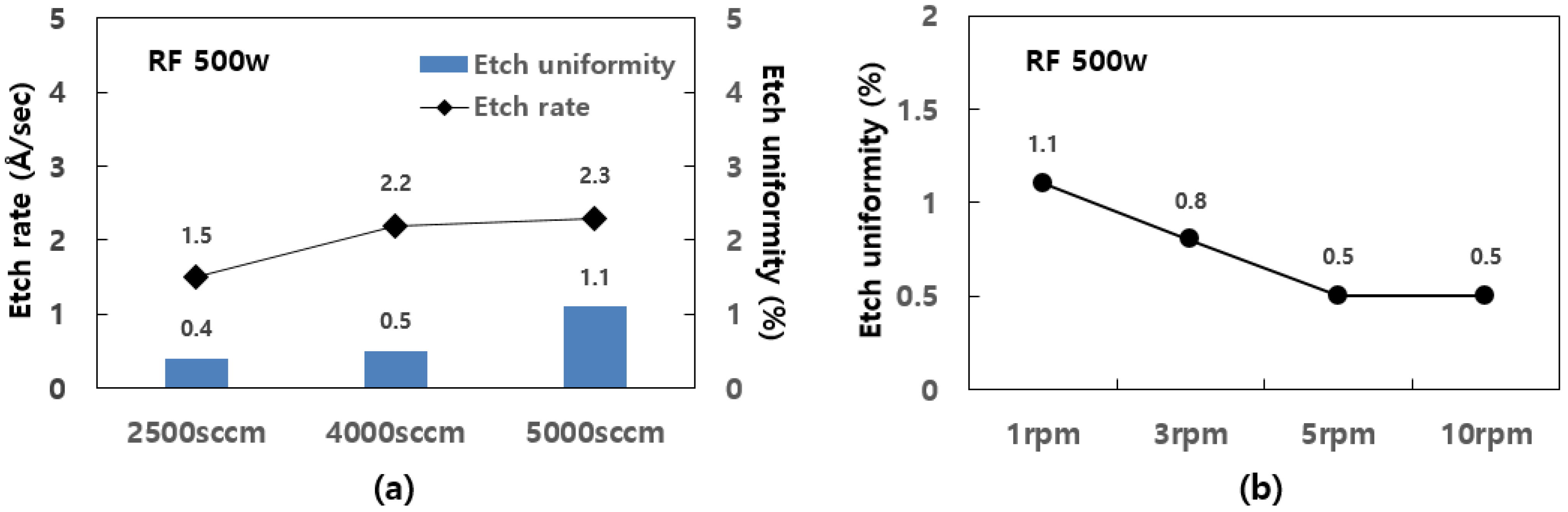
2.1.3. Etch Process
2.1.4. Analysis Method
2.2. The Deposition/Etch/Deposition Process Development
2.2.1. Silicon Oxide Thin Film Deposited by the PE-ALD Method
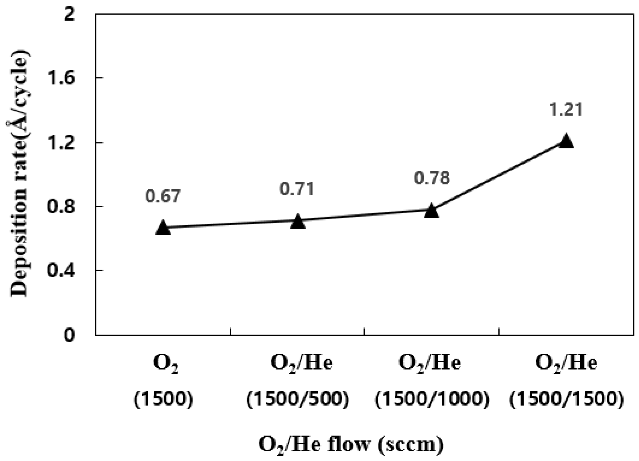
2.2.2. DED Process Method
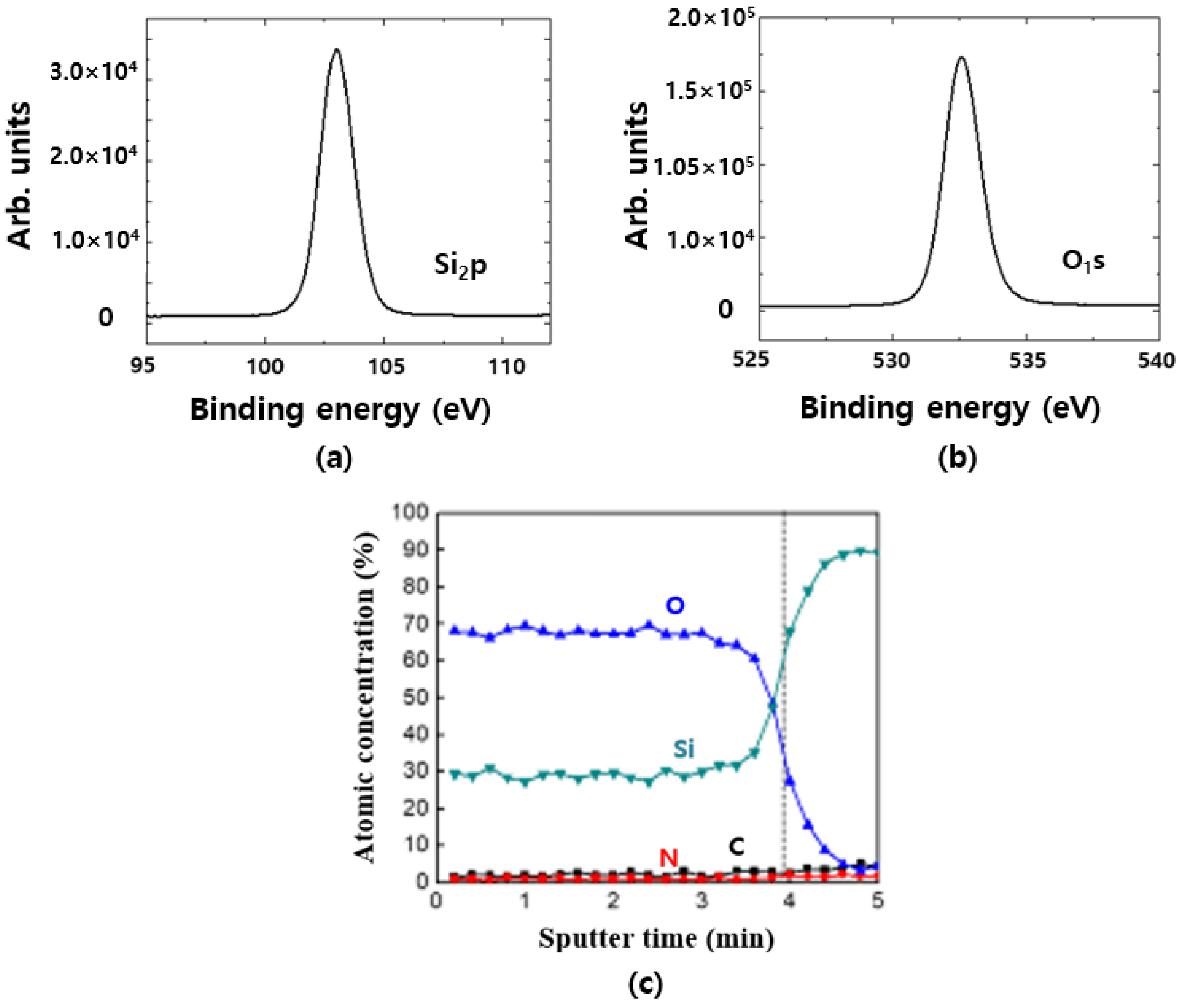
2.2.3. Fluorine Analysis of SiO2 Thin Film Deposited by the DED Process
2.2.4. Electrical Characteristics’ Analysis of SiO2 Thin Film Deposited by the DED Process
- -
- area = 100 × 100 (µm2)
- -
- Ɛo = 8.8542 × 10⁻¹² F/m
- -
- k = dielectric constant

2.3. Deposition/Etch/Deposition Process in the Pattern
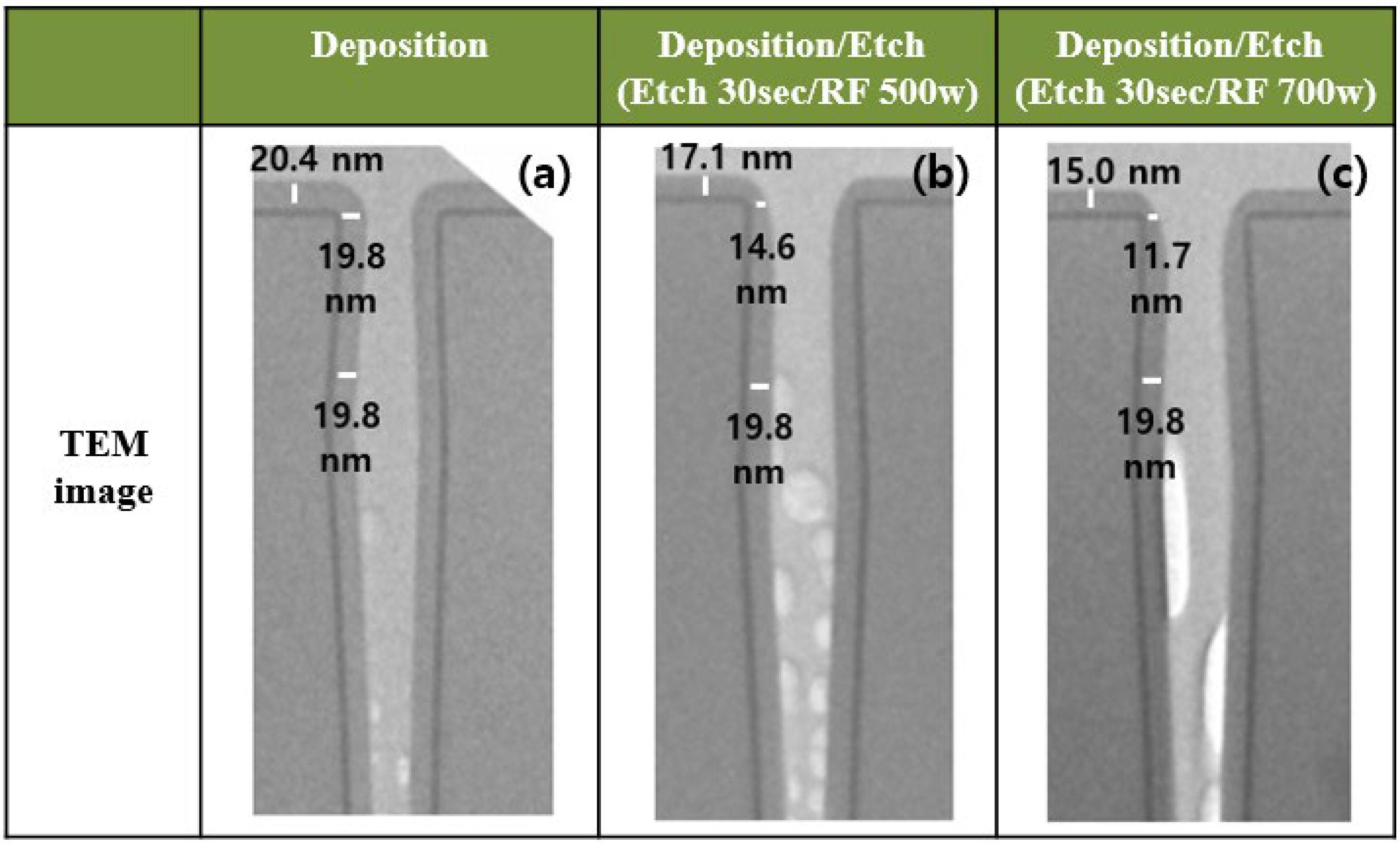
2.3.1. Evaluation of Etch Influence in the Pattern
2.3.2. Gap-Fill Evaluation in High Aspect Ratio Pattern
3. Conclusions
Author Contributions
Funding
Institutional Review Board Statement
Informed Consent Statement
Data Availability Statement
Conflicts of Interest
References
- Lee, B.; Hwang, J.; Seo, D.; Choi, J. Development of space divided PE-ALD system and process design for gap-fill process in advanced memory devices. J. Korean Inst. Surf. Eng. 2020, 53, 124–129. [Google Scholar]
- Grillo, F.; Soethoudt, J.; Marques, E.A. Area-selective deposition of ruthenium by area-dependent surface diffusion. Chem. Mater. 2020, 32, 9560–9572. [Google Scholar] [CrossRef]
- Khan, R.; Shong, B.; Ko, B.G.; Lee, J.K.; Lee, H.; Park, J.Y.; Oh, I.-K.; Raya, S.S.; Hong, H.M.; Chung, K.-B.; et al. Area-selective atomic layer deposition using Si precursors as inhibitors. Chem. Mater. 2018, 30, 7603–7610. [Google Scholar] [CrossRef]
- Nam, T.; Lee, H.; Choi, T. Low-temperature, high-growth-rate ALD of SiO2 using aminodisilane precursor. Appl. Surf. Sci. 2019, 485, 381–390. [Google Scholar] [CrossRef]
- Jeong, S.H.; Kim, J.K.; Kim, B.S.; Shim, S.H.; Lee, B.T. Characterization of SiO2 and TiO2 films prepared using rf magnetron sputtering and their application to anti-reflection coating. Vacuum 2004, 76, 507–515. [Google Scholar] [CrossRef]
- Gabriel, N.T.; Kim, S.S.; Talghader, J.J. Control of thermal deformation in dielectric mirrors using mechanical design and atomic layer deposition. Opt. Lett. 2009, 34, 1958–1960. [Google Scholar] [CrossRef]
- Lee, B.-J.; Seo, D.-W.; Choi, J.-W. Analysis of the influence of disk and wafer rotation speed on the SiO2 thin-film characteristics in a space-divided PE-ALD system. J. Korean Phys. Soc. 2021, 79, 638–647. [Google Scholar] [CrossRef]
- Lee, B.; Seo, D.; Choi, J.-W. Effect of reactive gases (NH3/N2) on silicon–nitride thin films deposited with diiodosilane (SiH2I2) precursors. JKPS 2022, 80, 311–319. [Google Scholar] [CrossRef]
- Sneh, O.; Wise, M.; Ott, A.; Okada, L.; George, S. Atomic layer growth of SiO2 on Si(100) using SiCl4 and H2O in a binary reaction sequence. Surf. Sci. 1995, 334, 135–152. [Google Scholar] [CrossRef]
- Degai, M.; Kanomata, K.; Momiyama, K.; Kubota, S.; Hirahara, K.; Hirose, F. Non-heating atomic layer deposition of SiO2 using tris(dimethylamino)silane and plasma-excited water vapor. Thin Solid Films 2012, 525, 73–76. [Google Scholar] [CrossRef]
- Kamiyama, S.; Miura, T.; Nara, Y. Comparison between SiO2 films deposited by atomic layer deposition with SiH2[N(CH3)2]2 and SiH[N(CH3)2]3 precursors. Thin Solid Films 2006, 515, 1517–1521. [Google Scholar] [CrossRef]
- Miikkulainen, V.; Leskela, M.; Ritala, M.; Puurunen, R.L. Crystallinity of inorganic films grown by atomic layer deposition: Overview and general trends. J. Appl. Phys. 2013, 113, 21301. [Google Scholar] [CrossRef]
- Burton, B.B.; Kang, S.W.; Rhee, S.W.; George, S.M. SiO2 Atomic layer deposition using tris(dimethylamino)silane and hydrogen peroxide studied by in situ transmission FTIR spectroscopy. J. Phys. Chem. C 2009, 113, 8249–8257. [Google Scholar] [CrossRef]
- Kobayashi, A.; Tsuji, N.; Fukazawa, A.; Kobayashi, N. Temperature dependence of SiO2 film growth with plasma-enhanced atomic layer deposition. Thin Solid Films 2012, 520, 3994–3998. [Google Scholar] [CrossRef]
- Dingemans, G.; van Helvoirt, C.A.A.; Pierreux, D.; Keuning, W.; Kessels, W.M.M. Plasma-assisted ALD for the conformal deposition of SiO2: Process, material and electronic propertie. J. Electrochem. Soc. 2012, 159, 277–285. [Google Scholar] [CrossRef] [Green Version]
- Choi, J.S.; Yang, B.S.; Won, S.J.; Kim, J.R.; Suh, S.; Park, H.K.; Heo, J.; Kim, H.J. Low temperature formation of silicon oxide thin films by atomic layer deposition using NH3/O2-plasma. Electrochem. Solid State 2013, 2, 114–116. [Google Scholar] [CrossRef]
- Putkonen, M.; Bosund, M.; Ylivaara, O.M.; Puurunen, R.L.; Kilpi, L.; Ronkainen, H.; Sintonen, S.; Ali, S.; Lipsanen, H.; Liu, X.; et al. Thermal and plasma enhanced atomic layer deposition of SiO2 using commercial silicon precursors. Thin Solid Films 2014, 558, 93–98. [Google Scholar] [CrossRef]
- Schmidt, J.; Merkle, A.; Brendel, R.; Hoex, B.; van de Sanden, M.C.M.; Kessels, W.M.M. Surface passivation of high-efficiency silicon solar cells by atomic-layer-deposited Al2O3. Prog. Photovolt. Res. Appl. 2008, 16, 461–466. [Google Scholar] [CrossRef]
- Ratzsch, S.; Kley, E.-B.; Tünnermann, A.; Szeghalmi, A. Inhibition of crystal growth during plasma enhanced atomic layer deposition by applying BIAS. Materials 2015, 8, 7805–7812. [Google Scholar] [CrossRef] [Green Version]
- Song, S.J.; Lee, S.W.; Kim, G.-H.; Seok, J.Y.; Yoon, K.J.; Yoon, J.H.; Hwang, C.S.; Gatineau, J.; Ko, C. Substrate dependent growth behaviors of plasma-enhanced atomic layer deposited nickel oxide films for resistive switching application. Chem. Mater. 2012, 24, 4675–4685. [Google Scholar] [CrossRef]
- Xie, J.; Yang, X.; Han, B.; Shao-Horn, Y.; Wang, D. Site-selective deposition of twinned Pt nanoparticles on TiSi2 nanonets by atomic layer deposition and their oxygen reduction activities. ACS Nano 2013, 7, 6337–6345. [Google Scholar] [CrossRef] [PubMed]
- Lee, H.-B.; Baeck, S.H.; Jaramillo, T.F.; Bent, S.F. Growth of Pt nanowires by atomic layer deposition on highly ordered pyrolytic graphite. Nano Lett. 2013, 13, 457–463. [Google Scholar] [CrossRef] [PubMed]
- Chen, R.; Bent, S.F. Chemistry for positive pattern transfer using area-selective atomic layer deposition. Adv. Mater. 2006, 18, 1086–1090. [Google Scholar] [CrossRef]
- Watanabe, T.; Goto, N.; Yasuhisa, N.; Yanase, T.; Tanaka, T.; Shinozaki, S. Highly reliable trench capacitor with SiO2/Si3N4/SiO2 stacked film. In Proceedings of the 25th International Reliability Physics Symposium, San Diego, CA, USA, 7–9 April 1987; pp. 50–54. [Google Scholar]
- Robertson, J.; Wallace, R.M. High-K materials and metal gates for CMOS applications. Mater. Sci. Eng. R Rep. 2015, 88, 1–41. [Google Scholar] [CrossRef] [Green Version]
- Endo, K.; Ishikawa, Y.; Matsukawa, T.; Liu, Y.; O’Uchi, S.-I.; Sakamoto, K.; Tsukada, J.; Yamauchi, H.; Masahara, M. Atomic layer deposition of SiO2 for the performance enhancement of fin field effect transistors. Jpn. J. Appl. Phys. 2013, 52, 116503. [Google Scholar] [CrossRef]
- Won, S.-J.; Suh, S.; Huh, M.S.; Kim, H.J. High-quality low-temperature silicon oxide by plasma-enhanced atomic layer deposition using a metal–organic silicon precursor and oxygen radical. IEEE Electron. Device Lett. 2010, 31, 857–859. [Google Scholar]
- Han, B.; Zhang, Q.; Wu, J.; Han, B.; Karwacki, E.J.; Derecskei, A.; Xiao, M.; Lei, X.; O’Neill, M.L.; Cheng, H. On the mechanisms of SiO2 thin-film growth by the full atomic layer deposition process using bis(t-butylamino)silane on the hydroxylated SiO2(001) Surface. J. Phys. Chem. C 2012, 116, 947–952. [Google Scholar] [CrossRef]
- Huang, L.; Han, B.; Han, B.; Derecskei-Kovacs, A.; Xiao, M.; Lei, X.; O’Neill, M.L.; Pearlstein, R.M.; Chandra, H.; Cheng, H. First-principles study of a full cycle of atomic layer deposition of SiO2 thin films with di(sec-butylamino)silane and ozone. J. Phys. Chem. C 2013, 117, 19454–19463. [Google Scholar]
- Jung, H.; Kim, W.-H.; Oh, I.-K.; Lee, C.-W.; Lansalot-Matras, C.; Lee, S.J.; Myoung, J.-M.; Lee, H.-B.-R.; Kim, H. Growth characteristics and electrical properties of SiO2 thin films prepared using plasma-enhanced atomic layer deposition and chemical vapor deposition with an aminosilane precursor. J. Mater. Sci. 2016, 51, 5082–5091. [Google Scholar] [CrossRef]
- Ahn, S.; Kim, Y.; Kang, S.; Im, K.; Lim, H. Low-temperature-atomic-layer-deposition of SiO2 using various organic precursors. J. Vac. Sci. Technol. A 2017, 35, 01B131. [Google Scholar] [CrossRef]
- Choi, Y.-J.; Bae, S.-M.; Kim, J.-H.; Kim, E.-H.; Hwang, H.-S.; Park, J.-W.; Yang, H.; Choi, E.; Hwang, J.-H. Robust SiO2 gate dielectric thin films prepared through plasma-enhanced atomic layer deposition involving di-sopropylamino silane (DIPAS) and oxygen plasma: Application to amorphous oxide thin film transistors. Ceram. Int. 2018, 44, 1556–1565. [Google Scholar] [CrossRef]
- O’Neill, M.L.; Bowen, H.R.; Derecskei-Kovacs, A.; Cuthill, K.S.; Han, B.; Xiao, M. Impact of aminosilane precursor structure on silicon oxides by atomic layer deposition. Electrochem. Soc. Interface 2011, 20, 33–37. [Google Scholar] [CrossRef] [Green Version]
- Kim, W.-H.; Oh, I.-K.; Kim, M.-K.; Maeng, W.J.; Lee, C.-W.; Lee, G.; Lansalot-Matras, C.; Noh, W.; Thompson, D.; Chu, D.; et al. Atomic layer deposition of B2O3/SiO2 thin films and their application in an efficient diffusion doping process. J. Mater. Chem. C 2014, 2, 5805–5811. [Google Scholar] [CrossRef]
- Ferguson, J.D.; Smith, E.R.; Weimer, A.W.; George, S.M. ALD of SiO2 at room temperature using TEOS and H2O with NH3 as the Catalyst. J. Electrochem. Soc. 2004, 151, G528–G535. [Google Scholar] [CrossRef]
- Klaus, J.W.; Sneh, O.; George, S.M. Growth of SiO2 at room temperature with the use of catalyzed sequential half-reactions. Science 1997, 278, 1934–1936. [Google Scholar] [CrossRef]


Disclaimer/Publisher’s Note: The statements, opinions and data contained in all publications are solely those of the individual author(s) and contributor(s) and not of MDPI and/or the editor(s). MDPI and/or the editor(s) disclaim responsibility for any injury to people or property resulting from any ideas, methods, instructions or products referred to in the content. |
© 2022 by the authors. Licensee MDPI, Basel, Switzerland. This article is an open access article distributed under the terms and conditions of the Creative Commons Attribution (CC BY) license (https://creativecommons.org/licenses/by/4.0/).
Share and Cite
Lee, B.-J.; Seo, D.-W.; Choi, J.-W. A Study on the Gap-Fill Process Deposited by the Deposition/Etch/Deposition Method in the Space-Divided PE-ALD System. Coatings 2023, 13, 48. https://doi.org/10.3390/coatings13010048
Lee B-J, Seo D-W, Choi J-W. A Study on the Gap-Fill Process Deposited by the Deposition/Etch/Deposition Method in the Space-Divided PE-ALD System. Coatings. 2023; 13(1):48. https://doi.org/10.3390/coatings13010048
Chicago/Turabian StyleLee, Baek-Ju, Dong-Won Seo, and Jae-Wook Choi. 2023. "A Study on the Gap-Fill Process Deposited by the Deposition/Etch/Deposition Method in the Space-Divided PE-ALD System" Coatings 13, no. 1: 48. https://doi.org/10.3390/coatings13010048
APA StyleLee, B.-J., Seo, D.-W., & Choi, J.-W. (2023). A Study on the Gap-Fill Process Deposited by the Deposition/Etch/Deposition Method in the Space-Divided PE-ALD System. Coatings, 13(1), 48. https://doi.org/10.3390/coatings13010048