
Synthesis and Characterization of Amorphous Selenium, Cadmium and Silver Selenide Thin Films on Polyamide-6

Abstract
:1. Introduction
2. Materials and Methods
3. Results and Discussions
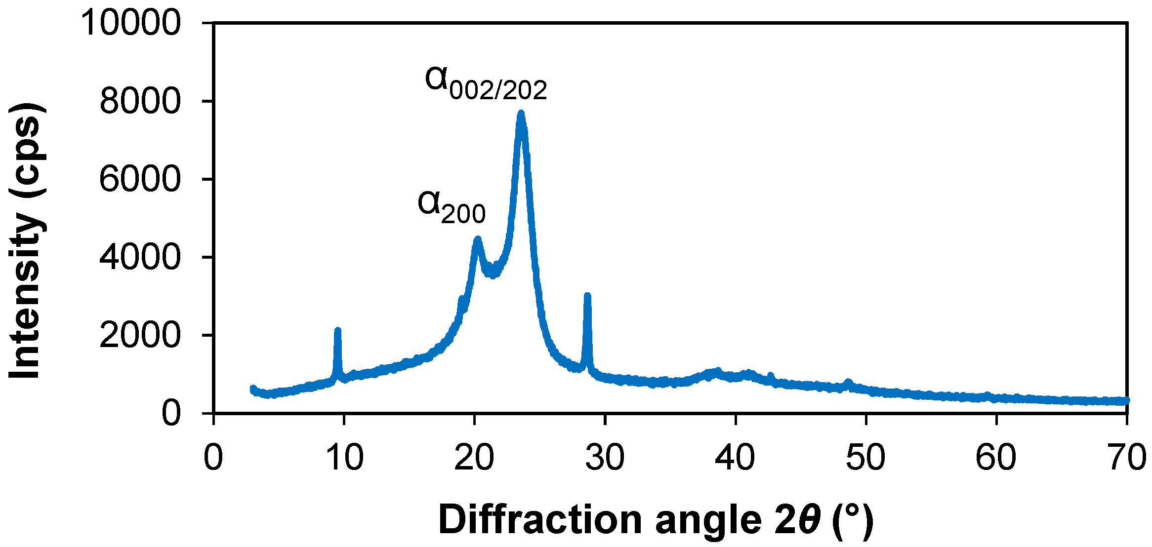
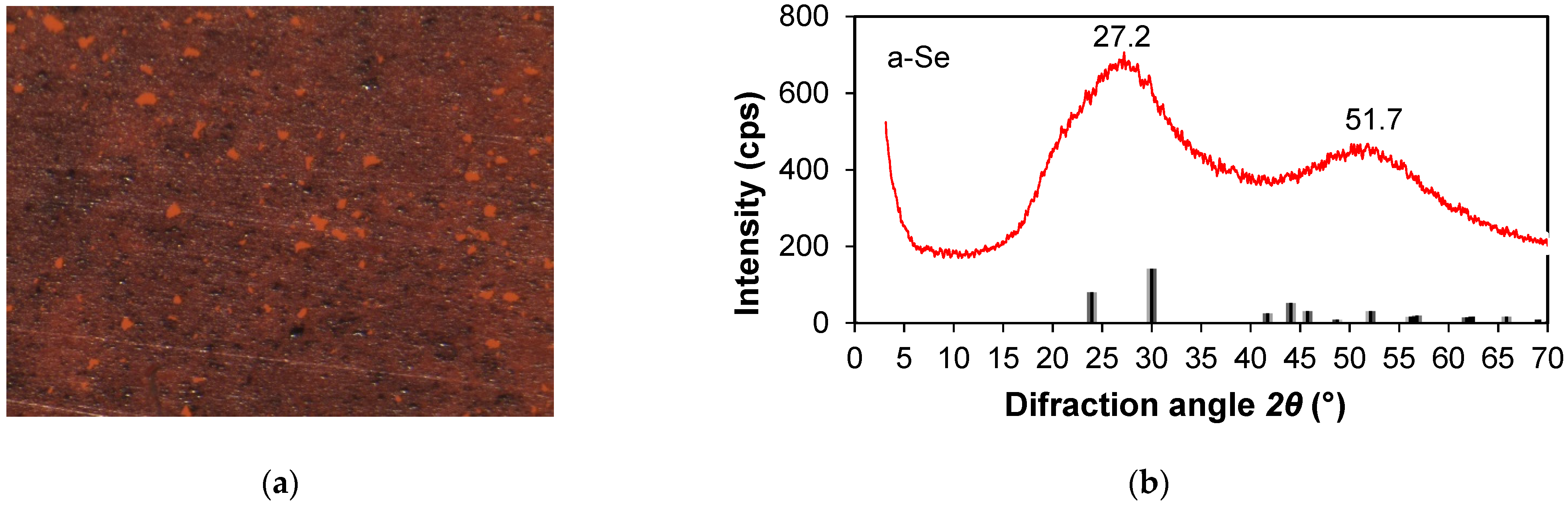
3.1. XRD Analysis
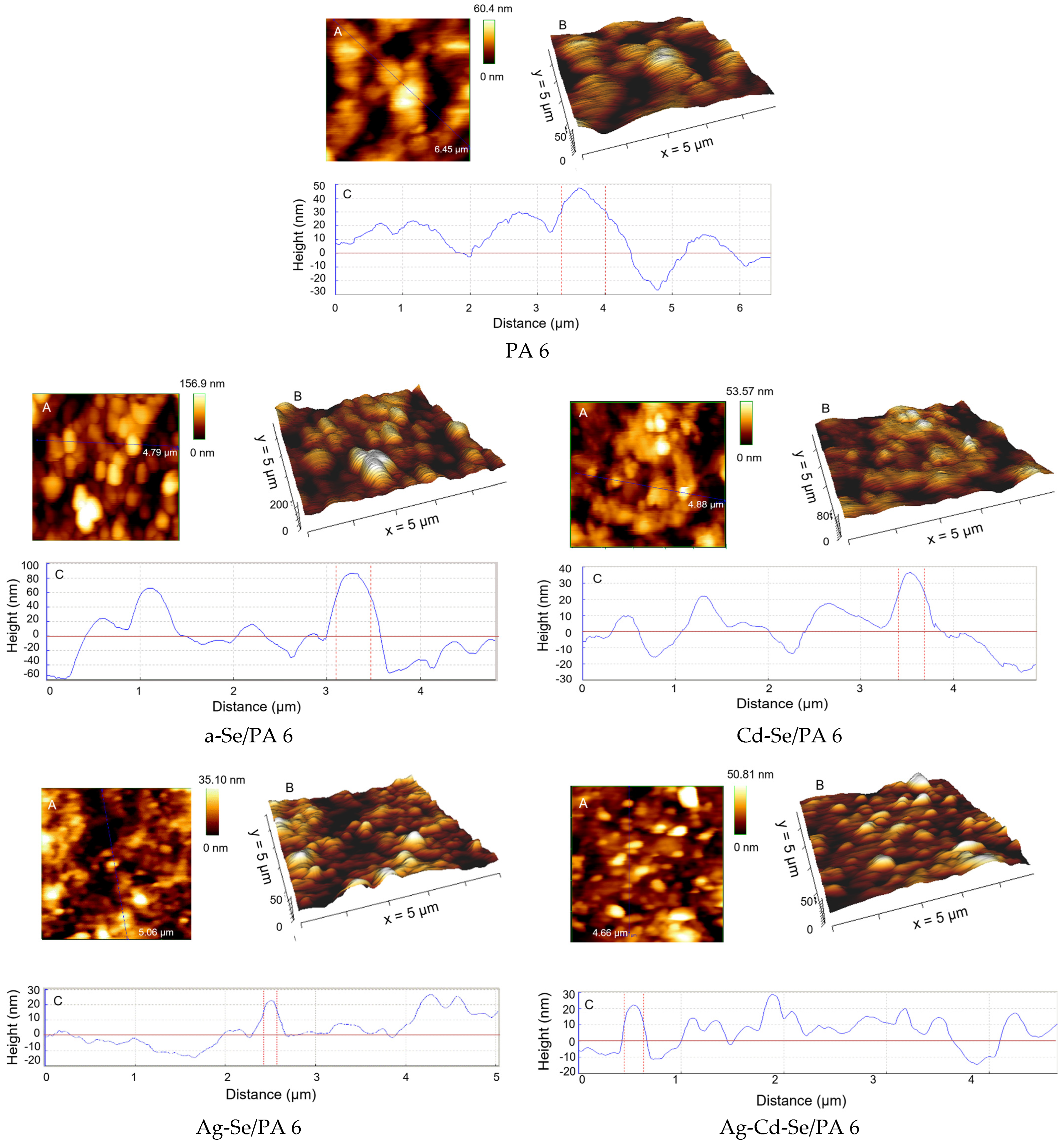
3.2. AFM Analysis
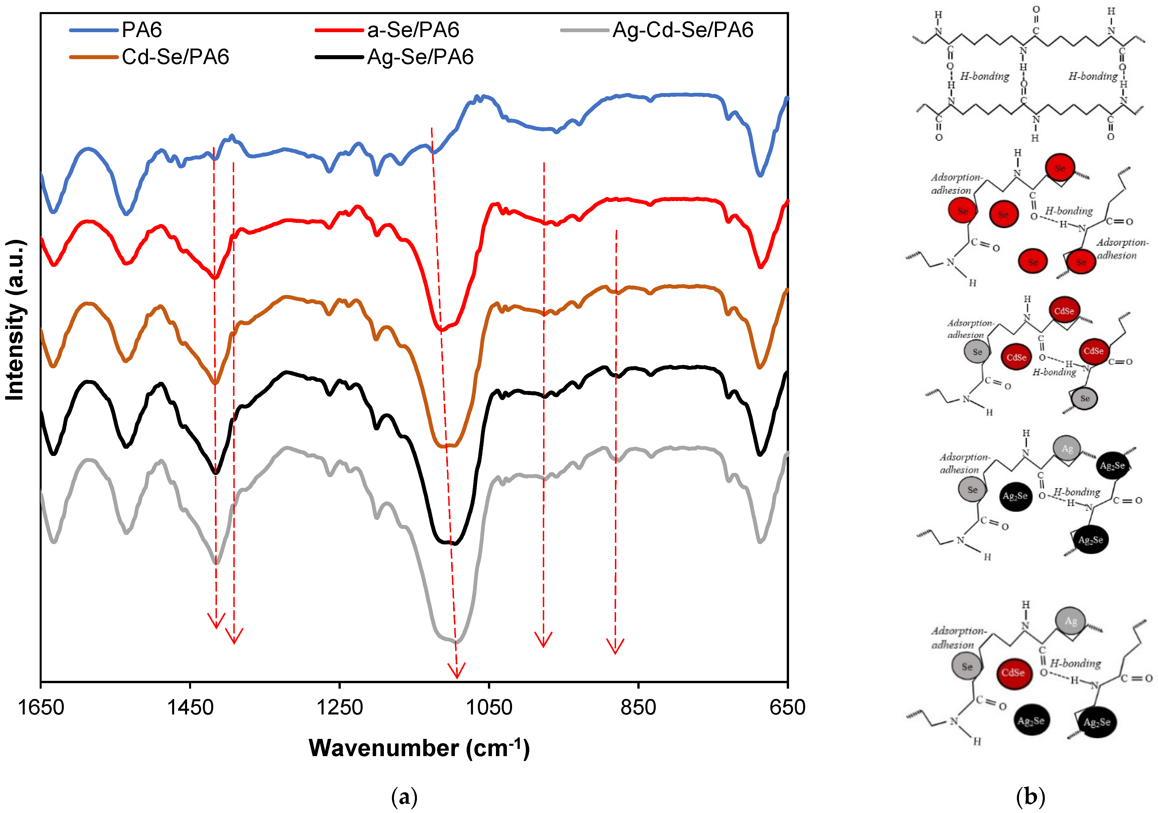
3.3. ATR-FTIR Analysis
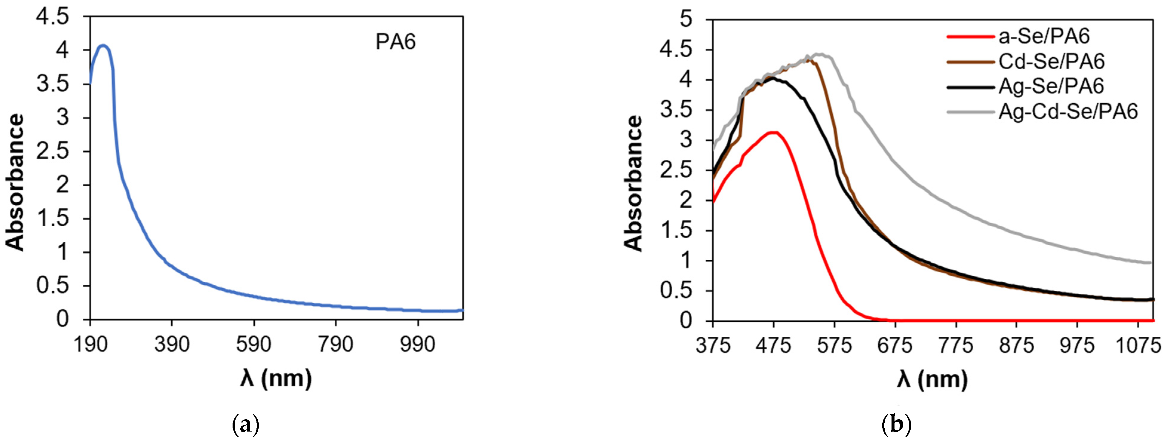
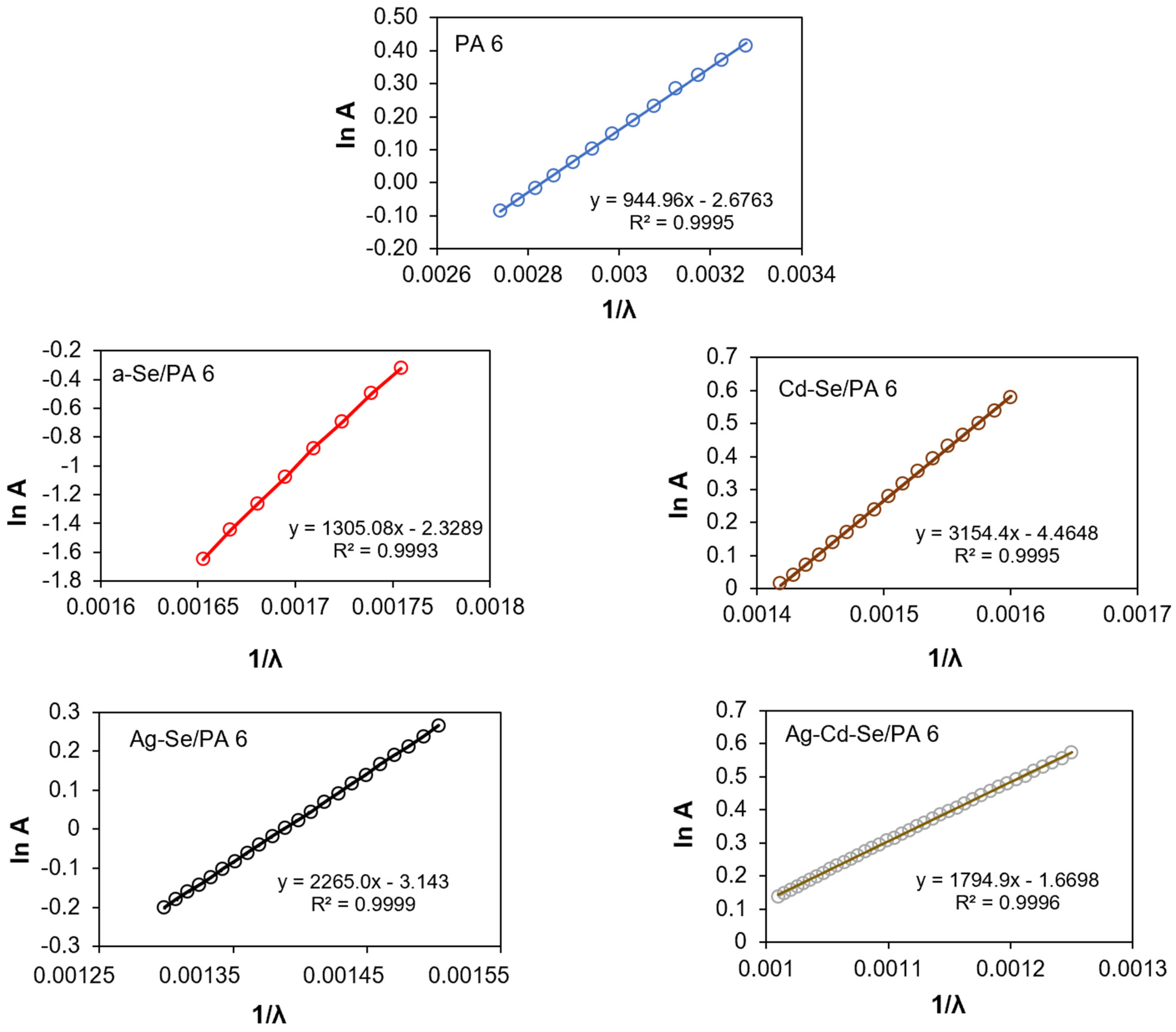
3.4. UV–Vis Analysis
4. Conclusions
Author Contributions
Funding
Institutional Review Board Statement
Informed Consent Statement
Data Availability Statement
Conflicts of Interest
References
- Park, Y.; Advincula, R.C. Hybrid semiconductor nanoparticles: π-conjugated ligands and nanostructured films. Chem. Mater. 2011, 23, 4273–4294. [Google Scholar] [CrossRef]
- Liu, R. Hybrid organic/inorganic nanocomposites for photovoltaic cells. Materials 2014, 7, 2747–2771. [Google Scholar] [CrossRef] [PubMed]
- Soler-Illia, G.J.; Azzaroni, O. Multifunctional hybrids by combining ordered mesoporous materials and macromolecular building blocks. Chem. Soc. Rev. 2011, 40, 1107–1150. [Google Scholar] [CrossRef] [PubMed]
- Willner, I.; Willner, B. Functional nanoparticle architectures for sensoric, optoelectronic, and bioelectronic applications. Pure Appl. Chem. 2002, 74, 1773–1783. [Google Scholar] [CrossRef]
- Di Luccio, T.; Piscopiello, E.; Laera, A.M.; Antisari, M.V. Structural studies of thin films of semiconducting nanoparticles in polymer matrices. Mater. Sci. Eng. C 2007, 27, 1372–1376. [Google Scholar] [CrossRef]
- Gates, B.; Mayers, B.; Cattle, B.; Xia, Y. Synthesis and characterization of uniform nanowires of trigonal selenium. Adv. Funct. Mater. 2002, 12, 219–227. [Google Scholar] [CrossRef]
- Jiang, F.; Cai, W.; Tan, G. Facile Synthesis and optical properties of small selenium nanocrystals and nanorods. Nanoscale Res. Lett. 2017, 12, 401. [Google Scholar] [CrossRef]
- Barik, A.R.; Adarsh, K.V.; Naik, R.; Ganesan, R.; Yang, G.; Zhao, D.; Jain, H.; Shimakawa, K. Role of rigidity and temperature in the kinetics of photodarkening in GexAs(45−x)Se55 thin films. Opt. Express 2011, 19, 13158–13163. [Google Scholar] [CrossRef]
- Udachan, S.; Ayachit, N.; Udachan, L.; Halembre, R. Impact of thickness on the optical properties of selenium thin films. Ing. Univ. 2020, 25, 1–24. [Google Scholar] [CrossRef]
- Lu, D.K.; Chang, Y.F.; Yang, H.Y.; Xie, F. Sequential removal of selenium and tellurium from copper anode slime with high nickel content. Trans. Nonferrous Met. Soc. China 2015, 25, 1307–1314. [Google Scholar] [CrossRef]
- Afzaal, M.; O’Brien, P. Recent developments in II–VI and III–VI semiconductors and their applications in solar cells. J. Mater. Chem. 2006, 16, 1597–1602. [Google Scholar] [CrossRef]
- Gao, Q.; Wang, W.; Lu, Y.; Cai, K.; Li, Y.; Wang, Z.; Wu, M.; Huang, C.; He, J. High power factor Ag/Ag2Se composite films for flexible thermoelectric generators. ACS Appl. Mater. Interfaces 2021, 13, 14327–14333. [Google Scholar] [CrossRef]
- Wu, M.; Cai, K.; Li, X.; Li, Y.; Liu, Y.; Lu, Y.; Wang, Z.; Zhao, W.; Wei, P. Ultraflexible and high-thermoelectric-performance sulfur-doped Ag2Se film on nylon for power generators. ACS Appl. Mater. Interfaces 2022, 14, 4307–4315. [Google Scholar] [CrossRef] [PubMed]
- Roy, S.; Tuinenga, C.; Fungura, F.; Dagtepe, P.; Chikan, V.; Jasinski, J. Progress toward producing n-type CdSe quantum dots: Tin and indium doped CdSe quantum dots. J. Phys. Chem. C 2009, 113, 13008–13015. [Google Scholar] [CrossRef]
- Liu, J.; Zhao, Q.; Liu, J.L.; Wu, Y.S.; Cheng, Y.; Ji, M.W.; Qian, M.H.; Hao, W.C.; Zhang, L.J.; Wei, X.J.; et al. Heterovalent-doping-enabled efficient dopant luminescence and controllable electronic impurity via a new strategy of preparing II–VI nanocrystals. Adv. Mater. 2015, 27, 2753–2761. [Google Scholar] [CrossRef] [PubMed]
- Wang, F.D.; Dong, A.G.; Buhro, W.E. Solution–liquid–solid synthesis, properties, and applications of one-dimensional colloidal semiconductor nanorods and nanowires. Chem. Rev. 2016, 116, 10888–10933. [Google Scholar] [CrossRef]
- Coughlan, C.; Ibanez, M.; Dobrozhan, O.; Singh, A.; Cabot, A.; Ryan, K.M. Compound copper chalcogenide nanocrystals. Chem. Rev. 2017, 117, 5865–6109. [Google Scholar] [CrossRef]
- Liu, J.; Zhang, J. Nanointerface chemistry: Lattice-mismatch-directed synthesis and application of hybrid nanocrystals. Chem. Rev. 2020, 120, 2123–2170. [Google Scholar] [CrossRef]
- Agranovich, V.M.; Gartstein, Y.N.; Litinskaya, M. Hybrid resonant organic–inorganic nanostructures for optoelectronic applications. Chem. Rev. 2011, 111, 5179–5214. [Google Scholar] [CrossRef]
- Mehta, C.; Abbas, J.M.; Saini, G.S.S.; Tripathi, S.K. Effect of deposition parameters on the optical and electrical properties of nanocrystalline CdSe. Chalcogenide Lett. 2007, 4, 133–138. [Google Scholar]
- Pejova, B.; Najdoski, M.; Grozdanov, I.; Dey, S.K. Chemical bath deposition of nanocrystalline (111) textured Ag2Se thin films. Mater. Lett. 2000, 43, 269–273. [Google Scholar] [CrossRef]
- Gates, B.; Yin, Y.; Xia, Y. A Solution-phase approach to the synthesis of uniform nanowires of crystalline selenium with lateral dimensions in the range of 10–30 nm. J. Am. Chem. Soc. 2000, 122, 12582–12583. [Google Scholar] [CrossRef]
- Lee, J.C.; Kurniawan, K.; Chung, K.W.; Kim, S. Metallurgical process for total recovery of all constituent metals from copper anode slimes: A review of established technologies and current progress. Met. Mater. Int. 2021, 27, 2160–2187. [Google Scholar] [CrossRef]
- Li, Z.; Huang, D.; McDonald, L.M. Heterogeneous selenite reduction by zero valent iron steel wool. Water Sci. Technol. 2017, 75, 908–915. [Google Scholar] [CrossRef]
- Liang, L.; Yang, W.; Guan, X.; Li, J.; Xu, Z.; Wu, J.; Huang, Y.; Zhang, X. Kinetics and mechanisms of pH-dependent selenite removal by zero valent iron. Water Res. 2013, 47, 5846–5855. [Google Scholar] [CrossRef]
- Liang, L.P.; Jiang, X.; Yang, W.J.; Huang, Y.Y.; Guan, X.H.; Li, L.N. Kinetics of selenite reduction by zero-valent iron. Desalin. Water Treat. 2015, 53, 2540–2548. [Google Scholar] [CrossRef]
- Jain, R.; Jordan, N.; Schild, D.; van Hullebusch, E.D.; Weiss, S.; Franzen, C.; Farges, F.; Hübner, R.; Lens, P.N.L. Adsorption of zinc by biogenic elemental selenium nanoparticles. Chem. Eng. J. 2015, 260, 855–863. [Google Scholar] [CrossRef]
- Baeshov, A.; Baeshova, A. A reduction phenomenon on the anode surface: Selenate and copper (II) ions reduction to their elemental state on the anode surface. J. Chem. Technol. Metall. 2020, 55, 1105–1110. [Google Scholar]
- Kalaparthi, R.; Korapu, S.; Gandam, H.; Kurimella, V.R. Synthesis of selenium nanoparticles using sodium selenite [Se(IV)] as a precursor and titanium(III) chloride as a reducing agent. Int. J. Eng. Res. 2020, 9, 359–363. [Google Scholar] [CrossRef]
- Geoffroy, N.; Demopoulos, G.P. Stannous chloride—An effective reducing agent for the removal of selenium(IV) from acidic solution. J. Chem. Technol. Biotechnol. 2012, 87, 983–989. [Google Scholar] [CrossRef]
- Geoffroy, N.; Demopoulos, G.P. Reductive precipitation of elemental selenium from selenious acidic solutions using sodium dithionite. Ind. Eng. Chem. Res. 2009, 48, 10240–10246. [Google Scholar] [CrossRef]
- Vieira, A.P.; Stein, E.M.; Andreguetti, D.X.; Cebrián-Torrejón, G.; Doménech-Carbó, A.; Colepicolod, P.; Ferreira, A.M.D.C. “Sweet Chemistry”: A green way for obtaining selenium nanoparticles active against cancer cells. J. Braz. Chem. Soc. 2017, 28, 2021–2027. [Google Scholar] [CrossRef]
- Vahdati, M.; Moghadam, T.T. Synthesis and characterization of selenium nanoparticles lysozyme nanohybrid system with synergistic antibacterial properties. Sci. Rep. 2020, 10, 510. [Google Scholar] [CrossRef] [PubMed]
- Kunita, M.H.; Girotto, E.M.; Radovanovic, E.; Gonçalves, M.C.; Ferreira, O.P.; Muniz, E.C.; Rubira, A.F. Deposition of copper sulfide on modified low-density polyethylene surface: Morphology and electrical characterization. Appl. Surf. Sci. 2002, 202, 223–231. [Google Scholar] [CrossRef]
- Essaidia, H.; Gantassi, A.; Touihria, S.; Ouerfelli, J. Tuning the structural, optical and electrical properties of AgInSe2 thin films prepared by sequentially deposited silver and indium nano-films under vacuum. Optik 2019, 182, 866–875. [Google Scholar] [CrossRef]
- Sutapa, I.W.; Wahab, A.W.; Taba, P.; Nafie, N.L. Dislocation, crystallite size distribution and lattice strain of magnesium oxide nanoparticles. J. Phys. Conf. Ser. 2018, 979, 012021. [Google Scholar] [CrossRef]
- Souri, D.; Tahan, Z.E. A new method for the determination of optical band gap and the nature of optical transitions in semiconductors. Appl. Phys. B Lasers Opt. 2015, 119, 273–279. [Google Scholar] [CrossRef]
- Souri, D.; Shomalian, K. Band gap determination by absorption spectrum fitting method (ASF) and structural properties of different compositions of (60 − x) V2O5–40TeO2–xSb2O3 glasses. J. Non Cryst. Solids 2009, 355, 1597–1601. [Google Scholar] [CrossRef]
- Solaymani, S.; Talu, S.; Nezafat, N.B.; Dejam, L.; Shafiekhani, A.; Ghaderi, A.; Zelati, A. Optical properties and surface dynamics analyses of homojunction and hetrojunction Q/ITO/ZnO/NZO and Q/ITO/ZnO/NiO thin films. Results Phys. 2021, 29, 104679. [Google Scholar] [CrossRef]
- Krylova, V. The study of silver sulfide layers formed on the polyamide film surface. Chemija 2012, 23, 203–209. [Google Scholar]
- Krylova, V.; Dukštienė, N.; Žalenkienė, S.; Baltrusaitis, J. Chemical and structural changes in polyamide based organic–inorganic hybrid materials upon incorporation of SeS2O62− precursor. Appl. Surf. Sci. 2017, 392, 634–641. [Google Scholar] [CrossRef]
- Zhao, Z.; Zheng, W.; Tian, H.; Yu, W.; Han, D.; Li, B. Crystallization behaviors of secondarily quenched Nylon 6. Mater. Lett. 2007, 61, 925–928. [Google Scholar] [CrossRef]
- Du, J.L.; Fang, Y.; Fu, E.G.; Ding, X.; Yu, K.Y.; Wang, Y.G.; Wang, Y.Q.; Baldwin, J.K.; Wang, P.P.; Bai, Q. What determines the interfacial configuration of Nb/Al2O3 and Nb/MgO interface. Sci. Rep. 2016, 6, 33931. [Google Scholar] [CrossRef] [PubMed]
- Park, S.H.; Choi, J.Y.; Lee, Y.H.; Park, J.T.; Song, H. Formation of metal selenide and metal-selenium nanoparticles using distinct reactivity between selenium and noble metals. Chem. Asian J. 2015, 10, 1452–1456. [Google Scholar] [CrossRef]
- Yanhui, Z.; Xu, M.; Liu, Y.; Bai, Y.; Deng, Y.; Liu, J.; Chen, L. Green synthesis of Se/Ru alloy nanoparticles using gallic acid and evaluation of their anti-invasive effects in HeLa cells. Colloids Surf. B 2016, 44, 118–124. [Google Scholar] [CrossRef]
- Olin, Å.; Noläng, B.; Osadchii, E.G.; Öhman, L.-O.; Rosén, E. Chemical Thermodynamics of Selenium, 1st ed.; Elsevier Science: Amsterdam, The Netherlands, 2005; 894p, Available online: https://www.oecd-nea.org/dbtdb/pubs/vol7-selenium.pdf (accessed on 16 August 2023).
- Jiang, X.; Mayers, B.; Herricks, T.; Xia, Y. Direct synthesis of Se@CdSe nanocables and CdSe nanotubes by reacting cadmium salts with Se nanowires. Adv. Mater. 2003, 15, 1740–1743. [Google Scholar] [CrossRef]
- Gates, B.; Mayers, B.; Wu, Y.; Sun, Y.; Cattle, B.; Yang, P.; Xia, Y. Synthesis and characterization of crystalline Ag2Se nanowires through a template-engaged reaction at room temperature. Adv. Funct. Mater. 2002, 12, 679–686. [Google Scholar] [CrossRef]
- Ayele, D.W. A facile one-pot synthesis and characterization of Ag2Se nanoparticles at low temperature. Egypt. J. Basic Appl. Sci. 2016, 3, 149–154. [Google Scholar] [CrossRef]
- Gates, B.; Wu, Y.; Yin, Y.; Yang, P.; Xia, Y. Single-crystalline nanowires of Ag2Se can be synthesized by templating against nanowires of trigonal Se. J. Am. Chem. Soc. 2001, 123, 11500–11501. [Google Scholar] [CrossRef]
- Jiang, Z.-Y.; Xie, Z.-X.; Zhang, X.-H.; Huang, R.-B.; Zheng, L.-S. Conversion of Se nanowires to Se/Ag2Se nanocables and Ag2Se nanotubes. Chem. Phys. Lett. 2003, 378, 313–316. [Google Scholar] [CrossRef]
- Kienle, L.; Duppel, V.; Mogwitz, B.; Janek, J.; Kreutzbruck, M.V.; Leineweber, A.; Simon, A. Synthesis–real structure–property: The showcase of silver-rich Ag2Se. Cryst. Growth Des. 2011, 11, 2412–2421. [Google Scholar] [CrossRef]
- Porter, D.A.; Easterling, K.E. Phase Transformations in Metals and Alloys, 4th ed.; CRC Press: Boca Raton, FL, USA, 2022. [Google Scholar]
- Luo, Y.R. Comprehensive Handbook of Chemical Bond Energies, 1st ed.; CRC Press: Boca Raton, FL, USA, 2007. [Google Scholar]
- Saruyama, M.; Sato, R.; Teranishi, T. Transformations of ionic nanocrystals via full and partial ion exchange reactions. Acc. Chem. Res. 2021, 54, 765–775. [Google Scholar] [CrossRef]
- Thiel, F.; Palencia, C.; Weller, H. Kinetic analysis of the cation exchange in nanorods from Cu2−xS to CuInS2: Influence of djurleite’s phase transition temperature on the mechanism. ACS Nano 2023, 17, 3676–3685. [Google Scholar] [CrossRef]
- Beberwyck, B.J.; Surendranath, Y.; Alivisatos, A.P. Cation exchange: A versatile tool for nanomaterials synthesis. J. Phys. Chem. C 2013, 117, 19759–19770. [Google Scholar] [CrossRef]
- Liu, G.; Liu, Y.; Zhao, J.; Pan, A.; Wang, B.; Zhu, T. Controllable Ag migration to form one-dimensional Ag/Ag2S@ZnS for bifunctional catalysis. ACS Appl. Energy Mater. 2020, 3, 6146–6154. [Google Scholar] [CrossRef]
- Stehlik, S.; Shimakawa, K.; Wagner, T.; Frumar, M. Diffusion of Ag ions under random potential barriers in silver-containing chalcogenide glasses. J. Phys. D Appl. Phys. 2012, 45, 205304. [Google Scholar] [CrossRef]
- Bhushan, B. Surface Roughness Analysis and Measurement Techniques; Modern Tribology Handbook; CRC Press LLC: Boca Raton, FL, USA, 2001; pp. 48–114. [Google Scholar]
- Gadelmawla, E.S.; Koura, M.M.; Maksoud, T.M.A.; Elewa, I.M.; Soliman, H.H. Roughness parameters. J. Mater. Process. Technol. 2002, 123, 133–145. [Google Scholar] [CrossRef]
- Song, G.; Wang, Y.; Tan, D.Q. A review of surface roughness impact on dielectric film properties. IET Nanodielectr. 2022, 5, 1–23. [Google Scholar] [CrossRef]
- He, X.; Liao, W.; Wang, G.; Zhong, L.; Li, M. Evaluation of hydrodynamic lubrication performance of textured surface from the perspective of skewness and kurtosis. Ind. Lubr. Tribol. 2018, 70, 829–837. [Google Scholar] [CrossRef]
- Caban, R.; Gnatowski, A. Structural and thermal examinations of polyamide modified with fly ash from biomass combustion. Materials 2023, 16, 5277. [Google Scholar] [CrossRef]
- Krylova, V.; Dukštienė, N. The structure of PA-Se-S-Cd composite materials probed with FTIR spectroscopy. Appl. Surf. Sci. 2019, 470, 462–471. [Google Scholar] [CrossRef]
- Sun, H.; Zhu, X.; Yang, D.; Wangyang, P.; Gao, X.; Tian, H. An economical method for amorphous selenium thick films preparation: E-beam evaporation. Mater. Lett. 2016, 183, 94–96. [Google Scholar] [CrossRef]
- Tüzüner, S.; Demir, M.M. Dispersion of organophilic Ag nanoparticles in PS-PMMA blends. Mater. Chem. Phys. 2015, 162, 692–699. [Google Scholar] [CrossRef]
- Ji, Y.; Yang, X.; Ji, Z.; Zhu, L.; Ma, N.; Chen, D.; Jia, X.; Tang, J.; Cao, Y. DFT-calculated IR spectrum amide I, II, and III band contributions of N-methylacetamide fine components. ACS Omega 2020, 5, 8572–8578. [Google Scholar] [CrossRef] [PubMed]
- Kotkata, M.F.; Masoud, A.E.; Mohamed, M.B.; Mahmoud, E.A. Structural characterization of chemically synthesized CdSe nanoparticles. Phys. E Low-Dimens. 2009, 41, 640–645. [Google Scholar] [CrossRef]
- Zeng, Y.; Kelley, D.F. Surface charging in CdSe quantum dots: Infrared and transient absorption spectroscopy. J. Phys. Chem. C 2017, 121, 16657–16664. [Google Scholar] [CrossRef]
- Qu, J.; Goubet, N.; Livache, C.; Martinez, B.; Amelot, D.; Gréboval, C.; Chu, A.; Ramade, J.; Cruguel, H.; Ithurria, S.; et al. Intraband mid-Infrared transitions in Ag2Se nanocrystals: Potential and limitations for Hg free low cost photodetection. J. Phys. Chem. C 2018, 122, 18161–18167. [Google Scholar] [CrossRef]
- Sadtler, B.; Demchenko, D.O.; Zheng, H.; Hughes, S.M.; Merkle, M.G.; Dahmen, U.; Wang, L.-W.; Alivisatos, A.P. Selective facet reactivity during cation exchange in cadmium sulfide nanorods. J. Am. Chem. Soc. 2009, 131, 5285–5293. [Google Scholar] [CrossRef]
- Lin, Z.H.; Wang, C.R.C. Evidence on the size-dependent absorption spectral evolution of selenium nanoparticles. Mater. Chem. Phys. 2005, 92, 591–594. [Google Scholar] [CrossRef]
- Panahi-Kalamuei, M.; Mousavi-Kamazani, M.; Salavati-Niasari, M.; Mostafa Hosseinpour-Mashkani, S. A simple sonochemical approach for synthesis of selenium nanostructures and investigation of its light harvesting application. Ultrason. Sonochem. 2015, 23, 246–256. [Google Scholar] [CrossRef]
- Surana, K.; Salisu, I.T.; Mehra, R.M.; Bhattacharya, B. A simple synthesis route of low temperature CdSe-CdS core-shell quantum dots and its application in solar cell. Opt. Mater. 2018, 82, 135–140. [Google Scholar] [CrossRef]
- Hegazy, M.A.; Abd El-Hameed, A.M. Characterization of CdSe-nanocrystals used in semiconductors for aerospace applications: Production and optical properties. NRIAG J. Astron. Geophys. 2014, 3, 82–87. [Google Scholar] [CrossRef]
- Ramezanloo, B.; Molaei, M.; Karimipour, M. Red emissive Ag2Se quantum dots (QDs) with room-temperature synthesis of both orthorhombic and superionic cubic phases via stirring approach. J. Lumin. 2018, 204, 419–423. [Google Scholar] [CrossRef]
- Singh, S.; Bharti, A.; Meena, V.K. Green synthesis of multi-shaped silver nanoparticles: Optical, morphological and antibacterial properties. J. Mater. Sci. Mater. Electron. 2015, 26, 3638–3648. [Google Scholar] [CrossRef]
- Xu, X.; Wang, X.; Zhang, Y.; Li, P. Ion-exchange synthesis and improved photovoltaic performance of CdS/Ag2S heterostructures for inorganic-organic hybrid solar cells. Solid State Sci. 2016, 61, 195–200. [Google Scholar] [CrossRef]
- Di, T.; Cheng, B.; Ho, W.; Yu, J.; Tang, H. Hierarchically CdS–Ag2S nanocomposites for efficient photocatalytic H2 production. Appl. Surf. Sci. 2019, 470, 196–204. [Google Scholar] [CrossRef]
- Bubenov, S.S.; Dorofeev, S.G.; Kotin, P.A.; Znamenkov, K.O.; Kuznetsova, T.A. Oleic capped CdSe nanocrystals silver doped in the course of synthesis. Mendeleev Commun. 2014, 24, 250–252. [Google Scholar] [CrossRef]
- Asadpour-Zeynali, K.; Mollarasouli, F. A novel and facile synthesis of TGA-capped CdSe@Ag2Se core-shell quantum dots as a new substrate for high sensitive and selective methyldopa sensor. Sens. Actuator B Chem. 2016, 237, 387–399. [Google Scholar] [CrossRef]
- Ansari, M.Z.; Khare, N. Effect of intrinsic strain on the optical band gap of single phase nanostructured Cu2ZnSnS4. Mater. Sci. Semicond. Process 2017, 63, 220–226. [Google Scholar] [CrossRef]
- Purushotham, E.; Krishna, N.G. Effect of particle size and lattice strain on Debye-Waller factors of Fe3C nanoparticles. Bull. Mater. Sci. 2014, 37, 773–778. [Google Scholar] [CrossRef]
- Li, J.; Zhu, X.; Yang, D.; Gu, P.; Wu, H. Investigations on structural, optical and X-radiation responsive properties of a-Se thin films fabricated by thermal evaporation method at low vacuum degree. Materials 2018, 11, 368. [Google Scholar] [CrossRef] [PubMed]
- Shportko, K.V. Disorder and compositional dependences in Urbach-Martienssen tails in amorphous (GeTe)x(Sb2Te3)1−x alloys. Sci. Rep. 2019, 9, 6030. [Google Scholar] [CrossRef] [PubMed]
- Kaiser, C.; Sandberg, O.J.; Zarrabi, N.; Li, W.; Meredith, P.; Armin, A. A universal Urbach rule for disordered organic semiconductors. Nat. Commun. 2021, 12, 3988. [Google Scholar] [CrossRef] [PubMed]
- Zhang, C.J.; Mahadevan, S.; Yuan, J.; Ho, J.K.W.; Gao, Y.X.; Liu, W.; Zhong, H.; Yan, H.; Zou, Y.P.; Tsang, S.W.; et al. Unraveling Urbach tail effects in high performance organic photovoltaics: Dynamic vs static disorder. ACS Energy Lett. 2022, 7, 1971–1979. [Google Scholar] [CrossRef]
- Ambrosone, G.; Basa, D.K.; Coscia, U.; Fathallah, M. Study on the microstructural and overall disorder in hydrogenated amorphous silicon carbon films. J. Appl. Phys. 2008, 104, 123520. [Google Scholar] [CrossRef]
- Rani, S.; Sanghi, S.; Agarwal, A.; Seth, V.P. Study of optical band gap and FTIR spectroscopy of Li2O·Bi2O3·P2O5 glasses. Spectrochim. Acta A 2009, 74, 673–677. [Google Scholar] [CrossRef]
- Ananth Kumar, R.T.; Chithra Lekha, P.; Sanjeeviraja, C.; Pathinettam Padiyan, D. Evolution of structural disorder using Raman spectra and Urbach energy in GeSe0.5S1.5 thin films. J. Non-Cryst. 2014, 405, 21–26. [Google Scholar] [CrossRef]
- Kabir, H.; Rahman, M.M.; Uddin, K.M.; Bhuiyand, A.H. Structural, morphological, compositional and optical studies of plasma polymerized 2-furaldehyde amorphous thin films. Appl. Surf. Sci. 2017, 423, 983–994. [Google Scholar] [CrossRef]


| Sample | Phase | 2θ, ° | Dc, nm | δ × 1015, m−2 | ε × 10−3 |
|---|---|---|---|---|---|
| PA 6 | PA6 | 23.5 | 16 | 3.70 | 2.11 |
| a-Se/PA 6 | PA6 | 23.7 | 17 | 3.33 | 2.00 |
| a-Se | – | – | – | – | |
| Cd-Se/PA 6 | PA6 | 23.5 | 17 | 3.38 | 2.01 |
| Se8 | 33.5 | 33 | 0.89 | 1.04 | |
| CdSe | 42.7 | 40 | 0.63 | 0.87 | |
| Ag-Se/PA 6 | PA6 | 23.6 | 17 | 3.56 | 2.06 |
| Se8 | 31.8 | 31 | 0.91 | 1.07 | |
| Ag2Se | 33.8 | 34 | 0.85 | 0.98 | |
| Ag | 43.4 | 34 | 0.89 | 1.02 | |
| Ag-Cd-Se/PA 6 | PA6 | 23.7 | 17 | 3.58 | 2.08 |
| Se8 | 31.8 | 30 | 1.10 | 1.15 | |
| CdSe | 48.7 | 37 | 0.74 | 0.94 | |
| Ag2Se | 33.6 | 35 | 0.84 | 1.00 | |
| Ag | 43.5 | 34 | 0.88 | 1.03 |
| Phase or Ion | G, kJ/mol | BDE, kJ/mol | KSP, (mol/dm3)n * | S, mol/dm3 |
|---|---|---|---|---|
| a-Se | 6.00 ± 2.2 | - | - | 2.2 × 10⁻⁸ |
| cr-Se | 0.00 | 332.6 (Se-Se) | - | 1.5 × 10⁻⁹ |
| Ag+ | 77.11 | - | - | - |
| Cd2+ | −77.16 | - | - | - |
| CdSe | −141.60 | 127.6 ± 25.1 | 1.0 × 10⁻³³ | 3.16 × 10⁻¹⁷ |
| Ag2Se | −46.90 | 210.0 ± 14.6 | 3.1 × 10−65 | 3.14 × 10⁻²² |
| Composite | Ra (nm) | RMS (nm) | Rt (nm) |
|---|---|---|---|
| PA 6 | 10.78 | 13.73 | 73.82 |
| a-Se/PA 6 | 27.61 | 35.66 | 145.30 |
| Cd-Se/PA 6 | 9.82 | 12.17 | 61.81 |
| Ag-Se/PA 6 | 7.93 | 10.17 | 41.32 |
| Ag-Cd-Se/PA 6 | 8.36 | 11.55 | 43.10 |
| Band Location, cm−1 | Assignment | ||||
|---|---|---|---|---|---|
| PA6 | a-Se/PA6 | Cd-Se/PA6 | Ag-Se/PA6 | Ag-Cd-Se/PA6 | |
| 687 | 687 | 687 | 687 | 687 | C–C bending |
| 730 | 730 | 729 | 730 | 729 | CH2 waging |
| 834 | 835 | 833 | 833 | 833 | CO–NH in plane |
| – | – | 877 | 877 | 876 | CdSe or/and Ag2Se |
| 929 | 929 | 930 | 930 | 930 | CO–NH in plane |
| 960 | 959 | 961 | 960 | 960 | CO–NH in plane (α crystalline) |
| – | 974 | 976 | 975 | 975 | |
| 1023 | 1023 | 1025 | 1024 | 1024 | trans C–C backbone conformation |
| 1031 | 1031 | 1031 | 1032 | 1031 | CO–NH in plane (α crystalline) |
| 1124 | 1112 | 1112 | 1108 | 1094 | C–C stretching (sym) |
| 1169 | 1165 | 1166 | 1166 | 1165 | N–C–O groups/CH2 twisting |
| 1200 | 1200 | 1200 | 1200 | 1201 | C–CH bending (sym) CH2 twisting |
| 1238 | 1238 | 1236 | 1237 | 1235 | |
| 1264 | 1264 | 1261 | 1263 | 1263 | C–N stretching (amide III) |
| 1365 | 1371 | 1376 | 1377 | 1377 | CH2 twisting |
| – | 1390 | 1392 | 1392 | 1391 | C–C stretching (sym) |
| 1417 | 1417 | 1417 | 1416 | 1415 | CH2 scissoring next to >C=O group |
| 1463 | 1459 | 1460 | 1459 | 1459 | CH2 scissoring |
| 1476 | 1475 | 1476 | 1475 | 1475 | CH2 scissoring next to N–H group |
| 1535 | 1534 | 1536 | 1536 | 1535 | C–N stretching and N–H bending of hydrogen-bonded N–H groups (amide II) |
| 1633 | 1633 | 1633 | 1633 | 1632 | C=O stretching (amide I) |
| Composite | λg, nm | Eg, eV | EU, eV | σ | Ee-p, eV | χ |
|---|---|---|---|---|---|---|
| PA 6 | 278 | 4.46± 0.02 | 1.31 | 0.020 | 33.33 | 1.20 |
| a-Se/PA 6 | 556 | 2.23± 0.02 | 0.95 | 0.027 | 24.69 | 0.60 |
| Cd-Se/PA 6 | 605 | 2.05± 0.02 | 0.39 | 0.066 | 10.10 | 0.55 |
| Ag-Se/PA 6 | 625 | 1.98± 0.02 | 0.55 | 0.047 | 14.18 | 0.53 |
| Ag-Cd-Se/PA 6 | 756 | 1.64± 0.02 | 0.69 | 0.037 | 18.02 | 0.44 |
Disclaimer/Publisher’s Note: The statements, opinions and data contained in all publications are solely those of the individual author(s) and contributor(s) and not of MDPI and/or the editor(s). MDPI and/or the editor(s) disclaim responsibility for any injury to people or property resulting from any ideas, methods, instructions or products referred to in the content. |
© 2023 by the authors. Licensee MDPI, Basel, Switzerland. This article is an open access article distributed under the terms and conditions of the Creative Commons Attribution (CC BY) license (https://creativecommons.org/licenses/by/4.0/).
Share and Cite
Skuodaitė, E.; Krylova, V. Synthesis and Characterization of Amorphous Selenium, Cadmium and Silver Selenide Thin Films on Polyamide-6. Coatings 2023, 13, 1661. https://doi.org/10.3390/coatings13101661
Skuodaitė E, Krylova V. Synthesis and Characterization of Amorphous Selenium, Cadmium and Silver Selenide Thin Films on Polyamide-6. Coatings. 2023; 13(10):1661. https://doi.org/10.3390/coatings13101661
Chicago/Turabian StyleSkuodaitė, Emilija, and Valentina Krylova. 2023. "Synthesis and Characterization of Amorphous Selenium, Cadmium and Silver Selenide Thin Films on Polyamide-6" Coatings 13, no. 10: 1661. https://doi.org/10.3390/coatings13101661