Article

Effects of Bias Voltage and Target Current on Microstructure and Load Measurement Performance of ZnO Piezoelectric Coatings Applied to Bolt in Transformer

1
State Grid East Inner Mongolia Electric Power Company, Hulunbeier 021000, China
2
Wuhan NARI Limited Liability Company of State Grid Power Research Institute, Wuhan 430010, China
*
Author to whom correspondence should be addressed.
Coatings 2023, 13(10), 1662; https://doi.org/10.3390/coatings13101662
Submission received: 14 August 2023 / Revised: 1 September 2023 / Accepted: 6 September 2023 / Published: 22 September 2023
(This article belongs to the Special Issue Surface Coatings and Technology Against Soil Abrasion and Adhesion)

Abstract

:
Electrical accidents caused by bolt looseness in transformers have been frequently reported in recent years. The monitoring, and warning of, axial force as an indicator of looseness is one of the key issues affecting the operation and maintenance of transformers. Traditional ultrasonic testing and a patch-type ultrasonic method, using piezoelectric probes and coupling agents, showed poor repeatability and accuracy in detecting the bolt pre-tightening force, because of the uncertainty of the contact interface produced via manual operation. A permanent thin-film pressure sensor (PMTS), which provides accurate and in-situ stress detection, is more suitable for bolts, to reveal the pretightening force. The key is depositing a nano-zinc oxide (ZnO) piezoelectric film with an excellent measurement performance, which could be tuned using deposition parameters. This paper investigates the effects of the current and bias voltage on the crystal structure and performance of ZnO piezoelectric films. The results show that the crystallinity degree and resistance decrease with the increase in bias voltage, while the target current could increase the crystallinity. However, a high current also brings large particles in the coating surface, which greatly decrease the resistance. The cause is expected to be related to the ion energy, which could be affected by the bias voltage and current. The PMTS deposited with an optimized bias voltage and current revealed excellent measurement performance, and is expected to be applied to the bolt, to detect the pretightening force.

1. Introduction

High-voltage bushing is the core component of the insulated lead in high-voltage transformers, and greatly affects safety and reliable operation. The bushings are always subjected to complex service environments, such as high-voltage electric fields, mechanical stress, and high–low temperature impacts, which lead to high risk for the structural components. The loosening of the bolt is one of the important failures which could lead to a severe electrical accident. The monitoring of the causes of high-voltage bushing accidents is one of the key aspects of digitizing high-voltage substations, and promoting the application of artificial intelligence in substations. Its core lies in the development of monitoring sensors. Currently, the safety monitoring of high-voltage bushing power systems, at home and abroad, mainly focuses on partial discharge, insulation systems, SF6 gas composition, dielectric loss, and other aspects [1,2]. Monitoring the cause and initial phenomenon of accidents is a vital element in digital substations cutting down accident rates. Currently, the safety monitoring of high-voltage bushing power systems mainly focuses on partial discharge, insulation systems, SF6 gas composition, and dielectric loss [3,4].
Rosolem et al. monitored the partial discharge in high-voltage bushings with optical fiber sensors [5]. Senobari R K reviewed the frequency response analysis method (FRA), based on the principle of dielectric response, to conduct insulation detection on bushings [6]. Cristaldi L explored the feasibility of online monitoring technology for dielectric loss in high-voltage bushings, from theory to equipment [7]. Sensors such as thin palladium film have been used in transformer oil, and have successfully detected the hydrogen gas dissolved [8]. The stress evolution in the connecting structure is an important cause of the above accident phenomenon. Several accidents, including a line trip, occurred in a 1000 KV UHV substation transformer in Central China [9], a burst accident occurred in a 500 KV substation in Anhui Province [10], and a heating failure in a 800 KV converter station was reported in Zhejiang Province, China, related to the seal failure induced via the connection loosening [11]. The reason was attributed to bolt looseness induced via the complex load among the connecting structure components, based on the subsequent investigation. However, the stress monitoring of the bolt is scarce, leading to the research gap in connecting mechanical failure and electrical accident. Currently, optical fiber, pressure thermoluminescence, strain gauge, ultrasonic methods, and guided wave methods are commonly used in detecting bolt stress. Ultrasonic testing technology is the most commonly used technology, because of its non-destructive characteristics.
Traditional ultrasonic testing needs to fill the interface with a coupling agent, to act against the acoustic impedance, to accept the reflected signal. The testing accuracy depends on the accurate measurement of the relationship between the acoustics and time, which could be greatly affected by the coupling layer. Thus, the poor precision of a coupling layer applied by hand determines the poor accuracy of traditional ultrasonic testing. In order to avoid the influence of coupling agents, the piezoelectric patch methods, which mainly uses polymer piezoelectric ceramic sheets attached to the surface of the work piece being tested, was developed. However, the detection accuracy is also affected by the adhesion layer. A permanent thin-film pressure sensor (PMTS) made from ZnO piezoelectric thin films, which could be directly deposited on the surface of the tested components, without the need for coupling agents and adhesive layers, presents a high accuracy and a strong anti-interference ability [12,13] in detecting stress. Meanwhile, the PMTS is conducive to achieving integrated design and manufacturing based on structure/perception [14]. The ZnO film is deposited via a sputtering method with a low deposition rate, which greatly limits its industrial application. The development of a deposition technology, and the optimization of the deposition process for film deposition, are urgent and significant issues in the development of a smart bolt to construct a digital transformer.
Arc ion plating, using arc discharge to evaporate materials, offers a high ionization rate, and excellent adhesion and mechanical properties. It has been used in the field of vacuum coating [15]. Aiming to combat the shortcomings of low production efficiency, and poor process repeatability and uniformity, in ZnO thin-film sputtering technology [16,17], arc ion plating was employed in this paper to deposited nano ZnO on an alloyed steel substrate. In this study, the effects of the target current and bias voltage on the crystal structure and performance of ZnO piezoelectric thin films were systematically explored, to optimize the process. Finally, a high-resistance and c-axis-preferred-orientation ZnO piezoelectric sensing coating material was prepared on the end face of a high-voltage bushing bolt, using the optimization process. The axial load and measured load of the bolt were calibrated using an ultrasonic system. The results provide a foundation for on-site bolt stress monitoring engineering applications.

2. Experimental Details

2.1. Coating Preparation

The coatings were deposited with a Zn target with a purity of 99.99% (provided by Guangdong Jushitai Powder Limited Company, Qingyuan, China). The ZnO coatings were deposited on mirror-polished Si (100)substrates (for SEM analysis), and a stainless steel substrate (for XRD measurement and resistance testing) with a size of 3 × 4 × 0.5 mm3, via a cathodic arc ion plating system (made by Weilide Vacuum Technology Company, Shenyang, China). The size of the chamber was 800 × 800 × 800 mm3, and the minimum distance between the samples and source was 225 mm. All substrates were cleaned using ultrasonic cleaner with acetone and alcohol for 10 min. Prior to deposition, Ar +ion bombardment was carried out, to remove contamination on the substrate surface, using an Ar2 (99.999%) atmosphere fixed at 6 × 10⁻³ Pa for 30 min. Then, the ZnO coatings were deposited in pure O2 with a pressure of 1.5 Pa. The bias voltages were set from 0 to 50, and to 100 V, with a current of 50 A. The target currents were set at 30, 40, and 50 A, with an affixed bias voltage of 0 V. All coatings were deposited for 1 h.

2.2. Microstructure and Resistance Test

The surface morphologies of the as-deposited coatings were observed via an FEI Sirion IMP SEM system, using samples. Semi-quantitative compositional analysis of the coatings was carried out, using energy-dispersive spectrometer analysis. X-ray diffraction (Bruker AXS D8 with a Cu K α radiation –λK α = 0.15418 nm) was used to obtain the phase structure of the as-deposited coatings. Cross-sectional analysis verification was performed via HRTEM (JEOL JEM 2010). The resistance was tested using a multimeter (made by Deli Group, Ningbo, China) with a measuring range from 200 Ω to 200 MΩ, and an accuracy of 0.3%.

2.3. Performance Testing of the Bolt with Coating Deposited via Optimized Process

A transformer bolt with a ZnO piezoelectric sensing coating at the end face was synthesized for the performance verification test (as shown in Figure 1a,b). The test was conducted in am HCL-3MC bolt-test machine, fixed as shown in Figure 1c. The force was set from 0 to 64 kN, and loaded with a gradient of 4 kN at room temperature. During the loading process, ultrasonic testing systems (JSR, DPR300) were used to measure the ultrasonic flight time at the bolt ends. The load and measured sound velocity were calibrated based on the principle of acoustic elasticity.

3. Results and Discussion

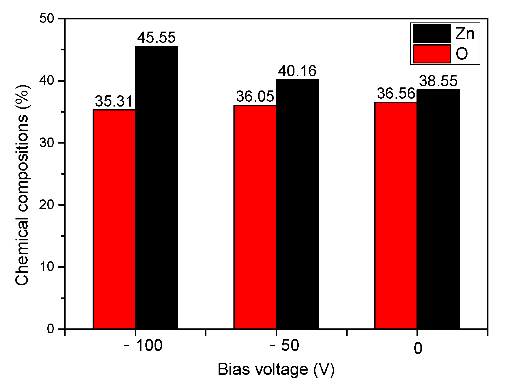
3.1. Effects of Bias Voltage on the Morphology and Growth Rate of ZnO Film

Figure 2 shows the surface and cross-sectional morphologies of ZnO coatings prepared under different bias voltages. Figure 1a–c were deposited with the bias voltages of 0 V, −50 V, and −100 V, respectively. From Figure 2, it can be seen that the surface morphology of the ZnO coatings all revealed a concave–convex structure as the bias voltage increased from 0 V to −50 V. This is a typical feature of arc-grown ZnO materials. However, when the bias voltage reached −100 V, many large particles were obtained on the coating surface, as shown in Figure 2c. The emergence of particles indicated that increasing the bias voltage would increase the number of large particle deposition defects on the surface. Through the analysis of the composition of large particles on the surface, it was found that the oxygen content of large particles was extremely low, and most of them were pure metal Zn directly ejected from the target material. This was a result of the accelerated movement of Zn particles, which derived from the high bias voltage, leading to there being little time for Zn particles to react with O before they reached the substrate.
Figure 2d–f show the cross-sectional morphologies of the coating under different bias voltages. It can be seen that all the coatings had a columnar crystal structure, perpendicular to the substrate. The columnar crystals became smaller as the bias voltage increased, resulting in a dense coating. Simultaneously, the thickness changed from 1.35 μm to 3.54 μm, and to 2.69 μm, as the bias voltage increased from 0 to 50, and to 100 V. This indicated that the deposition rate first increased and then decreased with the bias voltage. This is due to the fact that the bias voltage provides an accelerating electric field, which can effectively increase the speed at which Zn particles reach the substrate, thereby increasing the deposition rate. However, a 100 V bias voltage led to higher energy in the Zn particles, inducing a bombardment effect, through which many particles would be dropped from the substrate. Thus, coatings deposited at 100 V revealed a lower deposition rate.
The chemical compositions of ZnO coatings deposited with different bias voltages are shown in Figure 3. The content of Zn and O in the coating varied greatly with the bias voltage. Increasing the bias voltage led to a continuous increase in Zn, and decrease in O. This suggests that the oxygen vacancy defects and zinc gap atom defects increased. The reason was also related to the accelerated zinc ions that did not have sufficient time to react with O before reaching the substrate. Then, they would be covered by the subsequent-deposited atomic layer, ultimately obtaining a coating with a severely unbalanced chemical ratio, through cumulative benefits.

3.2. Effects of Bias Voltage on Crystal Characteristics and Resistance of Zno Coatings

Figure 4 showed the structural test results of ZnO coatings under different bias voltages. From the XRD results in Figure 3, it can be seen that the bias voltage has a significant impact on the growth orientation of the coating. The coatings revealed preferred-orientation (002) growth at low bias voltages, including 0 and 50 V, and then changed to several orientations as the bias voltage increased to 100 V. Apart from the evolution of the grain orientation, the angle of (002) also shifted to a higher angle because of residual stress induced by ion bombardment. The shifting angle increased with the bias voltage. The full width at half maximum (FWHM) and intensity of (002) orientation are further analyzed in Table 1. As the bias voltage increased, the diffraction peak intensity gradually decreased, while the FWHM value gradually increased, indicating that the crystalline quality of the coating gradually decreased. The surface energy of (002) is lowest. Thus, energetic ions, with the surface energy and diffusion time, would tend to migrate to this orientation. However, for ions generated under 100 V, the migration time decreased, and these ions would be limited to locations where they reached the surface. Thus, the coating exhibited a trend of multi-orientated growth. Therefore, increasing the bias voltage was not beneficial to achieving (002) preferred orientation. The resistance of coatings was tested, and the results are listed in Table 1. As the bias voltage increased, the resistance of the coating gradually decreased. It could be concluded that oxygen vacancy and metal particles were detrimental to the resistance, which could be an indicator of the piezoelectric property. Efforts should be made to achieve a low particle density and preferred (002) orientation [18,19].

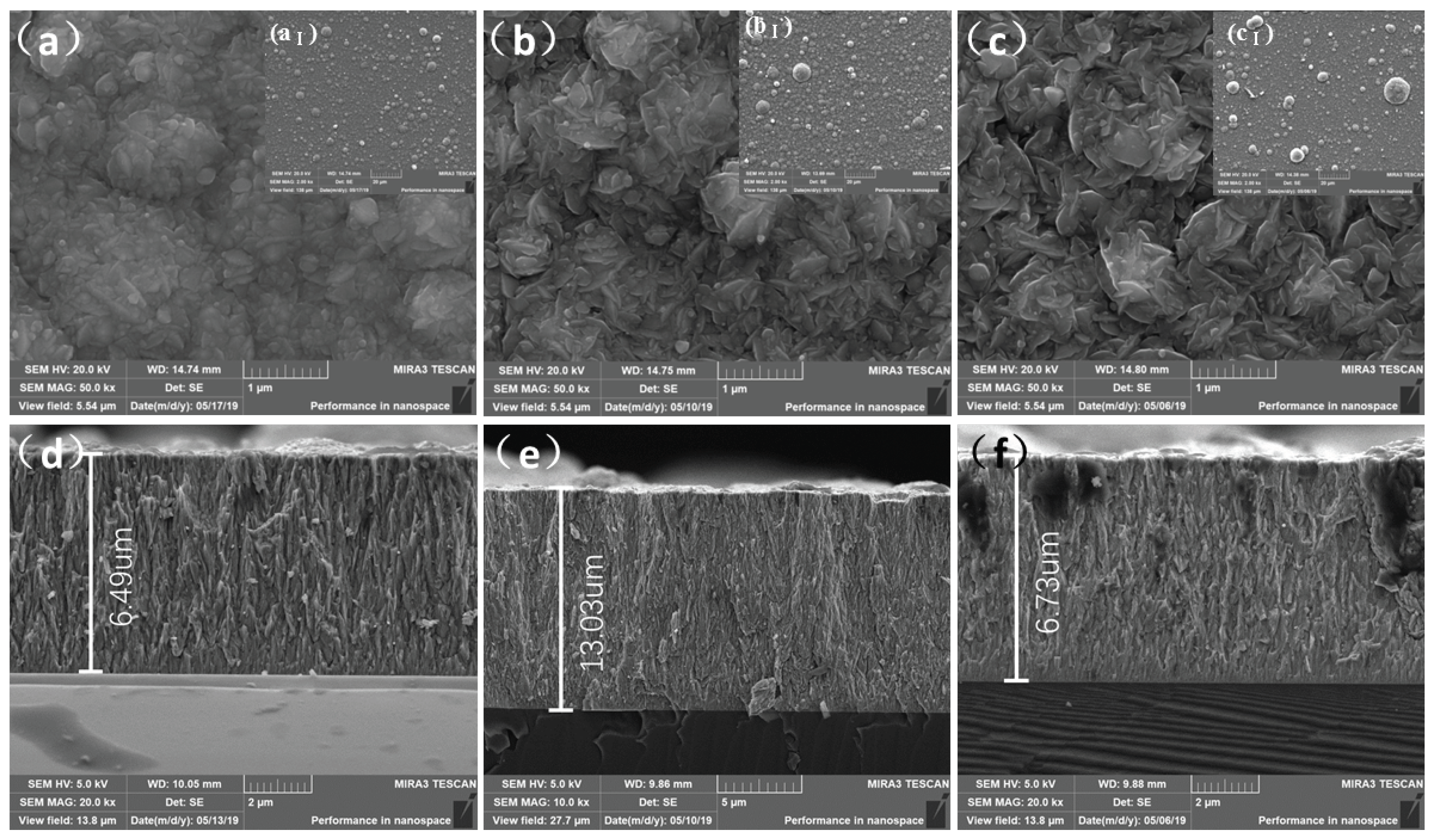
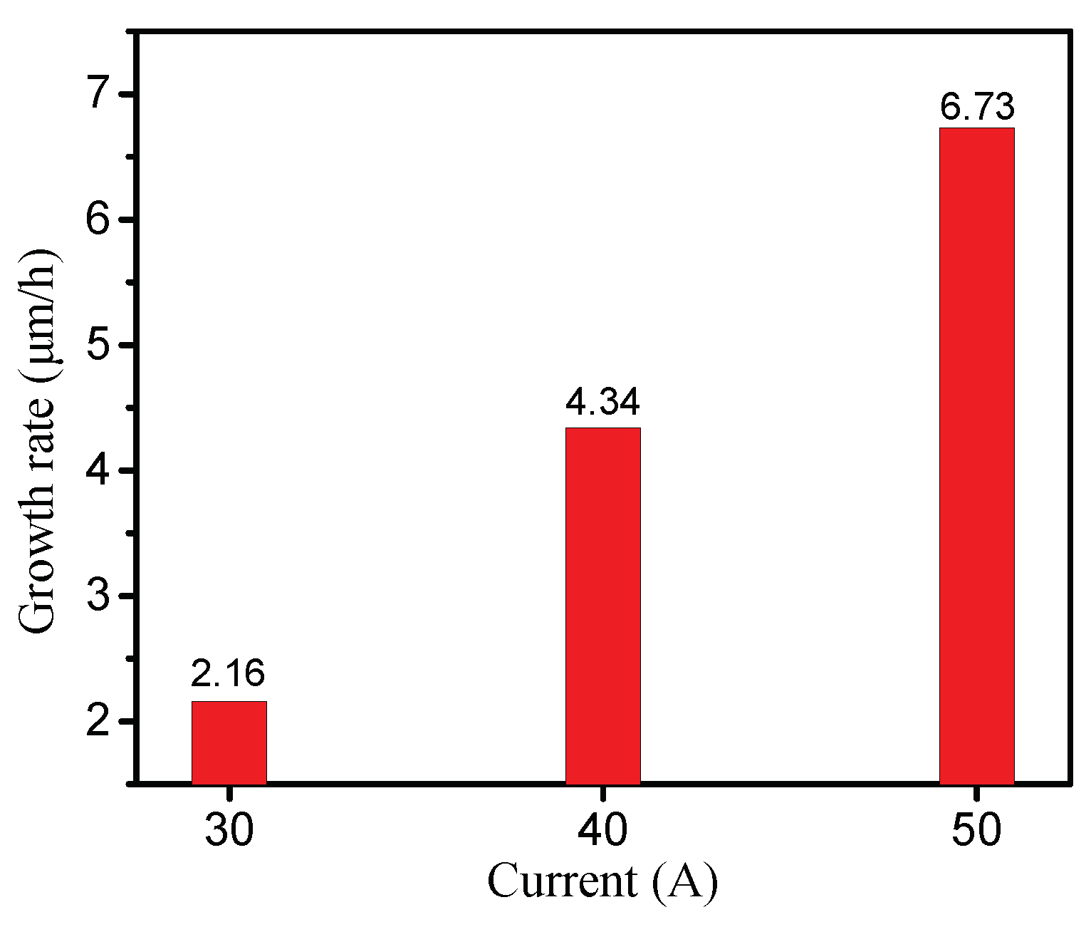
3.3. Effects of Target Current on the Morphology and Growth Rate of ZnO Film

Figure 5 shows the surface and cross-sectional morphologies of the coating deposited with different currents. As the working current increased, the amount of large particle pollutants on the coating surface increased significantly, as well as the particle size. According to the composition analysis, the major particulate pollutants were also Zn metals. The increased current resulted in a large molten pool, which could produce a higher density of large particles. Thus, more particles were observed on the surface. Such large particles typically reduced the compactness of the coating, and could be detrimental to the performance, as they reduced the resistance. From the cross-sectional morphologies and the magnified pictures, coatings presented a columnar grain. These grains became smaller as the current increased, and resulted in obvious compact coatings. In addition, the increased current could greatly increase the deposition rate, which was one of the most important characteristics for application. The deposition rates were calculated via dividing the cross-section thickness (μm) with the deposition time (h), as shown in Figure 6. It increased more than three times as the current increased from 30 to 50 A. The high deposition rate should be related to the high ion density generated via a larger molten poor in the target. Therefore, a high current was better for the deposition efficiency. However, its effects on the resistance and performance need to be further explored.

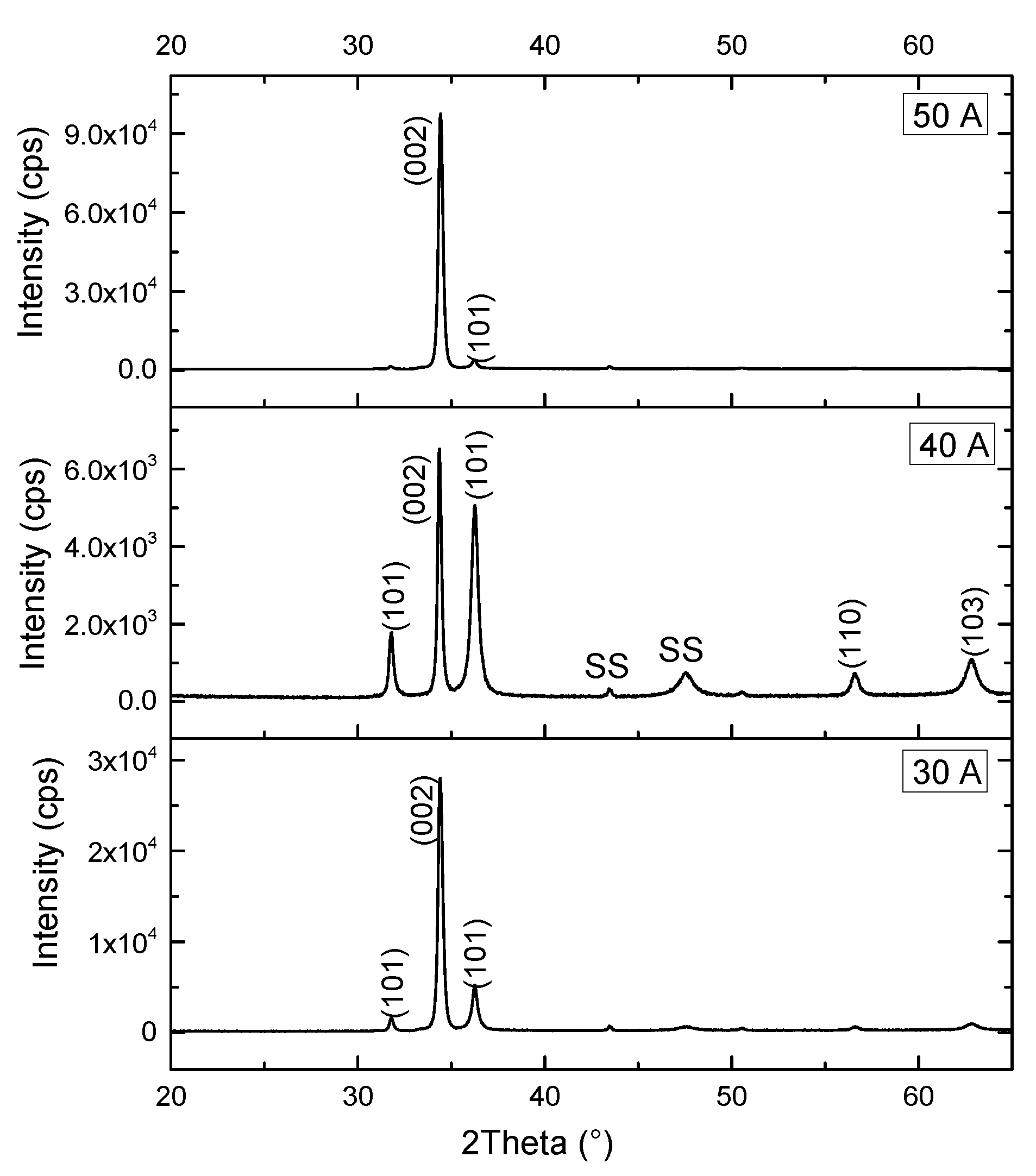
3.4. Effects of Target Currents on Crystal Characteristics and Resistance of ZnO Coatings

The working current not only affected the surface quality of ZnO coatings, but also presented a significant impact on the coating crystal characteristics. Figure 6 showed the structural test results of the coating under different working currents. From the XRD diffraction pattern in Figure 7, coatings deposited with 30 and 40 A revealed three peaks at (100), (002), and (101); (002) was the preferred orientation. The other two peaks dually decreased and disappeared as the current increased to 50 A, which means that the coating changed to grow purely along the c-axis. Based on the analysis of the diffraction peak intensity in Table 2, it can be found that the diffraction peak intensity of the coating also increased with the increase in the working current. The calculated increased FWHM in Table 2 suggested that the crystallization quality of the coating continually improved with the working current. A higher current bestowed higher energy to ions, which allowed more particles to migrate to a location where the surface energy was lower, resulting in a continuous preferential orientation growth in the coating, and a continuous improvement in crystal quality.
The resistance values of the ZnO coatings are shown in Table 2. When the current was 30 A and 50 A, the coating thickness was basically the same, but the resistance values were 400 and 200 KΩ, respectively. This indicates that increasing the working current led to a deterioration in the performance, with a decreased resistance value. The decreased resistance would be the result of the increased particles on the coating surface. However, the maximum resistance of 20 MΩ was obtained in the coating deposited with 40 A, which may be due to the combined effects of coating defects and the coating thickness.

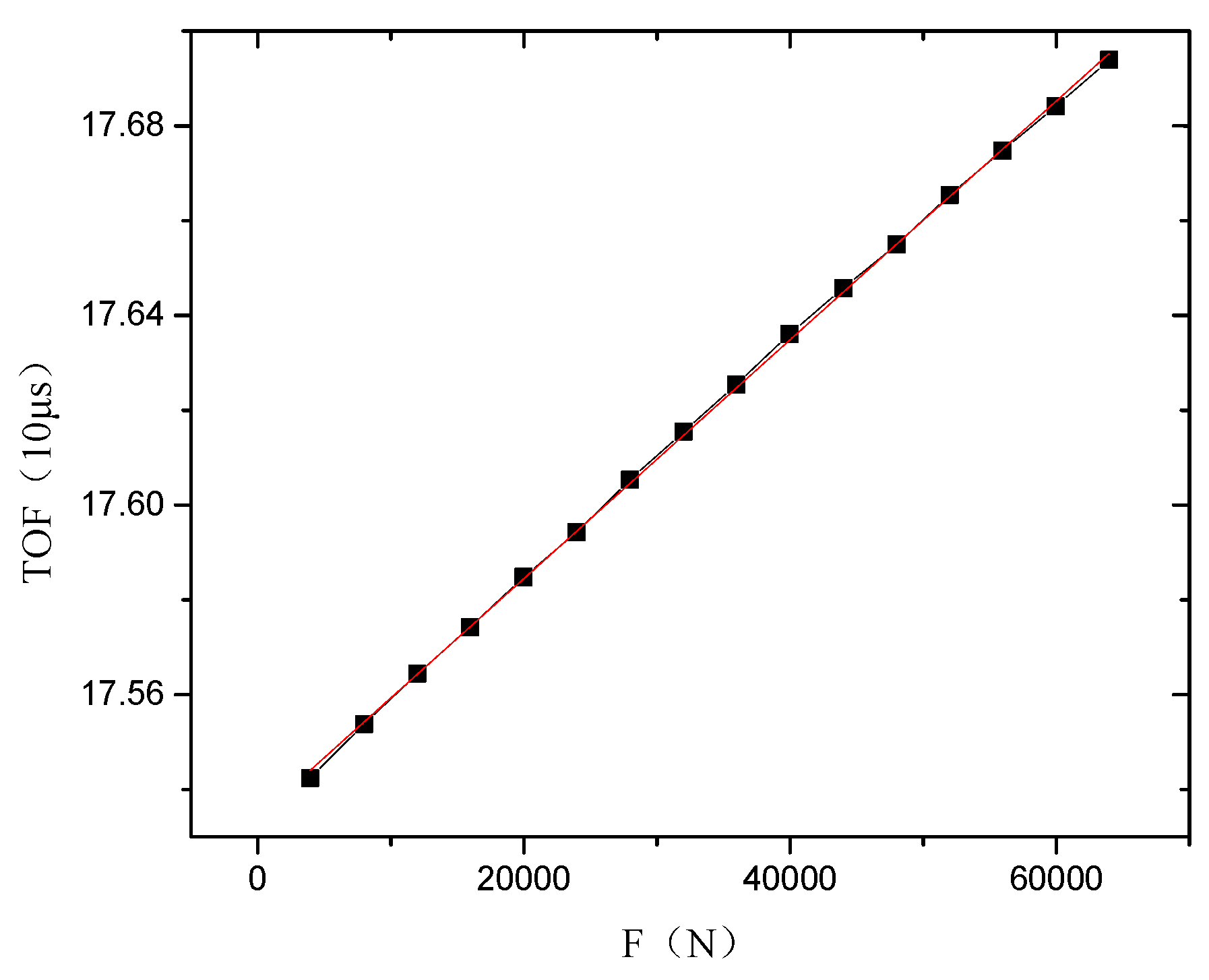
3.5. Performance of Bolt with ZnO Coating Deposited with Optimized Parameters

Based on the above research into the effects of the bias voltage and working current on the crystal structure and resistance of ZnO piezoelectric coatings, a c-axis-preferred-orientated ZnO piezoelectric sensing coating was prepared on the end face of a transformer screw, under the optimized bias voltage of 0 V and current of 40 A. The load and flight time of the screw were calibrated using an ultrasonic system. The relationship could be used to calculate the sound velocity in the stressed screw, to present the stress in the screw. The TOF (time-of-flight) curves, as a function of the load, are shown in Figure 8. The TOF measured via ultrasound presented a good linear relationship with the load when the load ranged from 0 to 64 kN, and the Pearson’s correlation coefficient of the fitting curve reached 99.984%, as shown in Table 3. The results show that the ZnO piezoelectric sensor coating with a high resistance and c-axis-preferred orientation, prepared via the optimal process in this paper, can be used for accurate axial load detection in transformer bolts.

4. Conclusions

In this paper, ZnO piezoelectric sensor coatings for high-voltage intelligent casing bolts were prepared via pulsed arc ion plating. The effects of the bias voltage and current on the growth behaviors and resistance of ZnO piezoelectric sensor coatings were investigated. It was found that the morphology and structure of the coatings were mainly related to the energy of the deposited particles. The higher the bias voltage, the poorer the crystalline quality of the coating, and the lower the resistance value. The resistance greatly decreased from 5.0 KΩ to 0.06 KΩ as the bias voltage increased from 0 to −100 V. Increasing the working current enhanced the orientated growth, but introduced large-metal-particle pollution, which led to the resistance decreasing from 20,000 to 200 KΩ. The bias voltage of 0 V and current of 40 A were beneficial for the preparation of ZnO piezoelectric sensor coatings with a high resistance and c-axis-preferred orientation, resulting in a high Pearson’s correlation coefficient of 99.984% in the monitoring of a load in a screw from 0 to 64 kN. The ZnO coating obtained via this process can be used for accurate axial load detection in transformer bolts. The research results of this paper provide a new idea for the accurate measurement of a bolt preload.

Author Contributions

Conceptualization, D.N.; Methodology, Z.N.; Software, Q.L.; Investigation, J.D.; Data curation, Z.L.; Writing—original draft, H.K. and F.W.; Writing—review & editing, Z.X. All authors have read and agreed to the published version of the manuscript.

Funding

This research received no external funding.

Institutional Review Board Statement

Not applicable.

Informed Consent Statement

Not applicable.

Data Availability Statement

Not applicable.

Conflicts of Interest

Authors Hanpeng Kou, Fuyuan Wang, Dayu Nie, Zhaojun Ning, Qiaoqiao Li, wereemployed by the company State Grid East Inner Mongolia Electric Power Company. Authors Jiangang Deng, Zhenbo Lanand Zhuolin Xu were employed by the company Wuhan NARI Limited Liability Company of State Grid Power Research Institute. The remaining authors declare that the research was conducted in the absence of any commercial or financial relationships that could be construed as a potential conflict of interest.

References

  1. Liu, Z. Characteristics of UHV AC Transmission System. In Ultra-High Voltage Ac/dc Grids; Academic Press: Cambridge, MA, USA, 2015; pp. 35–93. [Google Scholar]
  2. Hashemnia, N.; Abu-Siada, A.; Islam, S. Detection of power transformer bushing faults and oil degradation using frequency response analysis. IEEE Trans. Dielectr. Electr. Insul. 2016, 23, 222–229. [Google Scholar] [CrossRef]
  3. Sikorski, W.; Siodla, K.; Moranda, H.; Ziomek, W. Location of partial discharge sources in power transformers based on advanced auscultatory technique. IEEE Trans. Dielectr. Electr. Insul. 2012, 19, 1948–1956. [Google Scholar] [CrossRef]
  4. Stone, G.C. Partial discharge diagnostics and electrical equipment insulation condition assessment. IEEE Trans. Dielectr. Electr. Insul. 2005, 12, 891–904. [Google Scholar] [CrossRef]
  5. Rosolem, J.B.; Tomiyama, E.K.; Dini, D.C.; Bassan, F.R.; Penze, R.S.; Leonardi, A.A.; Teixeira, R.M. A fiber optic powered sensor designed for partial discharges monitoring on high voltage bushings. In Proceedings of the 2015 SBMO/IEEE MTT-S International Microwave and Optoelectronics Conference (IMOC), Porto de Galinhas, Brazil, 3–6 November 2015; pp. 1–5. [Google Scholar]
  6. Senobari, R.K.; Sadeh, J.; Borsi, H. Frequency response analysis (FRA) of transformers as a tool for fault detection and location: A review. Electr. Power Syst. Res. 2018, 155, 172–183. [Google Scholar] [CrossRef]
  7. Cristaldi, L.; Faifer, M.; Laurano, C.; Ottoboni, R.; Toscani, S. Monitoring of power transformer bushings in high voltage substations. In Proceedings of the 2015 IEEE International Workshop on Applied Measurements for Power Systems (AMPS), Aachen, Germany, 23–25 September 2015; pp. 72–77. [Google Scholar]
  8. Jiang, J.; Ma, G.M.; Song, H.T.; Li, C.R.; Luo, Y.T. Dissolved Hydrogen Sensor in Power Transformer Oil Based on Side Polishing Fiber Bragg Grating. Trans. China Electrotech. Soc. 2017, 13, 264–270. [Google Scholar]
  9. Bodzenta, J.; Burak, B.; Gacek, Z.; Jakubik, W.P.; Kochowski, S.; Urbańczyk, M. Thin palladium film as a sensor of hydrogen gas dissolved in transformer oil. Sens. Actuators B Chem. 2002, 87, 82–87. [Google Scholar] [CrossRef]
  10. Zhang, M.; Shang, R.; Lu, Z.; Zhang, X.; Xie, K.; Zhang, B. Analysis of wind-induced response of down lead transmission line-connection fitting systems in ultrahigh-voltage substations. Eng. Struct. 2020, 206, 110144. [Google Scholar] [CrossRef]
  11. Guo, Y.; Wang, Z.K.; Liu, L. Failure Mechanism Analysis and Preventive Measures of High Voltage Sleeve Head Seal of 500 kV Main Transformer. J. Anhui Electr. Eng. Prof. Tech. Coll. 2017, 22, 38–41. [Google Scholar]
  12. Chen, W.Q.; Shi, M.L.; Shen, Z.Y. Fault Analysis and Improvements on General Cap of Converter Transformer Bushing. Zhejiang Electr. Power 2020, 9, 42–47. [Google Scholar]
  13. Zhu, Z.Q.; Zhou, J.; Liu, G.Z. Research Progress on Growth Methods of ZnO Single Crystal. Chinese J. Rare Met. 2009, 33, 101–106. [Google Scholar]
  14. Jiao, M.Z.; Chen, X.Y.; Hu, K.X.; Qian, D.Y.; Zhao, X.H.; Ding, E.J. Recent developments of nanomaterials-based conductive type methane sensors. Rare Met. 2021, 40, 1515–1527. [Google Scholar] [CrossRef]
  15. Palshikar, A.J.A.Y.; Sharma, N. Review on Piezoelectric Materials as Thin Films with their Applications. Mater. Sci. Res. India 2015, 12, 79–84. [Google Scholar] [CrossRef]
  16. Wang, F. Progress in cathodic arc ion plating technology. Vac. Low Temp. 2020, 26, 87–95. [Google Scholar]
  17. Wang, Z.L.; Song, J. Piezoelectric Nanogenerators Based on Zinc Oxide Nanowire Arrays. Science 2006, 312, 242–246. [Google Scholar] [CrossRef] [PubMed]
  18. Ortiz, T.; Conde, C.; Khan, T.M.; Hussain, B. Thickness uniformity and optical/structural evaluation of RF sputtered ZnO thin films for solar cell and other device applications. Appl. Phys. A 2017, 123, 280. [Google Scholar] [CrossRef]
  19. Hussain, B.; Khan, T.M. Spatial Thickness Uniformity and Structural Evaluation of RF Sputtered ZnO Thin Films for Solar Cell. In Proceedings of the 2017 IEEE 44th Photovoltaic Specialist Conference (PVSC), Washington, DC, USA, 25–30 June 2017; pp. 451–454. [Google Scholar]
Figure 1. Schematics and photos showing the coating location and fixing; (a) bolt with coatings, (b) Schematic of the coating position; (c) tensile test of the bolt.
Coatings 13 01662 g001
Figure 2. Surface and cross-sectional morphologies of ZnO coatings under different bias voltages: (a,d) 0 V; (b,e) −50 V; (c,f) −100 V, (a), (b), (c) are images with low magnification corresponded to (ac).
Coatings 13 01662 g002
Figure 3. Contents of Zn and O in ZnO coatings under different bias voltages.
Coatings 13 01662 g003
Figure 4. XRD patterns of ZnO coatings deposited with different bias voltages.
Coatings 13 01662 g004
Figure 5. Surface and cross-sectional morphologies of ZnO coatings under different working currents: (a,d) 30 A; (b,e) 40 A; (c,f) 50 A; (a), (b), (c) are images with low magnification corresponded to (ac).
Coatings 13 01662 g005
Figure 6. Deposition rates of ZnO coatings under different working currents.
Coatings 13 01662 g006
Figure 7. XRD patterns of ZnO coatings deposited at different working currents.
Coatings 13 01662 g007
Figure 8. The load–TOF curves of the bolt with coatings deposited at 0 V and 40 A.
Coatings 13 01662 g008
Table 1. Crystalline characteristics and resistance of ZnO coatings deposited at different bias voltages.
Bias Voltage (V)0−50−100
Intensity (cps)207,689168,216485
FWHM0.30.360.91
Resistance (KΩ)5.00.20.06
Table 2. Crystalline characteristics and resistance of ZnO coatings deposited at different working currents.
Working Current (A)304050
Orientation coeffeicient0.470.81
Intensity (cps.)615028,01697,499
FWHM0.280.2680.203
Resistance (KΩ)40020,000200
Table 3. Fitting results of the load–TOF curve.
Equationy = a + b*x
Pearson’s r0.99985
Adj. R-squared0.99967
ValueStandard error
BIntercept17.534124.54419 × 10−4
Slope2.51855 × 10−61.17561 × 10⁻⁸
Disclaimer/Publisher’s Note: The statements, opinions and data contained in all publications are solely those of the individual author(s) and contributor(s) and not of MDPI and/or the editor(s). MDPI and/or the editor(s) disclaim responsibility for any injury to people or property resulting from any ideas, methods, instructions or products referred to in the content.

