
The Contribution of the Pore Size of Titanium DC (Direct Current) Sputtered Condensation Polymer Materials to Electromagnetic Interruption and Thermal Properties
Abstract
:1. Introduction
2. Materials and Methods
3. Results and Discussions
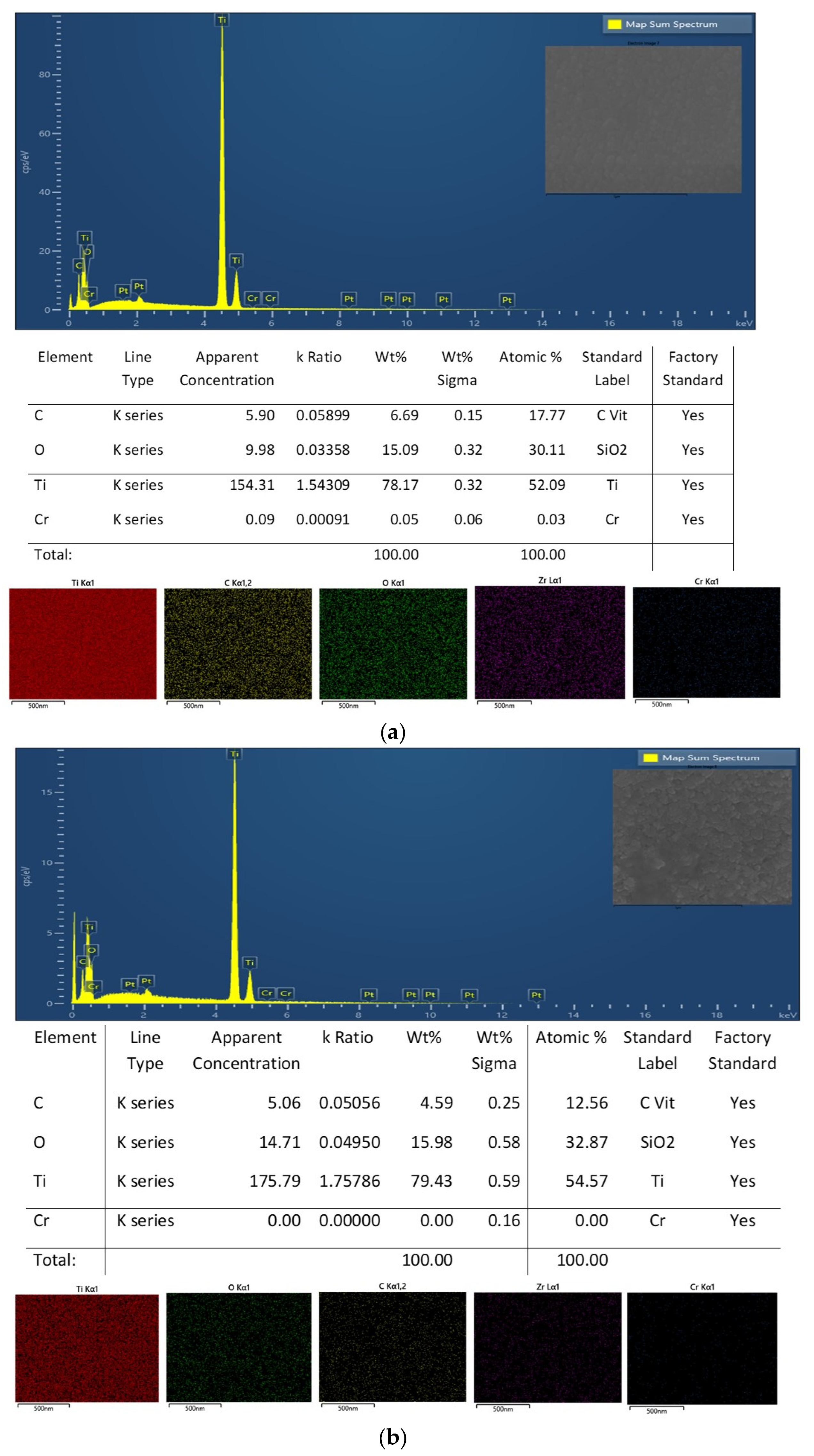
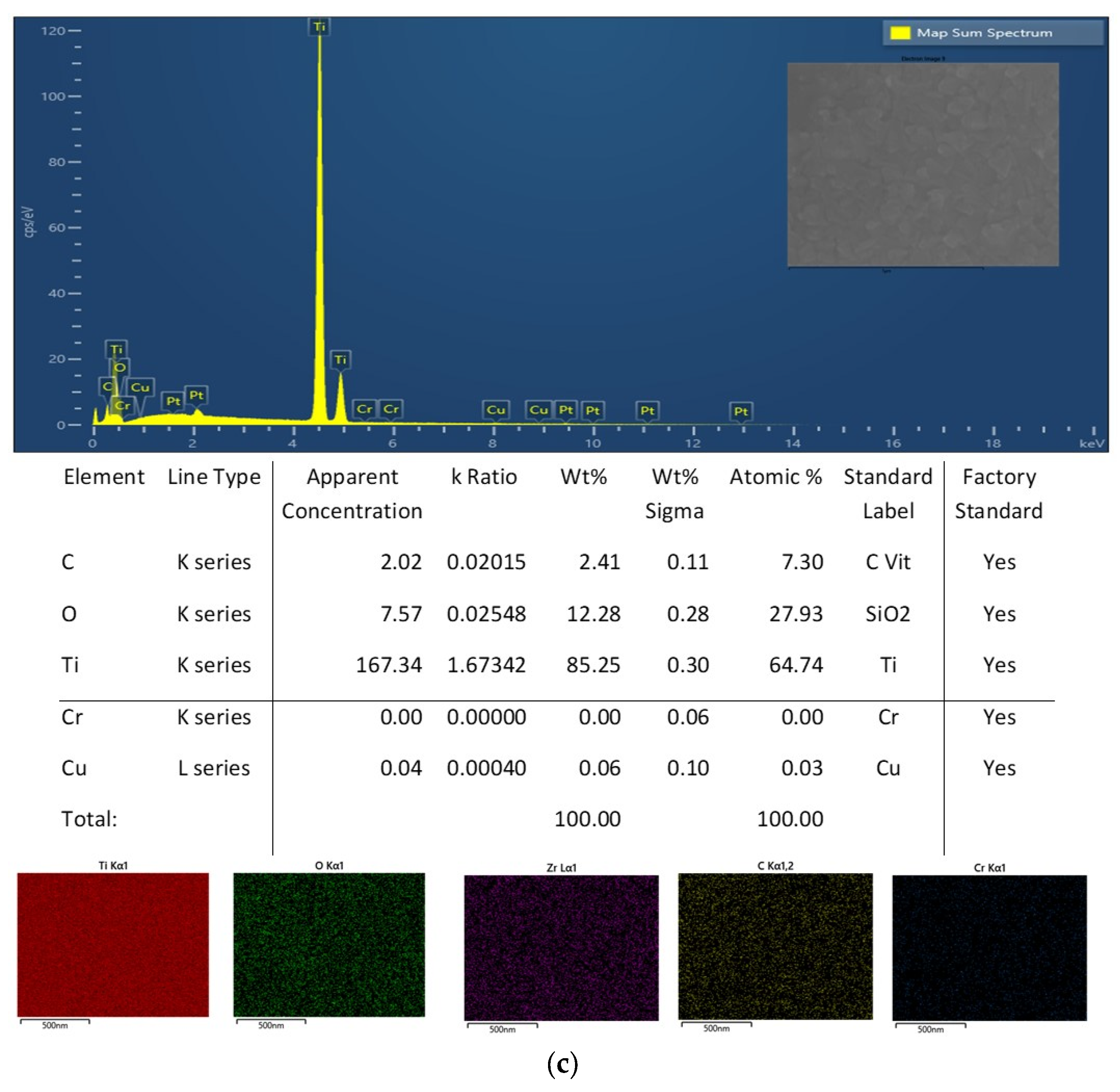
3.1. Surface Geometry
3.2. Characteristics of Electromagnetic Interference
3.3. Characteristics of Electrical Conductivity
3.4. Infrared Transmittance Behavior
3.5. Infrared Image Stealth Characteristics According to Heat Transfer at High Temperature
4. Conclusions
Funding
Institutional Review Board Statement
Informed Consent Statement
Data Availability Statement
Conflicts of Interest
References
- Chen, H.; Feng, R.; Xia, T.; Wen, Z.; Li, Q.; Qiu, X.; Huang, B.; Li, Y. Progress in Surface Modification of Titanium Implants by Hydrogel Coatings. Gels 2023, 9, 423. [Google Scholar] [CrossRef] [PubMed]
- Chumaevskii, A.; Amirov, A.; Ivanov, A.; Rubtsov, V.; Kolubaev, E. Friction Stir Welding/Processing of Various Metals with Working Tools of Different Materials and Its Peculiarities for Titanium Alloys: A Review. Metals 2023, 13, 970. [Google Scholar] [CrossRef]
- Guo, A.X.Y.; Cao, B.; Wang, Z.; Ma, X.; Cao, S.C. Fabricated High-Strength, Low-Elastic Modulus Biomedical Ti-24Nb-4Zr-8Sn Alloy via Powder Metallurgy. Materials 2023, 16, 3845. [Google Scholar] [CrossRef] [PubMed]
- Jażdżewska, M.; Bartmański, M.; Zieliński, A.; Kwidzińska, D.B. Effect of Laser Treatment on Intrinsic Mechanical Stresses in Titanium and Some of Its Alloys. Appl. Sci. 2023, 13, 6276. [Google Scholar] [CrossRef]
- Kovács, Á.É.; Csernátony, Z.; Csámer, L.; Méhes, G.; Szabó, D.; Veres, M.; Braun, M.; Harangi, B.; Serbán, N.; Zhang, L.; et al. Comparative Analysis of Bone Ingrowth in 3D-Printed Titanium Lattice Structures with Different Patterns. Materials 2023, 16, 3861. [Google Scholar] [CrossRef] [PubMed]
- Lu, X.; Shu, C.; Zheng, Z.; Shu, X.; Chen, S.; Essa, K.; Li, Z.; Xu, H. Effects of L-PBF Scanning Strategy and Sloping Angle on the Process Properties of TC11 Titanium Alloy. Metals 2023, 13, 983. [Google Scholar] [CrossRef]
- Nazarov, D.; Kozlova, L.; Rudakova, A.; Zemtsova, E.; Yudintceva, N.; Ovcharenko, E.; Koroleva, A.; Kasatkin, I.; Kraeva, L.; Rogacheva, E.; et al. Atomic Layer Deposition of Chlorine Containing Titanium–Zinc Oxide Nanofilms Using the Supercycle Approach. Coatings 2023, 13, 960. [Google Scholar]
- Pietzka, S.; Wenzel, M.; Winter, K.; Wilde, F.; Schramm, A.; Ebeling, M.; Kasper, R.; Scheurer, M.; Sakkas, A. Comparison of Anatomical Preformed Titanium Implants and Patient-Specific CAD/CAM Implants in the Primary Reconstruction of Isolated Orbital Fractures—A Retrospective Study. J. Pers. Med. 2023, 13, 846. [Google Scholar]
- Rodríguez-Contreras, A.; Torres, D.; Piñera-Avellaneda, D.; Pérez-Palou, L.; Ortiz-Hernández, M.; Ginebra, M.P.; Calero, J.A.; Manero, J.M.; Rupérez, E. Dual-Action Effect of Gallium and Silver Providing Osseointegration and Antibacterial Properties to Calcium Titanate Coatings on Porous Titanium Implants. Int. J. Mol. Sci. 2023, 24, 8762. [Google Scholar] [CrossRef]
- Xing, L.; Song, H.; Wei, J.; Wang, X.; Yang, Y.; Zhe, P.; Luan, M.; Xu, J. Influence of a Composite Polylysine-Polydopamine-Quaternary Ammonium Salt Coating on Titanium on Its Ostogenic and Antibacterial Performance. Molecules 2023, 28, 4120. [Google Scholar] [CrossRef]
- Zhang, Q.; Chen, Y.; Li, B.; Wang, C.; Wu, L.; Yao, J. Tribological Behavior of Ti-Coated Diamond/Copper Composite Coating Fabricated via Supersonic Laser Deposition. Lubricants 2023, 11, 216. [Google Scholar] [CrossRef]
- Zuo, S.; Wang, L.; Zhang, J.; Yang, G.; Xu, Y.; Hu, Y.; Cheng, F.; Hu, X. Comparative Study of Resin and Silane Coupling Agents Coating Treatments on Bonding Strength Improvement of Titanium and Carbon Fiber Composites. Coatings 2023, 13, 903. [Google Scholar] [CrossRef]
- Aljaafari, A.; Ahmed, F.; Shaalan, N.M.; Kumar, S.; Alsulami, A. Enhanced Thermal Stability of Sputtered TiN Thin Films for Their Applications as Diffusion Barriers against Copper Interconnect. Inorganics 2023, 11, 204. [Google Scholar] [CrossRef]
- Cui, C.; Yang, C. Mechanical Properties and Wear Resistance of CrSiN Coating Fabricated by Magnetron Sputtering on W18Cr4V Steel. Coatings 2023, 13, 889. [Google Scholar] [CrossRef]
- Eleutério, T.; Sério, S.; Vasconcelos, H.C. Growth of Nanostructured TiO2 Thin Films onto Lignocellulosic Fibers through Reactive DC Magnetron Sputtering: A XRD and SEM Study. Coatings 2023, 13, 922. [Google Scholar] [CrossRef]
- Ju, Y.; Ai, L.; Qi, X.; Li, J.; Song, W. Review on Hydrophobic Thin Films Prepared Using Magnetron Sputtering Deposition. Materials 2023, 16, 3764. [Google Scholar] [CrossRef] [PubMed]
- Kotliarenko, A.; Azzolini, O.; Cisternino, S.; El Idrissi, M.; Esposito, J.; Keppel, G.; Pira, C.; Taibi, A. First Results on Zinc Oxide Thick Film Deposition by Inverted Magnetron Sputtering for Cyclotron Solid Targets Production. Materials 2023, 16, 3810. [Google Scholar] [CrossRef] [PubMed]
- Pang, Y.; Zhao, N.; Ruan, Y.; Sun, L.; Zhang, C. Effects of Oxygen Partial Pressure and Thermal Annealing on the Electrical Properties and High-Temperature Stability of Pt Thin-Film Resistors. Chemosensors 2023, 11, 285. [Google Scholar] [CrossRef]
- Pokora, P.; Wojcieszak, D.; Mazur, P.; Kalisz, M.; Sikora, M. Influence of Co-Content on the Optical and Structural Properties of TiOx Thin Films Prepared by Gas Impulse Magnetron Sputtering. Coatings 2023, 13, 955. [Google Scholar] [CrossRef]
- Rocha-Cuervo, J.J.; Uribe-Lam, E.; Treviño-Quintanilla, C.D.; Melo-Maximo, D.V. Sputtering Plasma Effect on Zinc Oxide Thin Films Produced on Photopolymer Substrates. Polymers 2023, 15, 2283. [Google Scholar] [CrossRef]
- Sasani Ghamsari, M. Development of Thin Film Fabrication Using Magnetron Sputtering. Metals 2023, 13, 963. [Google Scholar] [CrossRef]
- Bochenek, D.; Chrobak, A.; Ziółkowski, G. Electric and Magnetic Properties of the Multiferroic Composites Made Based on Pb(Fe1/2Nb1/2)1−xMnxO3 and the Nickel-Zinc Ferrite. Materials 2023, 16, 3785. [Google Scholar] [PubMed]
- Mi, D.; Zhao, Z.; Bai, H. Effects of Orientation and Dispersion on Electrical Conductivity and Mechanical Properties of Carbon Nanotube/Polypropylene Composite. Polymers 2023, 15, 2370. [Google Scholar] [CrossRef] [PubMed]
- Mollamohammadi, F.; Faridnouri, H.; Zare, E.N. Electrochemical Biosensing of L-DOPA Using Tyrosinase Immobilized on Carboxymethyl Starch-Graft-Polyaniline@MWCNTs Nanocomposite. Biosensors 2023, 13, 562. [Google Scholar] [CrossRef] [PubMed]
- Nguyen, Q.T.; Vu, D.L.; Le, C.D.; Ahn, K.K. Enhancing the Performance of Triboelectric Generator: A Novel Approach Using Solid–Liquid Interface-Treated Foam and Metal Contacts. Polymers 2023, 15, 2392. [Google Scholar] [PubMed]
- Regis, V.; Šadl, M.; Brennecka, G.; Bradeško, A.; Tomc, U.; Uršič, H. Investigation of Structural and Electrical Properties of Al2O3/Al Composites Prepared by Aerosol Co-Deposition. Crystals 2023, 13, 850. [Google Scholar] [CrossRef]
- Stefano, M.; Cordella, F.; Cozza, G.; Ciancio, A.L.; Zollo, L. Study of Electrical Neural Stimulation Effects Using Extraneural and Intraneural Electrodes. Appl. Sci. 2023, 13, 6267. [Google Scholar] [CrossRef]
- Thangamani, G.; Thangaraj, M.; Anand, P.I.; Mani, J.; Karkalos, N.E.; Papazoglou, E.L.; Karmiris-Obratański, P. Influence of Silver-Coated Tool Electrode on Electrochemical Micromachining of Incoloy 825. Coatings 2023, 13, 963. [Google Scholar] [CrossRef]
- Lu, Q.; Han, Z.; Hu, L.; Tian, F. An Infrared and Visible Image Fusion Algorithm Method Based on a Dual Bilateral Least Squares Hybrid Filter. Electronics 2023, 12, 2292. [Google Scholar] [CrossRef]
- Lv, J.; Hui, T.; Zhi, Y.; Xu, Y. Infrared Image Caption Based on Object-Oriented Attention. Entropy 2023, 25, 826. [Google Scholar] [CrossRef]
- Xu, X.; Shen, Y.; Han, S. Dense-FG: A Fusion GAN Model by Using Densely Connected Blocks to Fuse Infrared and Visible Images. Appl. Sci. 2023, 13, 4684. [Google Scholar] [CrossRef]
- Zhao, L.; Jiao, J.; Yang, L.; Pan, W.; Zeng, F.; Li, X.; Chen, F. A CNN-Based Layer-Adaptive GCPs Extraction Method for TIR Remote Sensing Images. Remote Sens. 2023, 15, 2628. [Google Scholar] [CrossRef]
- Han, H.R. Stealth, electromagnetic interception, and electrical properties of aluminum sputtered clothing materials—Focusing on the density change. Costume Cult. Res. 2022, 30, 579. [Google Scholar] [CrossRef]


| Poly Amide Film | Poly Amide Fabric | Poly Amide Net 1 | Poly Amide Net 2 | Poly Amide Net 3 | Poly Amide Net 4 | Poly Amide Net 5 | |
|---|---|---|---|---|---|---|---|
| Sample code | TF1 | TA1 | TN1 | TN2 | TN3 | TN4 | TN5 |
| Sample thickness (mm) | 0.09 | 0.15 | 0.08 | 0.10 | 0.15 | 0.11 | 0.19 |
| Weave type | Film | Plain weave | Plain mesh | Plain mesh | Plain mesh | Plain mesh | Plain mesh |
| Pore size (μm2) | 0 | 1200 | 3564 | 35,696.3 | 94,440.4 | 136,476.2 | 294,825.5 |
| Time (s) | 2400 |
| Process pressure (Torr) | 6 m |
| Gas (sccm) | Ar 40 |
| Power (W) | DC 600 |
| Machine | SRN-120 |
| Untreated | Titanium Phase: Up | Titanium Phase: Down | |||||||
|---|---|---|---|---|---|---|---|---|---|
| H | S | V | H | S | V | H | S | V | |
| TF1 | 72 | 12 | 92 | 280 | 55 | 61 | 57 | 49 | 87 |
| TA1 | 47 | 69 | 93 | 345 | 51 | 79 | 52 | 58 | 91 |
| TN1 | 60 | 28 | 89 | 37 | 93 | 96 | 62 | 34 | 89 |
| TN2 | 60 | 27 | 92 | 39 | 82 | 89 | 55 | 59 | 91 |
| TN3 | 60 | 35 | 90 | 44 | 81 | 92 | 52 | 73 | 92 |
| TN4 | 56 | 38 | 91 | 45 | 85 | 93 | 62 | 27 | 90 |
| TN5 | 49 | 69 | 92 | 47 | 84 | 91 | 57 | 48 | 90 |
| Titanium Phase: Up | Titanium Phase: Down | |||||||
|---|---|---|---|---|---|---|---|---|
| ΔH | ΔS | ΔV | ΔE | ΔH | ΔS | ΔV | ΔE | |
| TF1 | 208 | 43 | −31 | 214.6 | −15 | 37 | −5 | 40.2 |
| TA1 | 298 | −18 | −14 | 298.9 | 5 | −11 | −2 | 12.2 |
| TN1 | −23 | 65 | 7 | 69.3 | 2 | 6 | 0 | 6.3 |
| TN2 | −21 | 55 | −3 | 58.9 | −5 | 32 | −1 | 32.4 |
| TN3 | −16 | 46 | 2 | 48.7 | −8 | 38 | 2 | 38.9 |
| TN4 | −11 | 47 | 2 | 48.3 | 6 | −11 | −1 | 12.6 |
| TN5 | −2 | 15 | −1 | 15.2 | 8 | −21 | −2 | 22.6 |
| Untreated | Titanium Phase: Up | Titanium Phase: Down | |||||||
|---|---|---|---|---|---|---|---|---|---|
| Y | Cb | Cr | Y | Cb | Cr | Y | Cb | Cr | |
| TF1 | 228 | −13 | −4 | 55 | 52 | 35 | 199 | −76 | 25 |
| TA1 | 194 | −83 | 29 | 113 | −11 | 64 | 204 | −68 | 20 |
| TN1 | 217 | −28 | 2 | 166 | −89 | 57 | 212 | −45 | 7 |
| TN2 | 231 | −32 | 7 | 176 | −90 | 49 | 204 | −72 | 19 |
| TN3 | 223 | −35 | 3 | 186 | −94 | 37 | 201 | −72 | 17 |
| TN4 | 212 | −49 | 12 | 181 | −88 | 39 | 221 | −42 | 9 |
| TN5 | 202 | −76 | 27 | 192 | −90 | 32 | 216 | −59 | 12 |
| Titanium Phase: Up | Titanium Phase: Down | |||||||
|---|---|---|---|---|---|---|---|---|
| ΔY | ΔCb | ΔCr | ΔT | ΔY | ΔCb | ΔCr | ΔT | |
| TF1 | −173 | 65 | 39 | 188.9 | −29 | −63 | 29 | 75.2 |
| TA1 | −81 | 72 | 35 | 113.9 | 10 | 15 | −9 | 20.1 |
| TN1 | −51 | −61 | 55 | 96.7 | −5 | −17 | 5 | 18.4 |
| TN2 | −55 | −58 | 42 | 90.3 | −27 | −40 | 12 | 49.7 |
| TN3 | −37 | −59 | 34 | 77.5 | −22 | −37 | 14 | 45.3 |
| TN4 | −31 | −39 | 27 | 56.7 | 9 | 7 | −3 | 11.8 |
| TN5 | −10 | −14 | 5 | 17.9 | 14 | 17 | −15 | 26.6 |
| Pore Size of Sputtered Specimens (μm2) | Electromagnetic Field of Titanium Phase Up (V/m) | Electrical Resistance (kΩ) | IR Transmittance of Titanium Phase Front (%) | Surface Temperature of Titanium Phase Up (°C) | ΔE Value of Titanium Phase Up | ΔT Value of Titanium Phase Up |
|---|---|---|---|---|---|---|
| 0 | 64.0 | 2.4 | 0 | 32.5 | 214.6 | 188.9 |
| 1200 | 142.0 | 1000.0 | 0.7 | 38.5 | 298.9 | 113.9 |
| 3564 | 143.3 | 5.6 | 37.1 | 41.4 | 69.3 | 96.7 |
| 35,696 | 151.7 | 164.0 | 43.9 | 41.6 | 58.9 | 90.3 |
| 94,440 | 178.3 | 429.5 | 63.5 | 42.6 | 48.7 | 77.5 |
| 136,476 | 165.7 | 1.4 | 57.3 | 43.2 | 48.3 | 56.7 |
Disclaimer/Publisher’s Note: The statements, opinions and data contained in all publications are solely those of the individual author(s) and contributor(s) and not of MDPI and/or the editor(s). MDPI and/or the editor(s) disclaim responsibility for any injury to people or property resulting from any ideas, methods, instructions or products referred to in the content. |
© 2023 by the author. Licensee MDPI, Basel, Switzerland. This article is an open access article distributed under the terms and conditions of the Creative Commons Attribution (CC BY) license (https://creativecommons.org/licenses/by/4.0/).
Share and Cite
Han, H.-R. The Contribution of the Pore Size of Titanium DC (Direct Current) Sputtered Condensation Polymer Materials to Electromagnetic Interruption and Thermal Properties. Coatings 2023, 13, 1756. https://doi.org/10.3390/coatings13101756
Han H-R. The Contribution of the Pore Size of Titanium DC (Direct Current) Sputtered Condensation Polymer Materials to Electromagnetic Interruption and Thermal Properties. Coatings. 2023; 13(10):1756. https://doi.org/10.3390/coatings13101756
Chicago/Turabian StyleHan, Hye-Ree. 2023. "The Contribution of the Pore Size of Titanium DC (Direct Current) Sputtered Condensation Polymer Materials to Electromagnetic Interruption and Thermal Properties" Coatings 13, no. 10: 1756. https://doi.org/10.3390/coatings13101756
APA StyleHan, H.-R. (2023). The Contribution of the Pore Size of Titanium DC (Direct Current) Sputtered Condensation Polymer Materials to Electromagnetic Interruption and Thermal Properties. Coatings, 13(10), 1756. https://doi.org/10.3390/coatings13101756