Article

Influence of Electron Beam Treatment on Structure and Phase Composition of TiB2–Ag Coating Deposited by Electrical Explosion Spraying

by
Artem D. Filyakov
1,*,
Vasilii V. Pochetukha
2,
Denis A. Romanov
1 and
Ekaterina S. Vashchuk
2
1
Laboratory of Scanning Electron Microscopy and Image Processing, Siberian State Industrial University, Novokuznetsk 654007, Russia
2
Scientific Research Department, Siberian State Industrial University, Novokuznetsk 654007, Russia
*
Author to whom correspondence should be addressed.
Coatings 2023, 13(11), 1867; https://doi.org/10.3390/coatings13111867
Submission received: 6 October 2023 / Revised: 26 October 2023 / Accepted: 29 October 2023 / Published: 31 October 2023
(This article belongs to the Special Issue Electron-Ion-Plasma Technology Applied to Surface Engineering)

Abstract

:
Due to many factors, the electrical explosion spraying process is not stable, which directly causes unstable coating quality and structure. Electron beam treatment may be used to improve the surface and modified structure of coatings sprayed by electrical explosions. In this study, a new TiB2–Ag metal matrix composite coating was deposited by electrical explosion spraying and modified by electron beam treatment. The prepared coatings were characterized by surface macro- and microanalysis, XDR, cross-section SEM, and TEM. The composition of the spray-coating phase differs from sample to sample. The electron beam treatment normalized the phase composition. Ag TiB2 B2O became the main phase in the modified coating. Increasing the pulse energy density and duration leads to a reduction in the low-melting Ag phase and the formation of copper contact phases due to heating and melting of the copper substrate by excess electron beam energy. The coating structure consists of a silver matrix and TiB2 inclusions. The electron beam treatment did not affect the structure; however, the microstructure of the coating transformed into a cellular crystallization structure. The silver matrix nanostructure was transformed into a nanocrystalline structure with an average crystal size ranging from tens to hundreds of nanometers.

1. Introduction

Moving electrical contacts is crucial for safety in modern power management systems [1]. The wide diversity of their application ranges from low-voltage to high-voltage power networks [2]. Future automated control systems will increase the number of terminals and sensors containing electrical contacts. Their trouble-free operation guarantees the system’s reliability [3]. Therefore, improving the contact material properties in such devices is an important task for materials engineering [1].
Electrical contact materials should have certain characteristics, such as high thermal and electrical conductivity, resistance to oxidation, melting point, hardness, and low vapor [4].
An example of such materials is silver base materials, widely used in low-voltage devices [5]. Pure silver has relatively high thermal and electrical conductivity but has poor erosion resistance, welding, and mechanical properties [6]. Hence, different materials are added to pure silver to improve it by forming alloys or composite materials [1]. Opposed to alloys, there is no or limited solubility of silver in the reinforcement phase in metal matrix composite. Thus, the individual phases retain their respective thermal and electrical properties [7]. The metal matrix provides high electrical and thermal conductivity in this case, whereas the reinforcement phase gives strength, welding, and erosion resistance [8].
AgCdO contact material has good performance, especially excellent arc extinction, and low cost [9,10]. However, due to the harmful nature to the environment and human health of cadmium oxide (CdO), European environmental legislation End-of-Life Vehicle (ELV) and Restrictions of Hazardous Substances (RoHS) restricted its applications [11].
Hence, new electrical contact materials should be environmentally friendly and CdO-free [12]. Currently, there are many silver-based contact material alternatives, such as AgSnO2, Ag–ZnO, and many others. Yet, AgSnO2 contact materials suffer from poor workability, poor conduct at high temperatures, and high contact resistance [12]. Compared to AgSnO2, Ag–ZnO material decomposition is more difficult under the same exploitation due to the high melting point of ZnO. Moreover, the ZnO particles effectively protect against silver sputtering. However, apart from possessing low contact resistance, Ag–ZnO materials have unsatisfactory resistance to welding and a greater tendency to contact wear [13].
One of the promising materials as a reinforcement phase for Ag matrix contact materials is TiB2. Titanium diboride exhibits a high melting point (over 2900 °C), high hardness (30 GPa), and good thermal conductivity (25 J/A.D.F.K). The most important is that it has the lowest resistivity among superhard ceramic materials (9 μΩ cm2) [14].
In the study of [15], the AgTiB2 composites were prepared by high-energy milling and powder metallurgy. The achieved material can be utilized as a potential contact material. However, researchers admit that there is a necessity to improve production parameters to promote the interface bond strength between Ag and TiB2. The article of [16] shows that the Ag–4wt.%TiB2 contact material presents higher make-arc-energy and lower break-arc-energy than the Ag–4wt.%SnO2 contact material. The research of [17] demonstrates that the Ag–4wt.%TiB2 contact material presents a lower relative transfer mass than the Ag–4wt.%SnO2 contact material.
However, silver by itself is a relatively expensive material; on the other hand, copper is relatively cheap and has the best electrical conductivity after silver; however, it has lower oxidation resistance [18]. The use of copper plated with silver-based coating instead of silver-based electrical contact is more rational from an economic point of view. Their cost is much lower due to using small amounts of silver [19,20].
The type of thermal spraying technique is that which utilizes the instantaneous discharge of metal conductors to produce dynamic shock waves that spray high-speed electrical explosion products onto the substrate’s surface to form a coating [21,22]. This kind of thermal spraying has some limitations and disadvantages. The metal conductor should be produced from thin foils, wires, or fine powder to achieve instantaneous discharge. The electrical explosion spraying process requires composite large-thickness conductors made of multiple foil layers and powder for the production of composite coatings. Increasing the conductor’s thickness leads to insufficient heating, non-synchronous explosion, and different-sized larger solid particles forming during the explosion [23], which directly causes unstable coating quality and structure. Electron beam treatment may be used to improve the surface and modified structure of the coating sprayed by electrical explosion.
Thus, based on the above, the present work aims to investigate the influence of electron beam treatment on the structure and phase composition of TiB2–Ag coating prepared by electrical explosion.

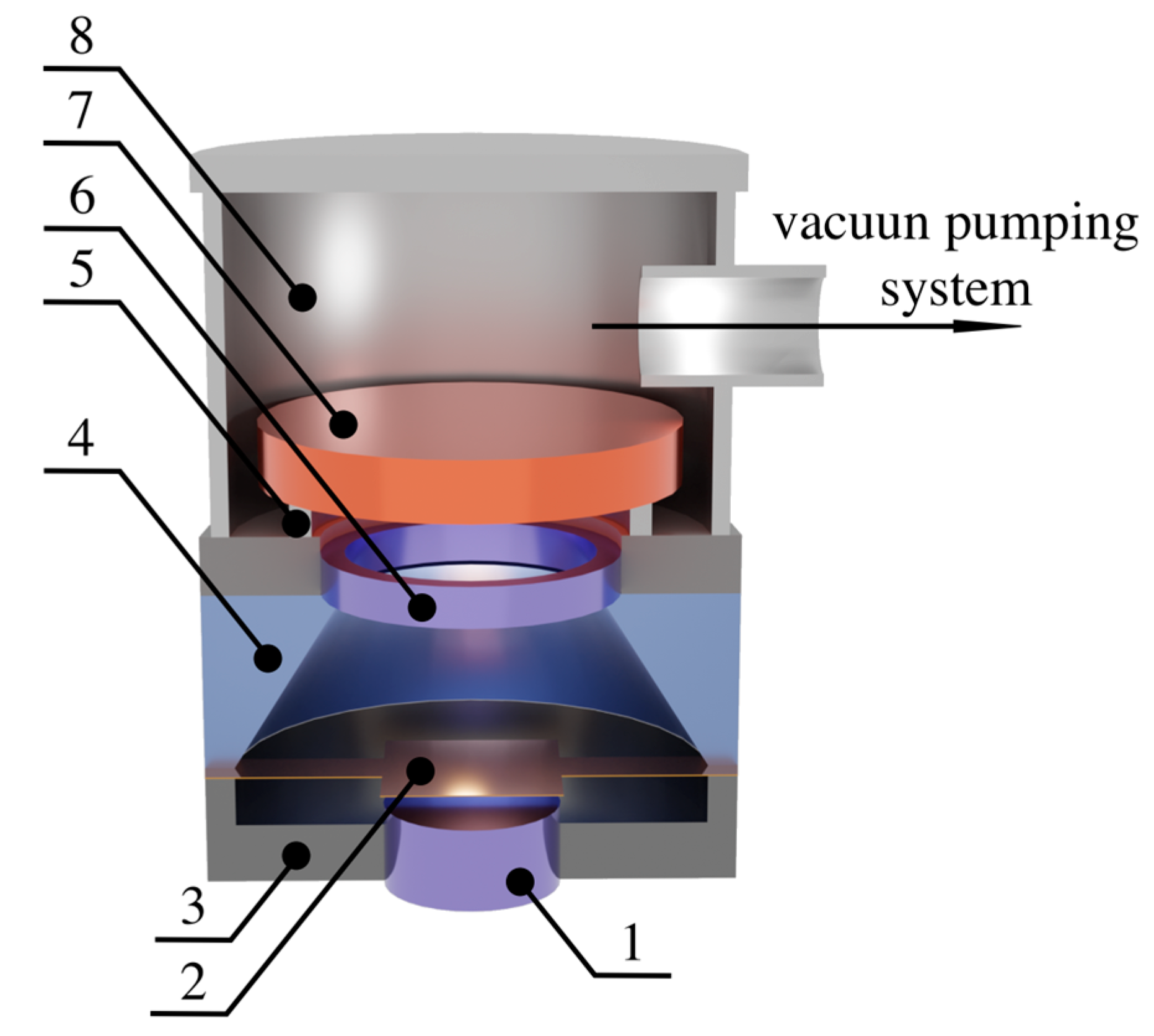
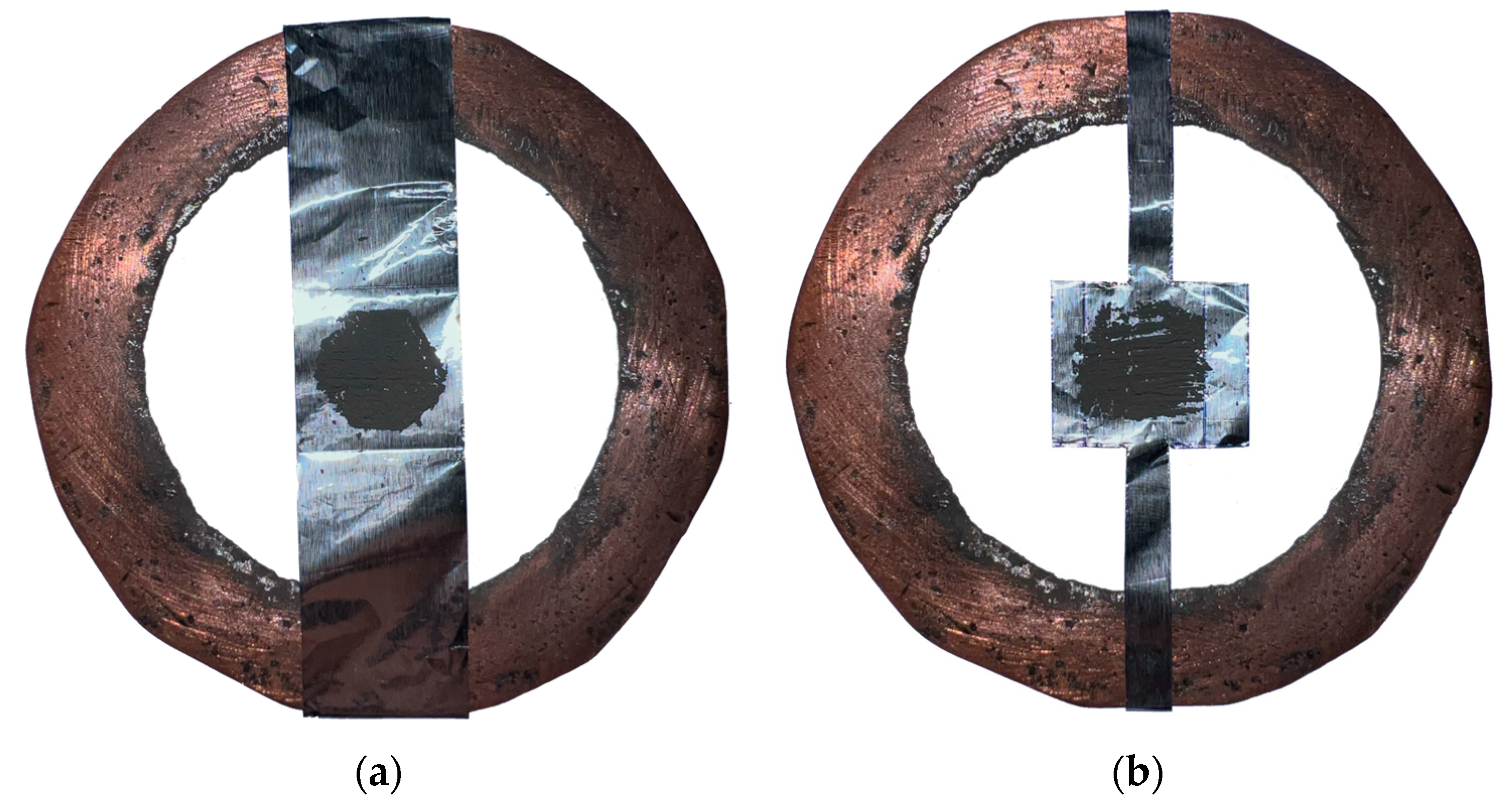
2. Materials and Methods

TiB2–Ag coating was sprayed by electrical explosion spraying on the copper substrate (electrical copper of grade M00). The experimental electrical explosive spraying machine EVU 60/10 M was used for coating spraying. The experimental spraying machine was designed by the authors. Structurally, it consists of a charger, capacitive energy storage, and plasma accelerator.
The plasma accelerator design is shown in Figure 1. There are inner cylindrical 1 and outer ring 6 electrodes separated by an insulating insert 3 and discharge working chamber (nozzle) 4. The high-density current generated by the pulse discharge exploded composite conductor 2 via ohmic heating. The explosion products blast into vacuum chamber 8 with a pressure of 100 Pa and are then sprayed onto the sample’s surface 7 fixed in holder 5 at a certain distance from the nozzle.
The electric explosion provided on the surface of the treated material an absorbed power density of 5.5 GW/m2, pressure in a shock-compressed layer near a surface being irradiated of ~12.5 MPa, residual gas pressure in a working chamber of ~100 Pa, plasma temperature on nozzle cut of ~104 K, and pulse time of ~100 μs.
The electrical explosion product is a multi-component plasma jet. The high-temperature shocked layer with high pressure formed by leakage and reflection of supersonic plasma jet provides surface sample melting during the short period.
The new composite electrically exploded conductor was designed to reduce spraying material losses (Figure 2b). Compared to conductors used in the previous study (Figure 2a) [24], the new one has thinner fastener silver foil (chemical composition mass % Ag 99.9; Pb 0.003; Fe 0.035; Sb 0.002; Bi 0.002; Cu 0.058) used as the main body of the conductor. The TiB2 powder mass of 200 mg was placed in the central area of the main body.
Before the electrical explosion spraying, the copper substrate was sanded with coarse sandpaper and gradually progressed to extremely fine sandpaper. Ultrasonic cleaning was used to remove residual particles after the sandblasting.
Prepared samples were treated by impulse electron beam by the pulse electron beam generator “SOLO”. The electron source is a plasma cathode based on low-pressure pulsed arc discharge. The pulse-frequency electron-beam energy sources in their overall parameters are as follows: accelerated electron energy is 2–20 keV; electron beam current is 20–200 A; pulse duration is 30–200 µs; and pulse repetition frequency is 1–20 Hz [22]. The main modes of electron beam treatment are presented in Table 1.
During electron beam melting, treated material is impacted by heating, melting, convective flows in a liquid layer, and evaporation of a substance with the subsequent crystallization.
The coating structure and element composition were studied by scanning electron microscope (KYKY-EM6900). The elemental composition study was performed by SEM/EDAX method (scanning electron microscopy with energy dispersive X-ray spectroscopy).
Small plates were cut from the samples perpendicular to the modification surface by Isomet Low-Speed Saw installation. Thin-film specimens for TEM were prepared by ion milling (Ion Slicer EM-091001S installation, ion milling provided by argon ions) from these plates. TEM investigation was carried out using a JEM-2100F field-emission electron microscope. The study of the samples after electrical explosion spraying was provided at a distance of 200–1000 nm from the coating surface. The samples treated by the electron beam were examined at distances ranging from 200 nm to 23.5 μm from the coating surface.
The XRD study was performed twice for every sample. Highspeed scanning was performed for overview and scanning in the asymmetric geometry for a more detailed coating study. The scanning was performed by X-ray diffractometer DRON-8N with a primary beam parabolic mirror and a position sensitive detector Mythen 2R 1D (640 channels, strip size–40 µm).
The accelerating voltage in the X-ray tube is 40 kV and the current is 20 mA. Scanning was performed without sample rotation. The 2θ diffraction angle was 10–140°; scanning pitch during high-speed scanning was 0.8°; exposure time was 1 s; scanning pitch during asymmetric geometry scanning mode was 0.4°; and exposure time was 40 s. The primary angle of incidence during the asymmetric geometry scanning mod was 3°. Phase composition and qualitative and quantitative analysis were performed by the software package “CDA–Crystallography and Diffraction Analysis” with a built-in file of powder standards (JSC Burevestnik Research Center, version 2023-01-24-144022.8dec10c0f).

3. Results and Discussion

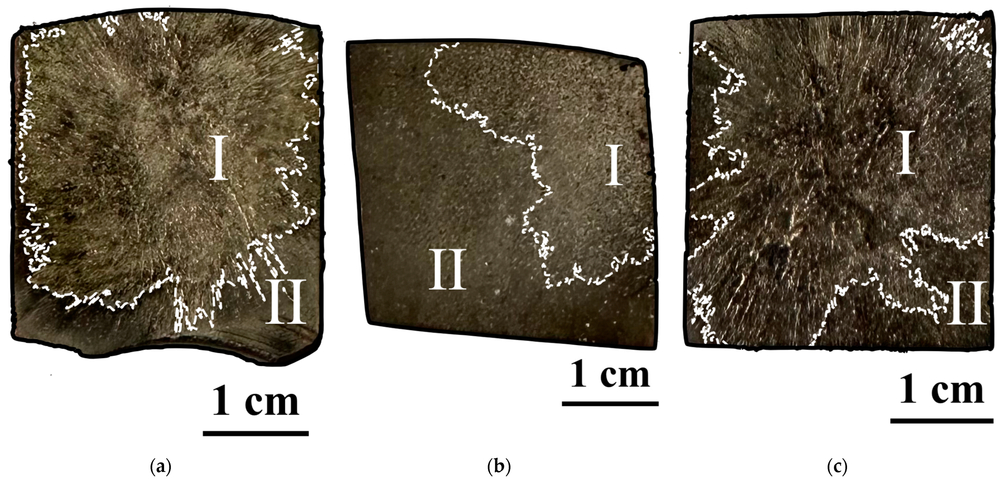
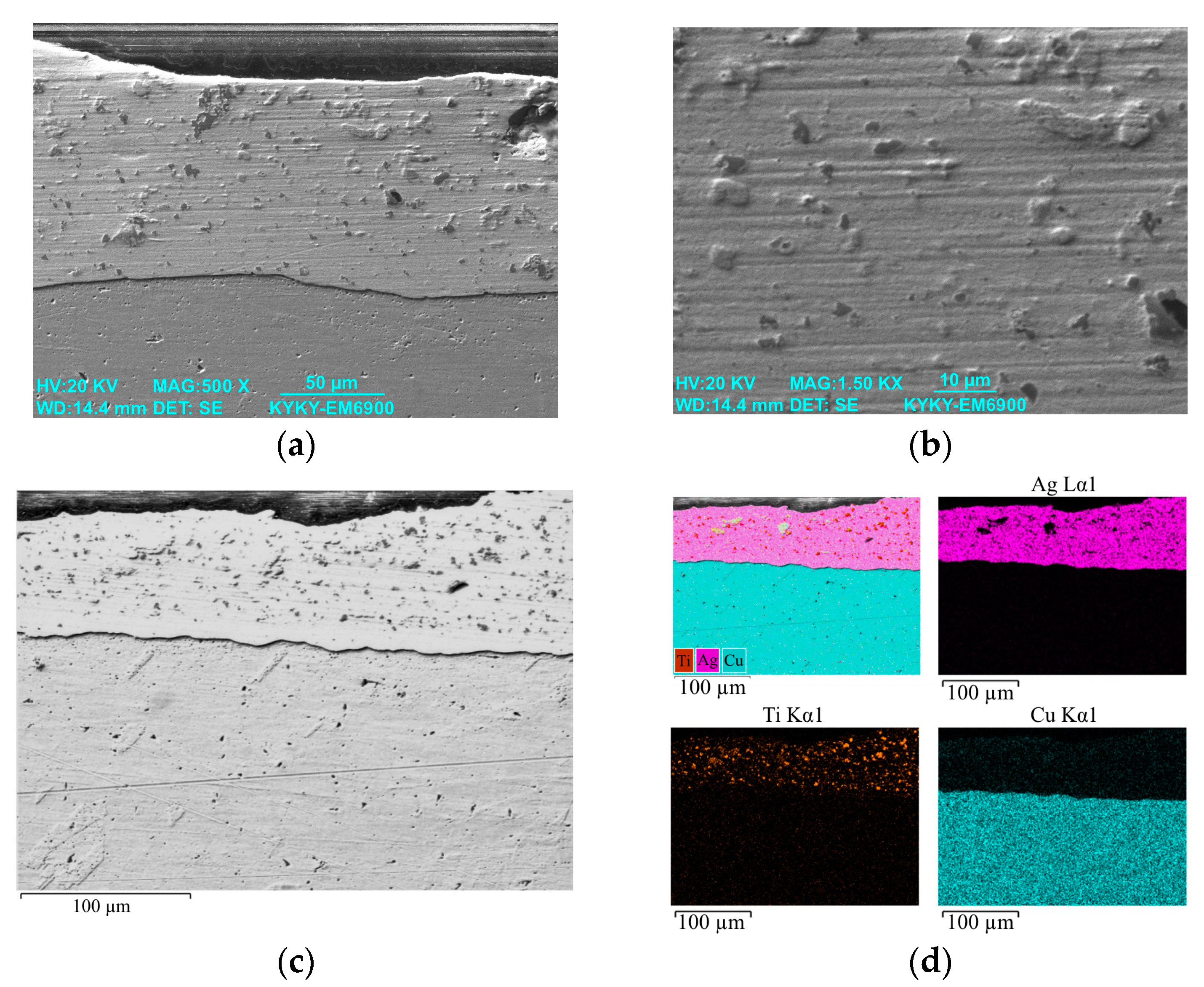
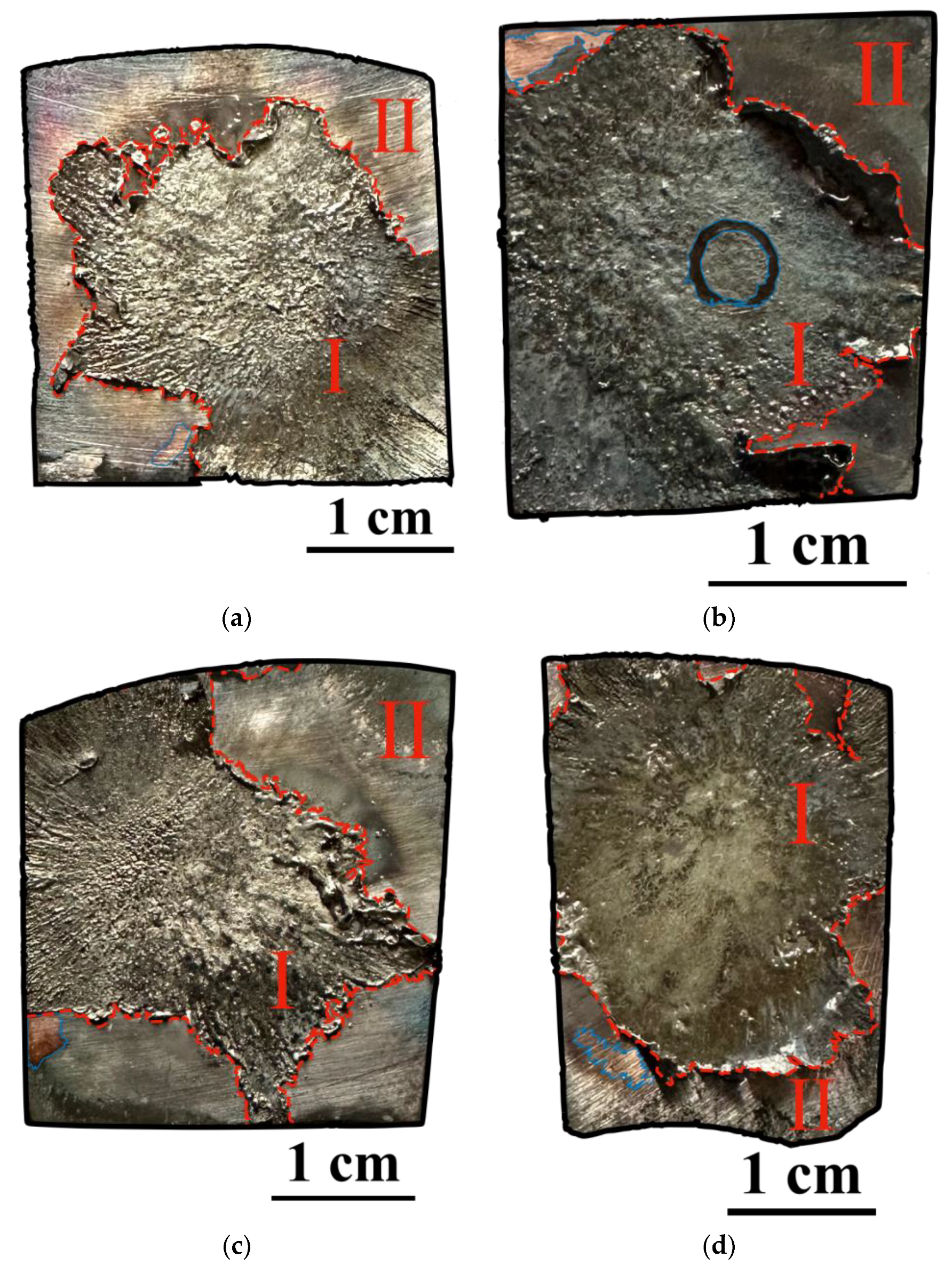
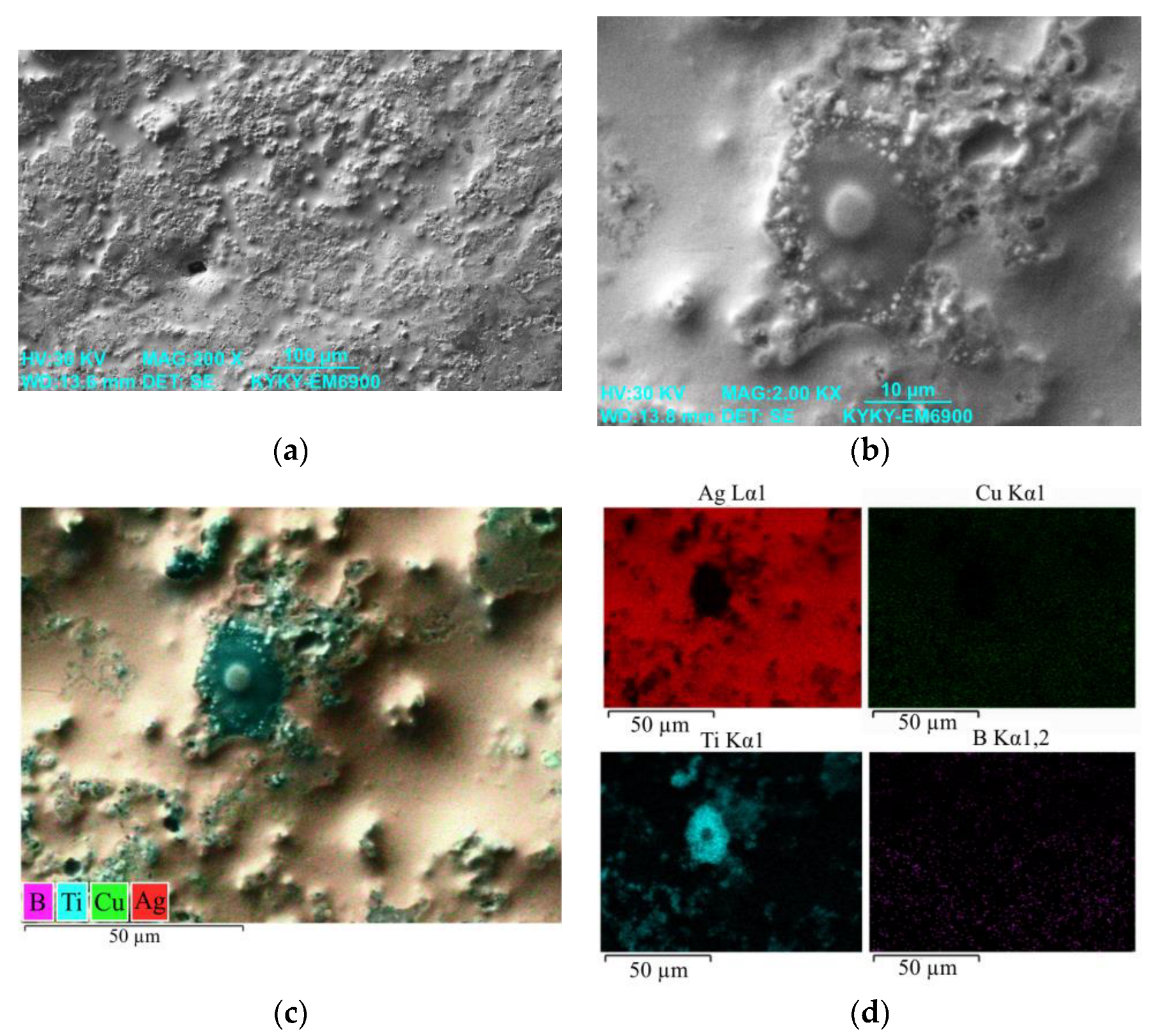
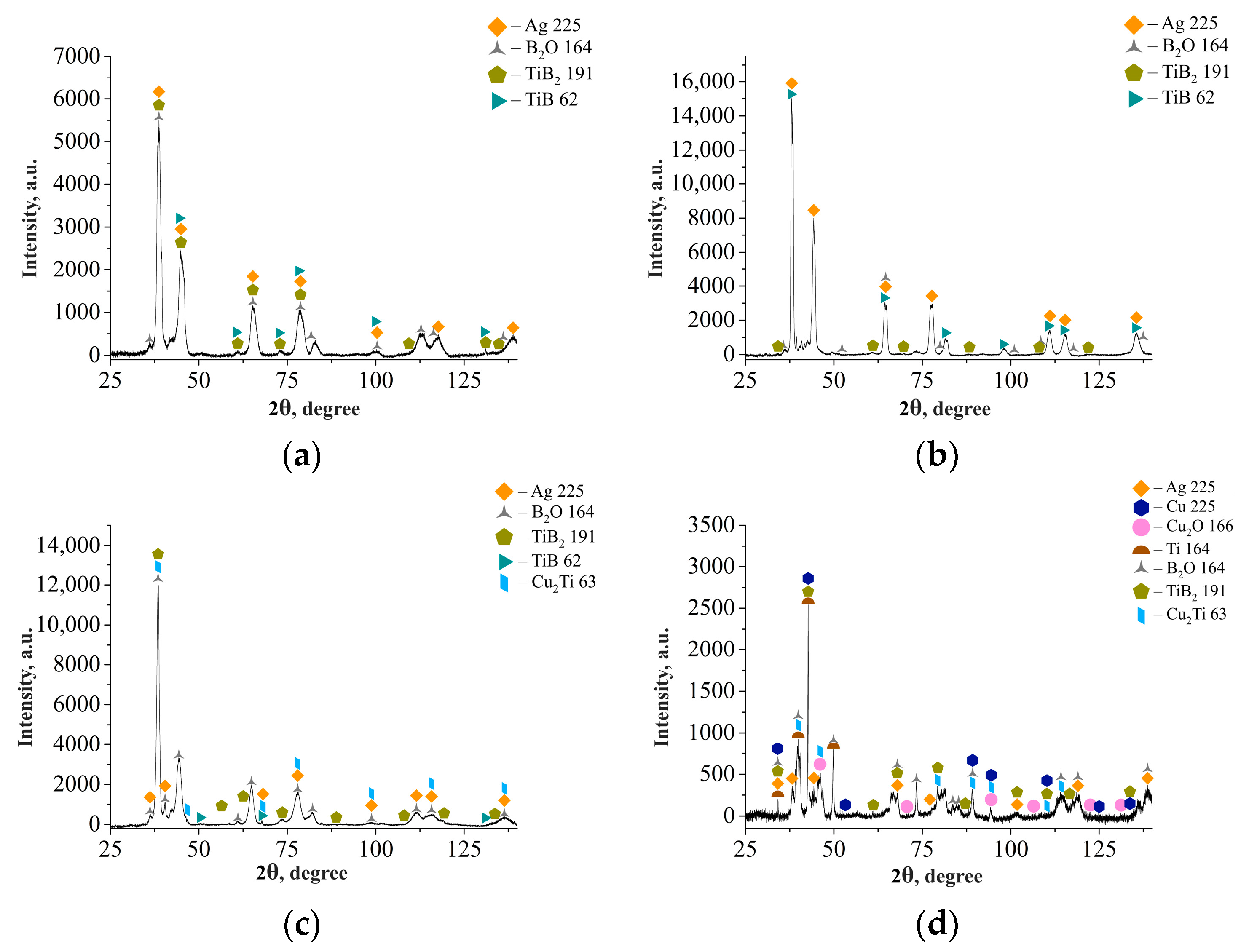
3.1. Study of the TiB2–Ag Coating Obtained by Electrical Explosion

Figure 3 shows the macro-characteristics of the three samples with electroexplosive coatings produced via the same spraying parameters. All coatings have a silver–grey color and different roughness. Visually, samples No. 1 and 3 differ significantly from sample No. 2. However, all samples had similar coating micromorphology. Visually, sample surfaces could be divided into two areas.
The area with droplet-like morphology (marked I in Figure 3) had over 65% of sample No. 1’s surface and over 85% of sample No. 3’s surface. The thin, long stripes of the melt flow traces could be observed in these areas near the boundaries. However, area I occupied less than 50% of sample No. 2’s surface. The flow traces were not found in sample No. 2. The impact of the coarse droplet component of the plasma jet formed area I.
The remaining part of the coating’s surface in all samples presented by the area (marked II in Figure 3) was formed by the impact of the vapor and fine droplet (<1 µm) component of the plasma jet.
Figure 4 shows the surface micro-morphology of area I of the coating sprayed by electrical explosion. The coating had multiscale roughness (Figure 4a). The base of the coating surface was formed by melt flow and hydrodynamic instabilities. Their size varied from 140 µm to millimeter size. Droplets and craters of different forms and shapes were randomly located on the surface. Their size varied from 3 µm to 50 µm (Figure 4b). The impact of nonmelted single TiB2 or silver conductor particles formed small droplets—big droplets formed from the fused agglomeration of silver and TiB2 particles (Figure 4c,d).
By surface EDS analysis (Figure 4d), copper traces were found on the coating’s surface. Copper atoms reached the coating’s surface due to discharge chamber (nozzle) surface ablation caused by the intense heat of the plasma jet.
Figure 5 illustrates the XRD patterns with the 10–140° diffraction angle range. XRD reflections corresponding to the Cu2O 224, Ag 166, TiB 216, Ag 225, Cu4Ti3 139, Cu 225, AgTi 129, B2O3 144, and B2O 164 phases were found in different samples. The phase composition was different for every sample. However, it is possible to find distinct phases in the pair of samples, as shown in Figure 6.
Due to nonequilibrium conditions of coating processing, two copper oxides with the same crystal lattice but different unit cell parameters formed in sample No. 1. It should be noted that the obtained phase parameters are significantly different from the reference values.
The oxide copper phase was also found in sample No. 2. Moreover, there was a substrate copper phase.
The phase composition of sample No. 3 was significantly different. There were no copper or copper-containing phases. The largest mass fraction belonged to B2O3 144. TiB2 may decompose at temperatures over 2000 °C [25]. TiB2 undergoes thermal decomposition into Ti and B because the temperature exceeds 3000 °C during electrical explosion spraying. B could be oxidized to B2O3, B2O because of the presence of air at 100 Pa in the discharge chamber.
Figure 7 illustrates the cross-sectional microstructures and EDS of the TiB2–Ag coating sprayed by electrical explosion. The thickness of the coating is about 100 µm. It can be seen that the TiB2 particles are uniformly dispersed in the Ag matrix. The average size of the particles ranges from 3.64 to 3.44 µm. The size of the inclusions was similar to the powder size. Groups of particles in amounts from two to five fused and formed big inclusions with sizes 10–15 µm. Agglomeration of particles consisting of groups of big inclusions or groups of over 15 particles forms clusters with an average size of more than 30 µm. Small pore sizes of the particles occur due to spalling TiB2 particles during cross-section preparation.
The coating matrix microstructure is shown in Figure 8a. There is a porous structure with a size of approximately 0.36 µm. Pores formed under non-equilibrium solidification form plenty of adsorbates, which exist on the substrate surface because of the low preheating temperature, and the low surface tension of droplets was caused by high droplet temperature [26,27]. Some pores consolidated in bigger pores with a size of ~2 µm in the areas with decreased gas solubility and cooling rate. Big holes form from the consolidation of such pores. The obtained microstructure is similar to the CuO–Ag coating microstructure previously achieved by the same method [28].
During plasma exposure, the melting front propagated into the volume of the metal simultaneously with the radial spreading of plasma along the surface, which led to a flow of the upper layers of the melt. Kelvin–Helmholtz instability occurred because of the speed difference between the melted substrate and moving plasma. As a result, the fluid-mechanically mixed layer was formed on the boundary between coating and substrate after solidification, as shown in Figure 9a. This layer may provide an important contribution to adhesive bonding.
The cracks appeared on the copper grain boundaries in the substrate, as shown in Figure 9a. Copper substrate cracking occurred because of the shock impact of the supersonic plasma jet on the grain boundary. Brittle copper oxide inclusion became the source of the microcracks. During cooling, microcracks grow under normal tensile stresses.
Figure 10 shows the TEM bright-field images and corresponding EDS results of the coating layer located at a 200–1000 nm distance from the surface. The coating morphology mainly comprises a matrix of layers ranging from approximately 450 nm to 600 nm thick and contains particles with melted boundaries. The EDS pattern of the particle in Figure 10b reveals that the particle is composed of elements Ti and B, so the particle is the reinforcement phase of TiB2. The main element of the matrix is silver. However, Ti stripes were also found in layers I and II and B atoms’ concentration increased in layer III. This indicates that TiB2 can both remain stable in the silver matrix and react with silver to form new compounds during electrical explosion spraying.
The spraying method instability characterizes the instability in phase composition and surface characteristics. In the process of electrical explosion spraying, the conductor consisting of foil and powder was heated and exploded, resulting in the ejection of different particles with different phases and sizes. These particles were accompanied by a shockwave generated by the explosion, forming a high-speed jet that impacted the substrate surface. The high-speed jet flow created by the explosion products under the influence of the shockwave generates a typical two-phase flow. Upon collision with the substrate, this flow dispersed in all directions, enveloping the substrate plane [29].
At the first stage of the spraying, heterogeneous plasma flux has two distinctive zones in the plasma accelerator: a high-speed jet with a low density and a high-density disk with a low speed. The effect on the target, typical for this procedure, is that the heat flow onto the surface has a nonmonotonic relation with time, that is, two maximums caused by time-separated influence by the central jet and the plasma flux. This circumstance furthers such effect of heat flows on the surface when plasma from the central electrode melts the surface, and plasma with particles of the ring disk saturates the melted metal of the bottom layer, causing, this way, modification of the top of the bottom layers and formation of unique gradient structures [30].
In that case, the initial location and form of the powder component on the foil affect the plasma flux formation and coating spraying result. For further studies, it is necessary to optimize the location and form of the powder component of the conductor.

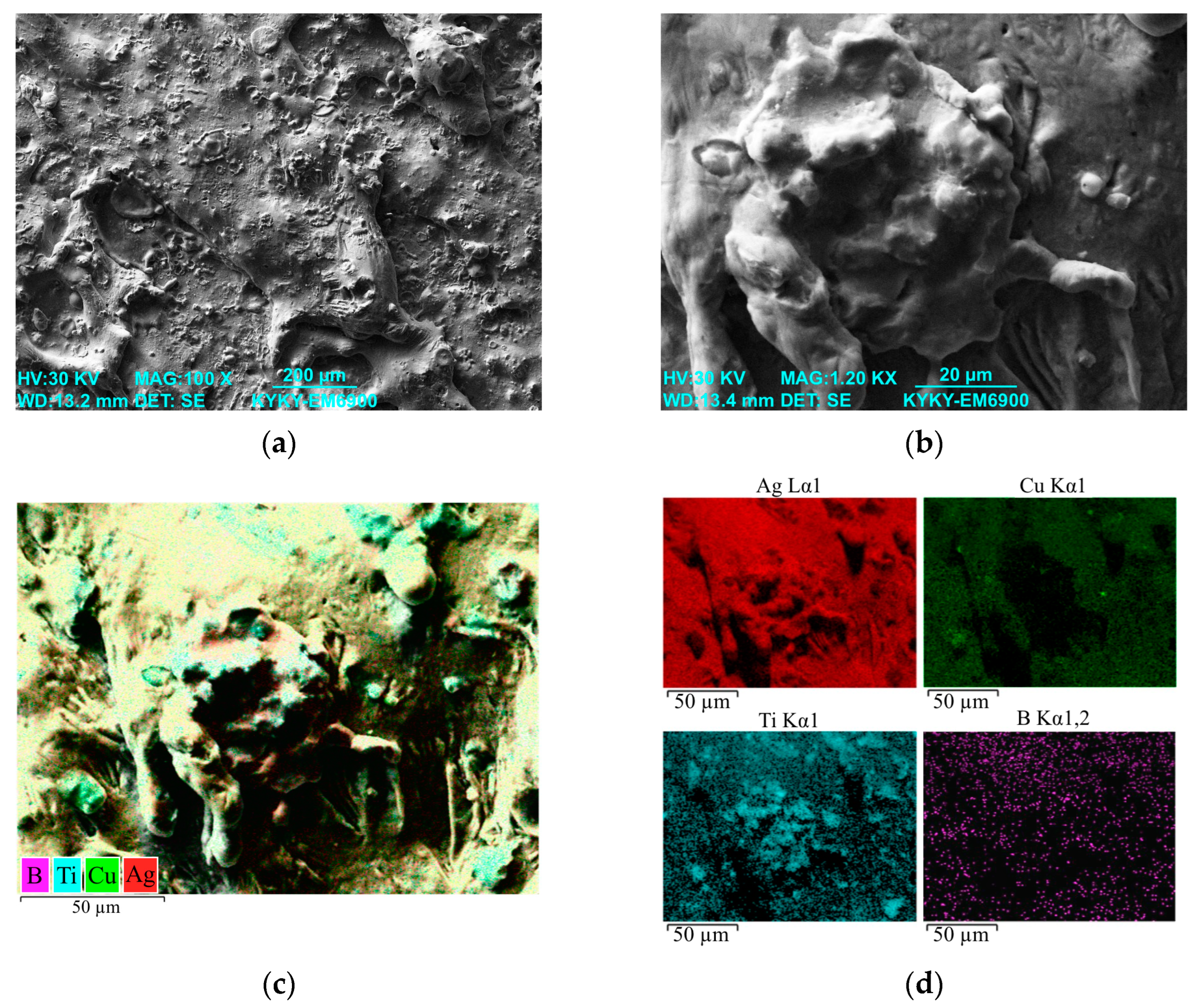
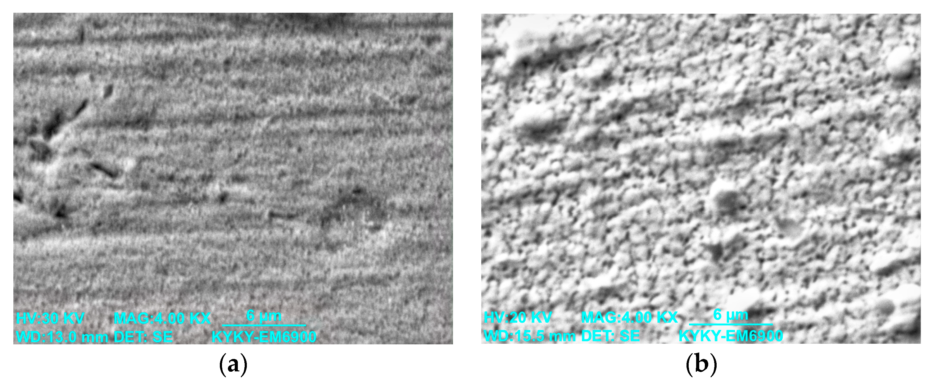
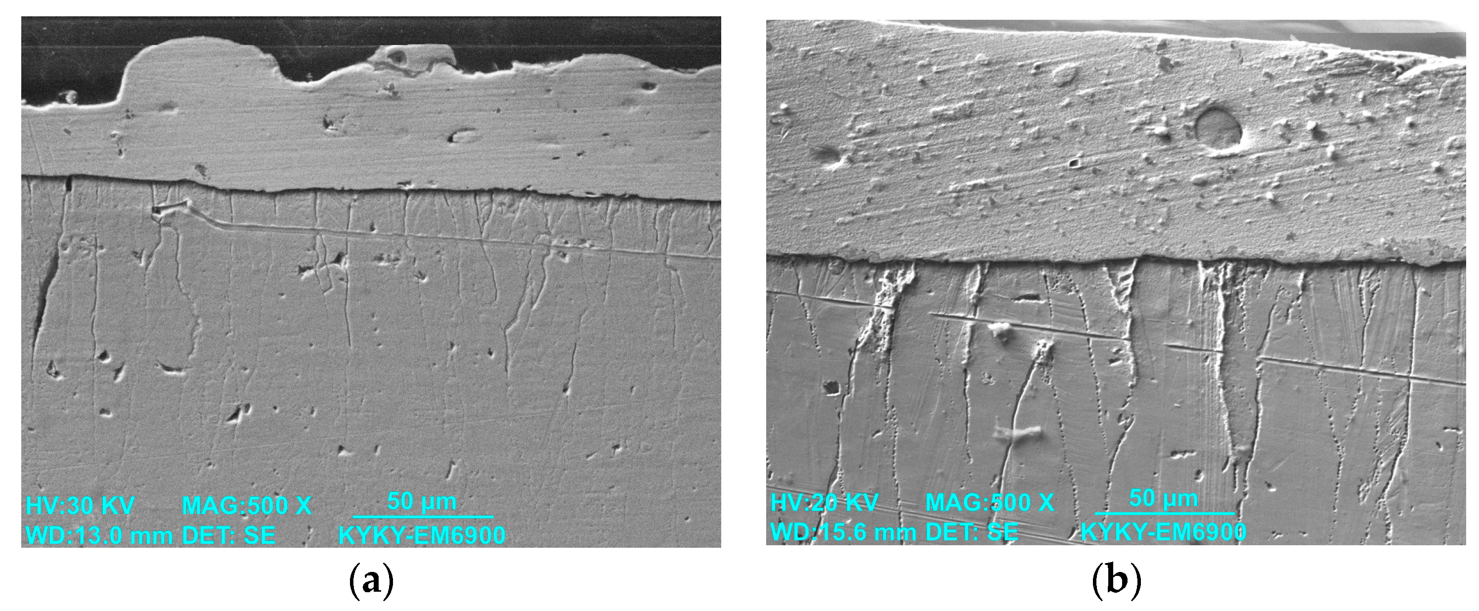
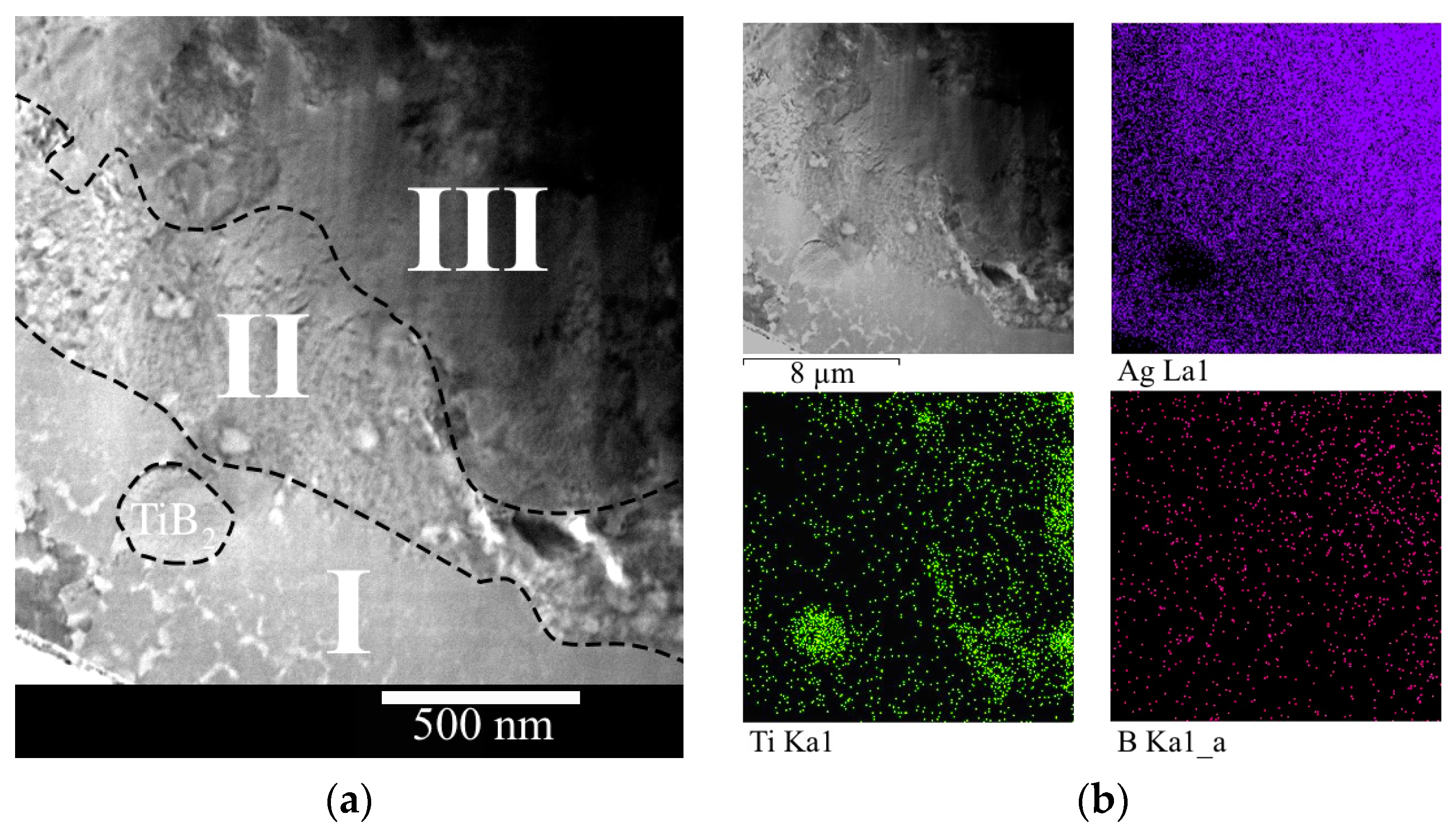
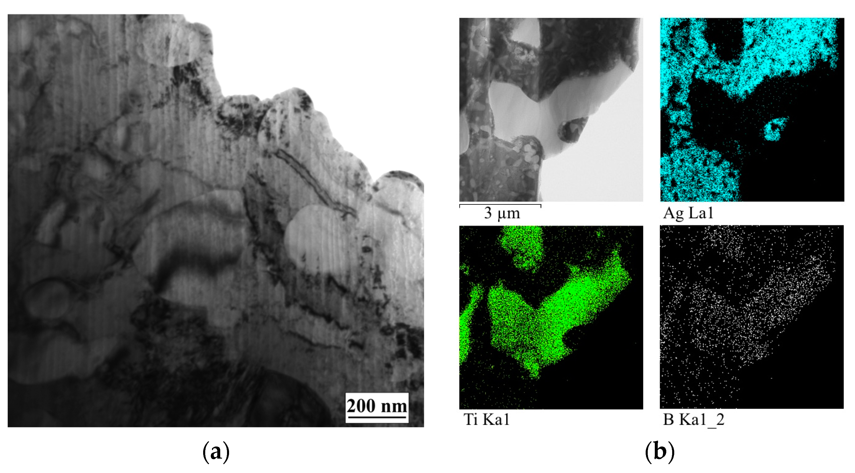
3.2. Study of the TiB2–Ag Coating Electron Beam Treatment Influence

The samples that were visually similar to those of No. 1 and 3 were selected for further electron beam treatment. The numbers of the applied electron beam treatment modes will be used to mark samples.
Figure 11 shows the macro-characteristics of the three samples after electron beam treatment. The coatings were significantly changed by electron beam treatment. Some parts of the coating peeled off and formed defective zones without coating. The central coating’s parts’ (area I) surfaces were smoothed. The droplet-like morphology was less visible. The edges of area I were bent. The peripheral parts of the coating (area II) became thinner. It is possible to see copper through these areas. However, some melt flow traces retained their shape.
Figure 12 shows the surface micro-morphology of the coating after electron beam treatment. Electron beam treatment rapidly heated coating material to the melting point, where there was rapid cooling by fast heat transfer into the deeper and cooler layers. Surface roughness is smoothed by surface tension forces in the liquid by vacuum. According to Figure 12c,d EDS element map images, there are many titanium inclusions on the surface with bubbles around them, forming groups and clusters. Some of them grew to the 15–20 µm size. Such a big titanium area could form from big droplets, shown in Figure 12b, by melting and evaporating low-melting silver and consolidation liquid TiB2 particles due to electron beam impact.
In order to explore the existing state of the elements after electron beam treatment, XRD was used to analyze the phase composition changes after electron beam treatment.
Figure 13 shows the XRD patterns of the samples after electron beam treatment. Phase composition changed. The TiB 62, Ag 225, Cu 225, Cu2O 166, Ti 164, B2O 164, TiB2 191, and Cu2Ti 63 phases were found in different samples.
It is clearly visible that increasing electron beam pulse energy and time led to the reduction in the Ag 225 phase. At the same time, the combined mass fraction of the TiB 62, Ti 164, B2O 164, and TiB2 191 refractory phases increases with electron beam pulse energy and time. There are copper-containing phases in samples No. 3 and 4, which may indicate that treatment regimes No. 3 and 4 lead to coating degeneration by evaporating the silver matrix, as shown in Figure 14.
The low-melt-point Ag 225 phase was evaporated by the electron beam impact. Reflexes between main silver peaks on the XRD patterns of sample No. 3 are more visible than in sample No. 1 but worse than in sample No. 2. The phase composition of sample No. 4 differs significantly compared to samples 1–3. The diffraction patterns of sample No. 4 contain wide silver reflections and narrow reflexes of the other phases.
Figure 15 illustrates the cross-sectional microstructures and corresponding EDS of the TiB2–Ag coating after electron beam treatment. It can be seen that coating thickness decreased by 12–14%. The coating structure was similar to samples without treatment. However, the number of clusters and big inclusion increased. Big holes were removed from the coating volume or significantly decreased in size. The average TiB2 particle size range decreased to 2.88–3.21 µm.
Cracks in the substrate formed by electrical explosion were filled with silver, as shown in Figure 9b. However, the possibility of cracks filling with silver should not be dismissed during electrical explosion spraying, as shown in the work of [31].
Figure 8b illustrates the cellular microstructure of the silver matrix after electron beam treatment. The small pores formed by electrical explosion spraying were removed and appeared as cellular structures. The cellular structure can be formed on the melt surface due to the developing capillary instability, which appeared because of the combination of thermocapillary, concentration and capillary, evaporation and capillary, and thermoelectric instabilities [32]. Previously, similar structures were found on the surface and surface layer of the irradiated aluminum alloys [33].
Figure 16 shows TEM images and an EDS element map. These images indicate that the TiB2–Ag coating layer located at a distance of 200 nm–23.5 µm from the surface after electron beam treatment consisted of a great amount of nanosized grains with different morphology, and the size ranged from tens of nanometers to hundreds of nanometers. Due to rapid cooling after electron beam treatment, the grains, thus, have little time to grow. The EDS results exhibit that both the grains contain Ag, Ti, and B. Dislocation lines were distributed around these grains. The high density of dislocations was evidenced. In addition to grains, fused TiB2 particles with an average size of approximately 1.5 µm were found.

4. Conclusions

The electron beam treatment of the TiB2–Ag coating deposited by an electrical explosion on the copper substrate was performed in four different regimes. The pulse energy density and duration varied during the different modes. All regimes changed the surface morphology. Microcraters, splats, and melt flow traces were removed from the surface and many titanium inclusions and bubbles appeared. The irregular phase composition of the sprayed TiB2–Ag coating was significantly changed by the electron beam treatment. Ag, TiB2, and B2O became the main phase in the modified coating. Increasing the pulse energy density and duration reduces the low-melting Ag phase and increases the mass fraction of the refractory phases B2O 164 and TiB2 191. Regimes No. 3 and No. 4 contributed to the formation of the copper-containing phases Cu 225, Cu2O 166, and Cu2Ti 63 due to the heating and melting of the copper substrate by the excess energy of the electron beam. The cross-sectional coating structure did not change significantly after electron beam treatment. There were silver matrix and TiB2 inclusions. The average TiB2 particle size decreased to 2.88–3.21 µm. The coating microstructure was transformed into a cellular crystallization structure due to the capillary instability caused by the electron beam treatment. The nanostructure of the modified samples consisted of a large number of nanosized grains with different morphologies and fused TiB2 particles.

Author Contributions

Conceptualization, D.A.R. and A.D.F.; validation, D.A.R. and V.V.P.; formal analysis, D.A.R., A.D.F., E.S.V. and V.V.P.; investigation, A.D.F., E.S.V. and V.V.P.; resources, D.A.R. and V.V.P.; writing—original draft preparation, D.A.R. and A.D.F.; visualization, A.D.F. and V.V.P.; project administration, D.A.R.; funding acquisition, D.A.R. All authors have read and agreed to the published version of the manuscript.

Funding

This research was funded by the Russian Science Foundation Grant No. 22-79-10012, https://rscf.ru/project/22-79-10012/ (accessed on 27 September 2023).

Institutional Review Board Statement

Not applicable.

Informed Consent Statement

Not applicable.

Data Availability Statement

The data presented in this study are available on request from the corresponding author.

Conflicts of Interest

The authors declare no conflict of interest. The funders had no role in the design of the study; in the collection, analyses, or interpretation of data; in the writing of the manuscript; or in the decision to publish the results.

References

  1. Grieseler, R.; Camargo, M.K.; Hopfeld, M.; Schmidt, U.; Bund, A.; Schaaf, P. Copper-MAX-Phase Composite Coatings Obtained by Electro-Co-Deposition: A Promising Material for Electrical Contacts. Surf. Coat. Technol. 2017, 321, 219–228. [Google Scholar] [CrossRef]
  2. Yang, F.; Wu, Y.; Rong, M.; Sun, H.; Murphy, A.B.; Ren, Z.; Niu, C. Low-Voltage Circuit Breaker Arcs—Simulation and Measurements. J. Phys. D Appl. Phys. 2013, 46, 273001. [Google Scholar] [CrossRef]
  3. Song, J.; Yuan, H.; Schinow, V. Fretting Corrosion Behavior of Electrical Contacts with Tin Coating in Atmosphere and Vacuum. Wear 2019, 426–427, 1439–1445. [Google Scholar] [CrossRef]
  4. Biyik, S.; Arslan, F.; Aydin, M. Arc-Erosion Behavior of Boric Oxide-Reinforced Silver-Based Electrical Contact Materials Produced by Mechanical Alloying. J. Electron. Mater. 2015, 44, 457–466. [Google Scholar] [CrossRef]
  5. Wu, C.; Zhao, Q.; Li, N.; Wang, H.; Yi, D.; Weng, W. Influence of Fabrication Technology on Arc Erosion of Ag/10SnO2 Electrical Contact Materials. J. Alloys Compd. 2018, 766, 161–177. [Google Scholar] [CrossRef]
  6. Zhou, Z.; Zhao, T.; Feng, Y.; Zhao, H.; Qian, G. Arc Erosion Characteristics Evolution of Ag/Ti3SiC2 Composites during Repetitive Arc Breakdowns in SF6 Gaseous Medium. Int. J. Appl. Ceram. Technol. 2021, 18, 1716–1724. [Google Scholar] [CrossRef]
  7. Ray, N.; Kempf, B.; Mützel, T.; Froyen, L.; Vanmeensel, K.; Vleugels, J. Effect of WC Particle Size and Ag Volume Fraction on Electrical Contact Resistance and Thermal Conductivity of Ag–WC Contact Materials. Mater. Des. 2015, 85, 412–422. [Google Scholar] [CrossRef]
  8. Kesim, M.T.; Yu, H.; Sun, Y.; Aindow, M.; Alpay, S.P. Corrosion, Oxidation, Erosion and Performance of Ag/W-Based Circuit Breaker Contacts: A Review. Corros. Sci. 2018, 135, 12–34. [Google Scholar] [CrossRef]
  9. Yangfang, C.; Xiaofang, Y.; Xiaoping, B.; Mingjiang, Z.; Jie, L.; Changlin, Y.; Xiufang, Z. Research on the Influence of Different Oxide Particles on Properties of AgCdO Contact Material. J. Phys. Conf. Ser. 2021, 1948, 012192. [Google Scholar] [CrossRef]
  10. Wang, X.; Yang, H.; Chen, M.; Zou, J.; Liang, S. Fabrication and Arc Erosion Behaviors of AgTiB2 Contact Materials. Powder Technol. 2014, 256, 20–24. [Google Scholar] [CrossRef]
  11. Nilsson, O.; Hauner, F.; Jeannot, D. Replacement of AgCdO by AgSnO/Sub2/ in DC Contactors. In Proceedings of the 50th IEEE Holm Conference on Electrical Contacts and the 22nd International Conference on Electrical Contacts Electrical Contacts, Seattle, WA, USA, 23–23 September 2004; pp. 70–74. [Google Scholar]
  12. Senthil, S.M.; Parameshwaran, R.; Rathanasamy, R.; Praveen Kumar, S. Fabrication of a Novel Silver-Based Electrical Contact Composites and Assessment of Its Mechanical and Electrical Properties. Arch. Metall. Mater. 2021, 66, 1087–1094. [Google Scholar]
  13. Ćosović, V.; Talijan, N.; Živković, D.; Minić, D.; Živković, Ž. Comparison of Properties of Silver-Metal Oxide Electrical Contact Materials. J. Min. Metall. Sect. B Metall. 2012, 48, 131–141. [Google Scholar] [CrossRef]
  14. Wang, X.; Li, G.; Zou, J.; Liang, S.; Fan, Z. Investigation on Preparation, Microstructure, and Properties of AgTiB2 Composite. J. Compos. Mater. 2011, 45, 1285–1293. [Google Scholar] [CrossRef]
  15. Li, H.; Wang, X.; Liu, Y.; Guo, X. Effect of Strengthening Phase on Material Transfer Behavior of Ag-Based Contact Materials under Different Voltages. Vacuum 2017, 135, 55–65. [Google Scholar] [CrossRef]
  16. Li, H.; Wang, X.; Guo, X.; Yang, X.; Liang, S. Material Transfer Behavior of AgTiB2 and AgSnO2 Electrical Contact Materials under Different Currents. Mater. Des. 2017, 114, 139–148. [Google Scholar] [CrossRef]
  17. Güler, O.; Varol, T.; Alver, Ü.; Biyik, S. The Wear and Arc Erosion Behavior of Novel Copper Based Functionally Graded Electrical Contact Materials Fabricated by Hot Pressing Assisted Electroless Plating. Adv. Powder Technol. 2021, 32, 2873–2890. [Google Scholar] [CrossRef]
  18. Güler, O.; Alver, Ü.; Varol, T. Fabrication and Characterization of Novel Layered Materials Produced by Electroless Plating and Hot Pressing. J. Alloys Compd. 2020, 835, 155278. [Google Scholar] [CrossRef]
  19. Güler, O.; Varol, T.; Alver, Ü.; Canakci, A. Effect of Al2O3 Content and Milling Time on the Properties of Silver Coated Cu Matrix Composites Fabricated by Electroless Plating and Hot Pressing. Mater. Today Commun. 2020, 24, 101153. [Google Scholar] [CrossRef]
  20. Wei, S.; Xu, B.; Wang, H.; Jin, G.; Lv, H. Comparison on Corrosion-Resistance Performance of Electro-Thermal Explosion Plasma Spraying FeAl-Based Coatings. Surf. Coat. Technol. 2007, 201, 5294–5297. [Google Scholar] [CrossRef]
  21. Tamura, H.; Konoue, M.; Sawaoka, A.B. Zirconium Boride and Tantalum Carbide Coatings Sprayed by Electrothermal Explosion of Powders. J. Therm. Spray Tech. 1997, 6, 463–468. [Google Scholar] [CrossRef]
  22. Koval’, N.N.; Ivanov, Y.F. Nanostructuring of Surfaces of Metalloceramic and Ceramic Materials by Electron-Beams. Russ. Phys. J. 2008, 51, 505–516. [Google Scholar] [CrossRef]
  23. Li, C.; Feng, J.; Yuan, W.; Cao, Y.; Han, R. Discharge Characteristics and Dynamic Process of Directional Spraying Binary and Ternary Alloy Coating via Electrical Explosion Method. In Proceedings of the 4th International Symposium on Plasma and Energy Conversion, Foshan, China, 14–16 October 2022; Dai, D., Zhang, C., Fang, Z., Lu, X., Eds.; Springer Nature: Singapore, 2023; pp. 302–311. [Google Scholar]
  24. Romanov, D.; Moskovskii, S.; Konovalov, S.; Sosnin, K.; Gromov, V.; Ivanov, Y. Improvement of Copper Alloy Properties in Electro-Explosive Spraying of ZnO-Ag Coatings Resistant to Electrical Erosion. J. Mater. Res. Technol. 2019, 8, 5515–5523. [Google Scholar] [CrossRef]
  25. Vlasova, M.; Kakazey, M.; Aguilar, P.A.M.; Tapia, R.G.; Reséndiz-González, M.C.; Hernandez, A.C.; Mel’nikov, I.V.; Fironov, Y. TiN–TiB2 Ceramics Degradation in the Region of a Steady-State Laser Heating. Surf. Coat. Technol. 2019, 378, 124738. [Google Scholar] [CrossRef]
  26. Ma, G.; Chen, S.; Wang, H. Impact Spread Behavior of Flying Droplets and Properties of Splats. In Micro Process and Quality Control of Plasma Spraying; Ma, G., Chen, S., Wang, H., Eds.; Springer Series in Advanced Manufacturing; Springer Nature: Singapore, 2022; pp. 87–202. ISBN 978-981-19274-2-3. [Google Scholar]
  27. Liu, Q.; Wang, Y.; Bai, Y.; Li, Z.D.; Tan, G.L.; Bao, M.Y.; Li, X.J.; Zhan, H.; Sun, Y.W.; Chong, N.J.; et al. Formation Mechanism of Gas Phase in Supersonic Atmospheric Plasma Sprayed NiCr-Cr3C2 Cermet Coatings. Surf. Coat. Technol. 2020, 397, 126052. [Google Scholar] [CrossRef]
  28. Romanov, D.A.; Moskovskii, S.V.; Glezer, A.M.; Gromov, V.E.; Sosnin, K.V. Phase Composition, Structure, and Wear Resistance of Electric-Explosive CuO–Ag System Coatings after Electron Beam Processing. Bull. Russ. Acad. Sci. Phys. 2019, 83, 1270–1274. [Google Scholar] [CrossRef]
  29. Wang, X.; Zhou, H.; Wei, Y.; Zhang, A.; Zhu, L. Electrical Explosion Spray of Ag/C Composite Coating and Its Deposition Behavior. Ceram. Int. 2022, 48, 4497–4504. [Google Scholar] [CrossRef]
  30. Sarychev, V.; Nevskii, S.; Konovalov, S.; Granovskii, A. Modeling of the Initial Stages of the Formation of Heterogeneous Plasma Flows in the Electric Explosion of Conductors. Curr. Appl. Phys. 2018, 18, 1101–1107. [Google Scholar] [CrossRef]
  31. Romanov, D.A.; Budovskikh, E.A.; Zhmakin, Y.D.; Gromov, V.E. Surface Modification by the EVU 60/10 Electroexplosive System. Steel Transl. 2011, 41, 464–468. [Google Scholar] [CrossRef]
  32. Nevskii, S.; Sarychev, V.; Konovalov, S.; Granovskii, A.; Gromov, V. Formation Mechanism of Micro- and Nanocrystalline Surface Layers in Titanium and Aluminum Alloys in Electron Beam Irradiation. Metals 2020, 10, 1399. [Google Scholar] [CrossRef]
  33. Sarychev, V.; Nevskii, S.; Konovalov, S.; Granovskii, A.; Ivanov, Y.; Gromov, V. Model of Nanostructure Formation in Al–Si Alloy at Electron Beam Treatment. Mater. Res. Express 2018, 6, 026540. [Google Scholar] [CrossRef]
Figure 1. Schematic diagram of the EVU 60/10 M plasma accelerator. 1—inner cylindrical electrode, 2—composite electrically exploded conductor, 3—insulating insert, 4—discharge chamber (nozzle), 5—treated sample holder, 6—outer ring electrode, 7—sprayed sample, 8—vacuum technological chamber.
Coatings 13 01867 g001
Figure 2. (a) A photo of the electrically exploded conductor used in the previous study. (b) A photo of the electrically exploded conductor of the new construction.
Coatings 13 01867 g002
Figure 3. The macro-characteristics of the TiB2–Ag coating sprayed by electrical explosion: (a) sample No. 1; (b) sample No. 2; (c) sample No. 3. The areas with droplet-like morphology are marked by I. The areas with fine morphology are marked by II. White dashed lines show borders between areas.
Coatings 13 01867 g003
Figure 4. SEM micrograph of the TiB2–Ag coating surface in area I: (a) the surface micro-morphology of the TiB2–Ag coating in area I; (b) SEM micrograph of the droplet on the TiB2–Ag coating surface; (c) merged EDS element map of the droplet; (d) EDS element map images of Ag, Cu, Ti, and B.
Coatings 13 01867 g004
Figure 5. XDR patterns of the electrical-explosion-sprayed TiB2–Ag coating on samples: (a) No. 1; (b) No. 2; (c) No. 3.
Coatings 13 01867 g005
Figure 6. Parameters of the phases formed in the TiB2–Ag coating obtained by electrical explosion: (a) mass fraction of phases; (b) CSR; (c) crystal lattice parameter a; (d) crystal lattice parameter c.
Coatings 13 01867 g006
Figure 7. SEM micrograph of (a,c) the electrical-explosion-sprayed TiB2–Ag coating and copper substrate cross-section morphology; (b) silver matrix with TiB2 inclusion morphology; (d) merged EDS element map of the TiB2–Ag coating and copper substrate cross-section and EDS element map images of Ag, Ti, and B.
Coatings 13 01867 g007
Figure 8. The SEM images of TiB2–Ag coating microstructure after (a) electrical explosion spraying and (b) electron beam treatment in mode No. 3.
Coatings 13 01867 g008
Figure 9. (a) Crack formation in the copper substrate after electrical explosion spraying; (b) silver matrix crack filling with silver matrix after electron beam treatment in regime No. 3.
Coatings 13 01867 g009
Figure 10. (a) TEM bright-field image of the TiB2–Ag coating layer located at a 200–1000 nm distance from the surface and (b) EDS element map images of Ag, Ti, and B. I, II and III indicate different layers in the TEM bright-field image.
Coatings 13 01867 g010
Figure 11. The macro-characteristics of the electrical-explosion-sprayed TiB2–Ag coating treated by electron beam: (a) sample No. 1; (b) sample No. 2; (c) sample No. 3; (d) sample No. 4. The areas formed on the areas with droplet-like morphology are marked by I. The areas formed on the areas with fine morphology are marked by II. Red dashed lines show borders between areas. Blue lines indicate defective zones without coating.
Coatings 13 01867 g011
Figure 12. SEM micrograph of the TiB2–Ag coating surface in area I after electron beam treatment: (a) the surface micro-morphology of the TiB2–Ag coating in area I after electron beam treatment; (b) SEM micrograph of the remelted titanium inclusion on TiB2–Ag coating surface; (c) merged EDS element map of the remelted titanium inclusion area; (d) EDS element map images of Ag, Cu, Ti, and B.
Coatings 13 01867 g012
Figure 13. XDR patterns of the TiB2–Ag coating treated by modes (a) No. 1, (b) No. 2, (c) No. 3, and (d) No. 4 of electron beam treatment.
Coatings 13 01867 g013
Figure 14. Parameters of the phases formed in the TiB2–Ag coating after electron beam treatment: (a) mass fraction of phases; (b) CSR; (c) crystal lattice parameter a; (d) crystal lattice parameter b; (e) crystal lattice parameter c.
Coatings 13 01867 g014
Figure 15. SEM micrograph of (a,c) the TiB2–Ag coating treated by the electron beam in mode No. 2 and copper substrate cross-section morphology (b) silver matrix with TiB2 cluster in silver matrix; (b) SEM micrograph of the droplet on the TiB2–Ag coating surface; (c) merged EDS element map of the TiB2–Ag coating and copper substrate cross-section and (d) EDS element map images of Ag, Ti, and B.
Coatings 13 01867 g015
Figure 16. (a) TEM bright-field image of the TiB2–Ag coating layer located at a distance of 200 nm–23.5 µm from the surface after electron beam treatment and (b) EDS element map images of Ag, Ti, and B.
Coatings 13 01867 g016
Table 1. Electron beam treatment modes.
Regime, NoPulse Energy Density, J/cm2Pulse Duration, µsNumber of PulsesPulse Frequency, s−1
14550300.3
250200300.3
360200300.3
470200300.3
Disclaimer/Publisher’s Note: The statements, opinions and data contained in all publications are solely those of the individual author(s) and contributor(s) and not of MDPI and/or the editor(s). MDPI and/or the editor(s) disclaim responsibility for any injury to people or property resulting from any ideas, methods, instructions or products referred to in the content.

