
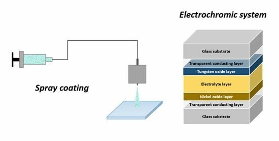
Film Deposition of Electrochromic Metal Oxides through Spray Coating: A Descriptive Review

Abstract
:
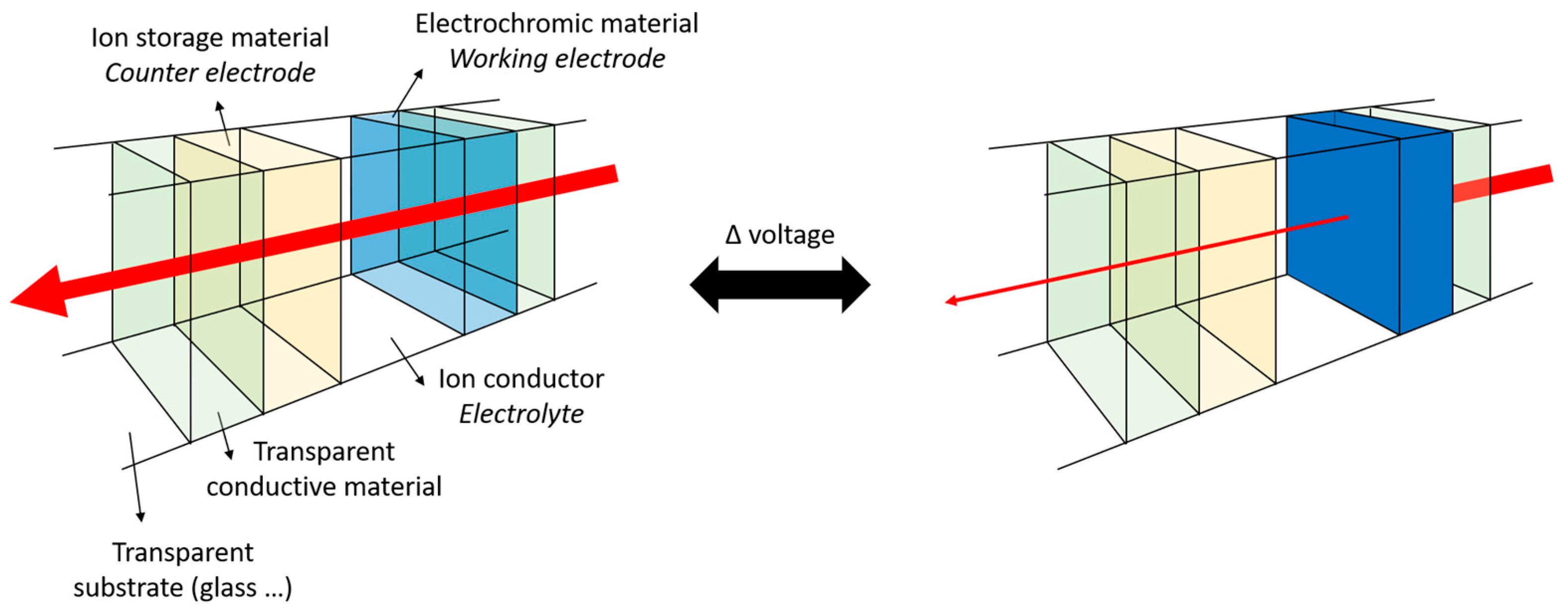
1. Electrochromism: Materials, Properties, and Fabrication Methods
- the optical contrast (i.e., the degree of transmittance modification ΔT% between clear and dark states, recorded at a single wavelength or within a specific wavelength range);
- the solar AM 1.5 coverage or integrated solar transmittance, defined as Equation (3):with being the transmittance at λ wavelength and being the incident solar intensity in the AM1.5G spectrum;
- the apparent color (regularly quantified in terms of coordinates from the International Commission on Illumination CIE color space with specific chromaticity plots) as well as the Haze factor (defined as the ratio between diffuse and total transmittances, which should be <2% to avoid an undesirable, milky, and troubling aspect in the smart window device);
- the switching speed or response time (the time required for a specific transmittance change, in terms of coloration tcol or bleaching tble, routinely equal to 90% of its full commutation run);
- the coloration efficiency CE, expressed in cm2/C, as the change in optical density OD at a defined wavelength induced by every unit of charge density Q inserted or extracted per unit area, i.e., Equation (4):
- the memory effect (i.e., the capacity to maintain a transmittance state without applying an additional charge);
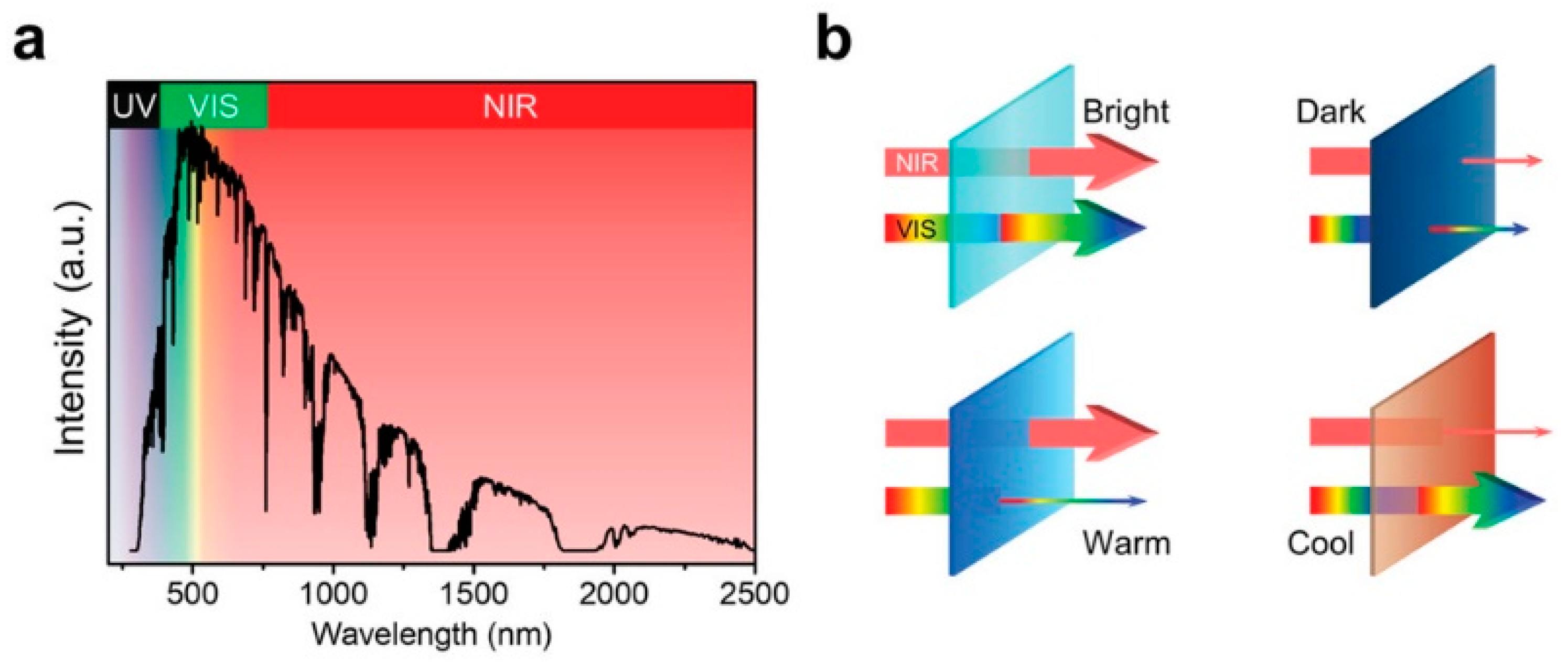
- the spectral selectivity (i.e., the ability to selectively control different wavelength ranges of transmittance, typically NIR independently of VIS);
- and the cycling stability and durability, characterized by the number of switching cycles during which the optical change can be preserved without significant degradation, being influenced by cycling testing conditions—the bias type and duration, electrolyte nature, temperature and pressure, illumination conditions, etc. To this end, the reader could refer to the recent report of J. Padilla et al. [40], presenting a detailed procedure that aims at adequately defining the testing conditions and the analytical description of the evolution of the performance of EC materials through continuous cycling. Their evaluation method relies on three steps: (i) define the reference switching conditions for each material, (ii) define the testing conditions used during the stability test, and (iii) use an analytical description of the contrast vs. the cycling run, like the number of cycles corresponding to an 80% performance retention. Various stability assessments were performed on common EC compounds, including conducting polymers, metal oxides, metallo-supramolecular polymers, and viologens, under a variety of test conditions.
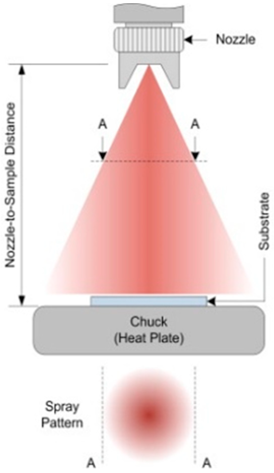
2. Spray Deposition: Principles and Methods
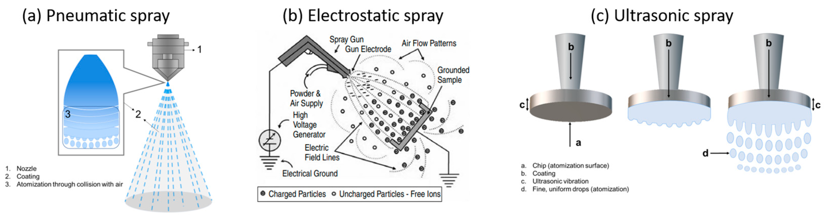
- Air or pneumatic spray (Figure 5a), in which compressed air is used to apply high pressure on the precursor fluid discharged from the nozzle, colliding at a high speed with the remaining air and then being split up and slowed down due to air resistance, before finally turning into a mist of droplets directed towards the target. Because they disperse a large quantity of precursor fluid, air spray setups can cause a significant excess of lost material, i.e., overspray.
- Electrostatic spray (Figure 5b), in which the precursor fluid is first charged with static electricity by applying a relatively high voltage within the spray nozzle (up to several thousands of V) and then changed into a droplet mist through electrostatic repulsion; the spray mist is then specifically attracted to the target surface standing on a grounded stage, therefore reducing the overspray quantity. Thanks to the strong electrical field in play, electrospray systems can be used with solutions and suspensions of quite high viscosities as well as with pastes and slurries.
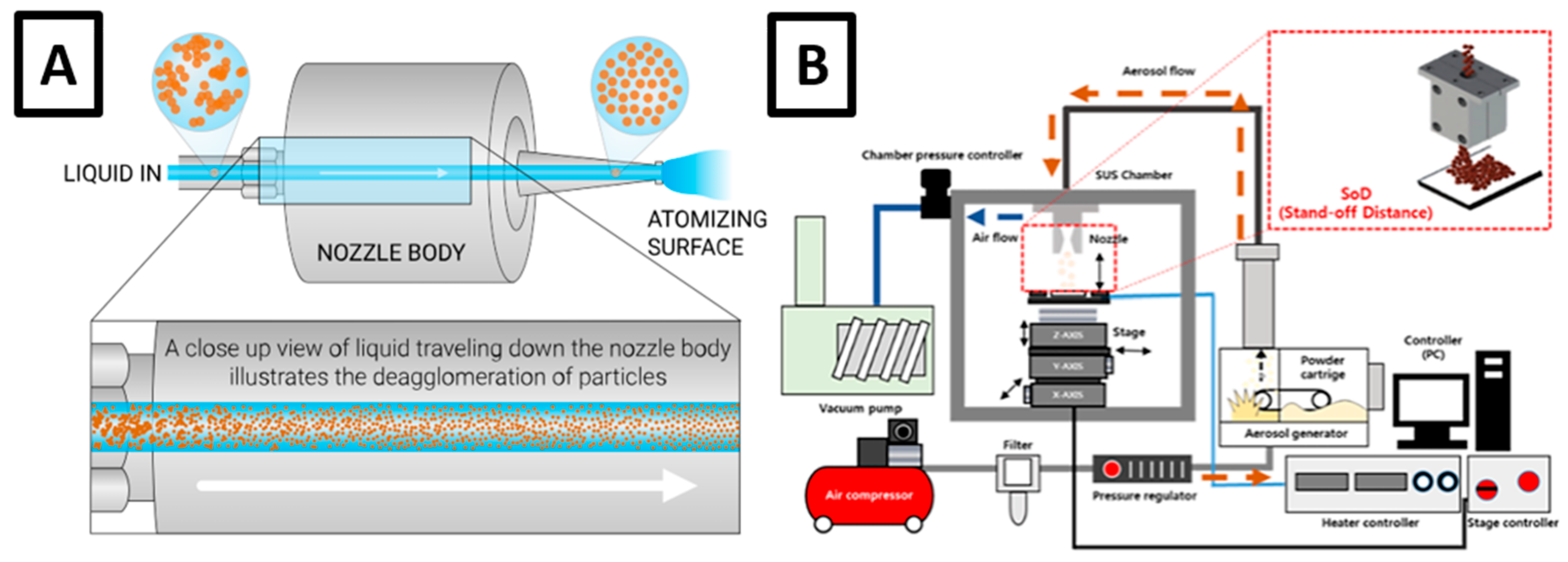
- Ultrasonic spray (Figure 5c), in which the nozzle is equipped with a chip (atomization surface) that vibrates upon ultrasonic waves, causing the precursor fluid to spread over the chip and ruffle; when the ultrasonic output becomes higher than the surface tension, the fluid is transformed into a fine droplet mist of a highly uniform size and size distribution (in comparison with other spray modes), being ultimately conveyed onto the substrate surface through a carrier gas of a passive (inert) or active (oxidative, reducing…) nature. By controlling the liquid flow and vibration frequency, ultrasonic spray has been shown to produce high-quality coatings with important uniformity, regular thickness, and strong adherence, also involving very limited overspray by producing almost no splashing or avoidable liquid spreading.
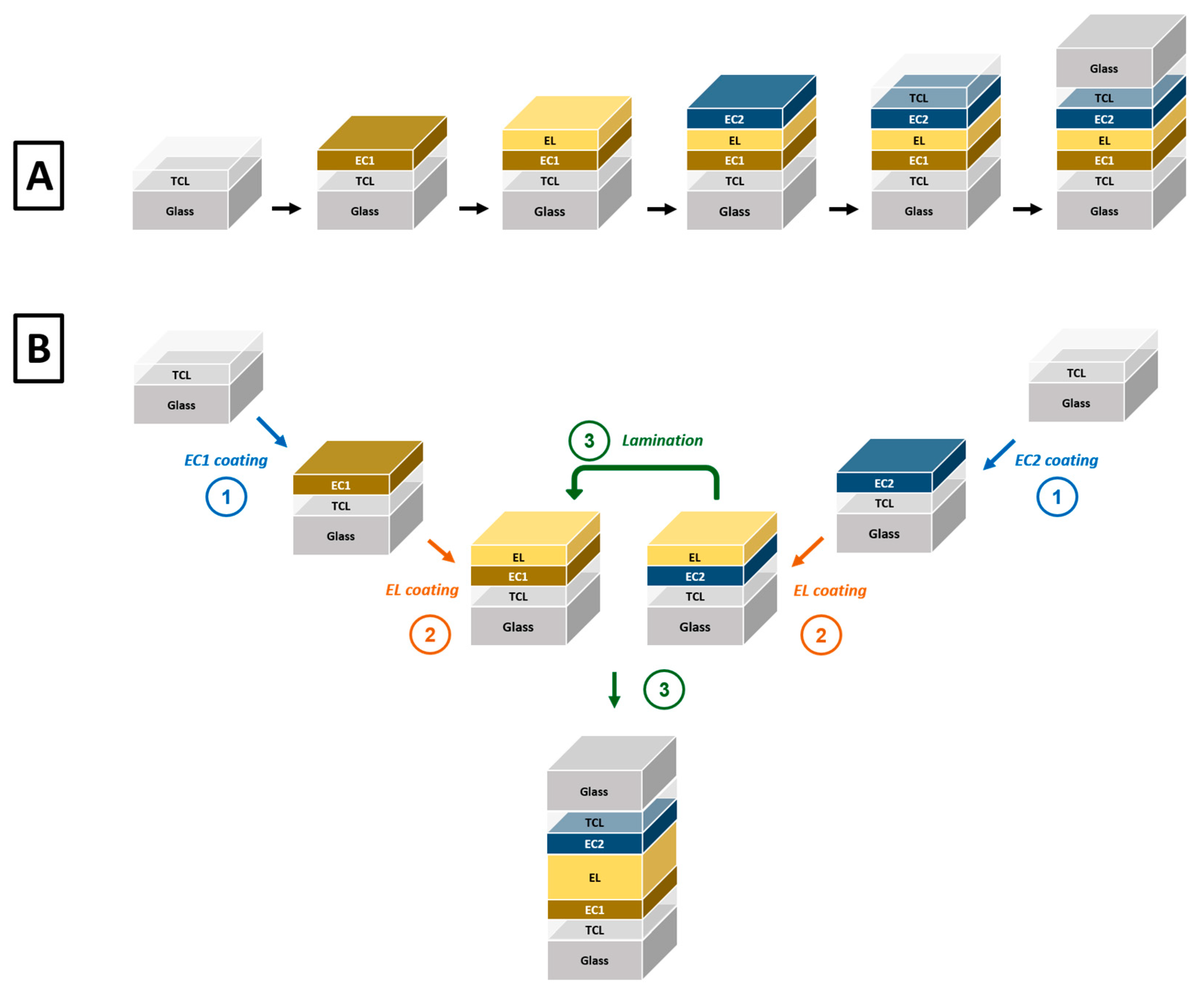
3. Spray Deposition of Electrochromic Metal Oxides
3.1. Tungsten Oxide WO3
3.2. Nickel Oxide NiO
3.3. Vanadium Pentoxide V2O5
3.4. Other Oxides
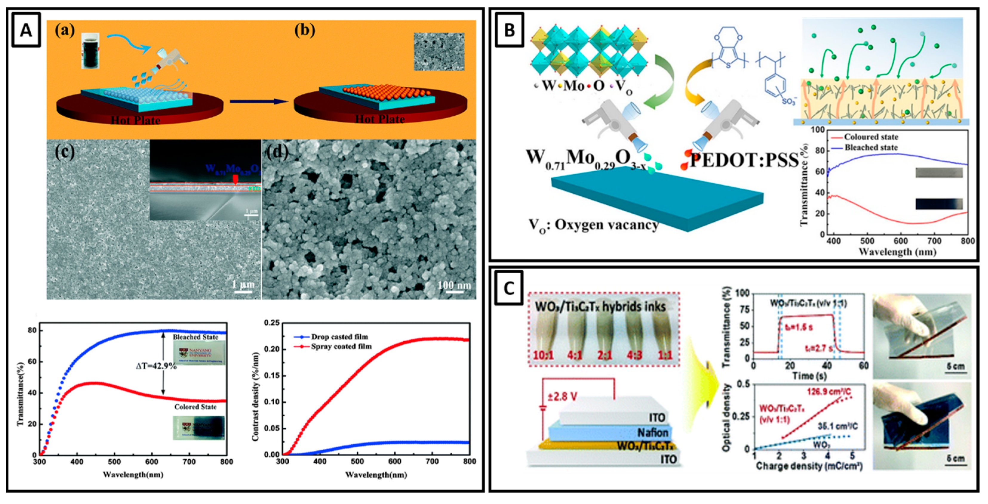
- MoO3, with works [187,188,189,190] reporting deposition protocols at high temperatures (250 to 400 °C), starting from precursor solutions constituting MoCl5 salts or MoO3 pre-formed powders and resulting in 100 to 550 nm thick layers with up to 23% of VIS optical contrast and 37 cm2/C of CE; further doping with W led to CE values improved up to 168 cm2/C [189].
- TiO2, obtained as 100 to 800 nm thick layers from titanium alkoxide precursors at spray temperatures of 200 to 680 °C and showing VIS ΔT values as high as 61%, a switching time below 10 s, and CEs of 18 to 101 cm2/C [191,192,193,194,195,196]; selected articles investigated the further doping of TiO2 with W [194], Nb [195], and Ni [196], the latter resulting in extremely high CE values of 474 cm2/C for 46% VIS ΔT. TiO2 layers can also be used as passive counter electrodes in assembled EC devices [191].
- Bi2O3, spray-processed at 500 °C from bismuth carbonate aqueous solutions, into 125–450 nm thick films presenting 71% optical contrast and 12–18 cm2/C [200].
- SnO2, for which P. Patil et al. explored various substrate temperatures between 450 and 500 °C for the pyrolytic transformation of tri-n-butyl tin acetate solutions into layers of 400–500 nm thickness [201]; a modest EC performance of 13% VIS optical contrast and 14 cm2/C of CE could be highlighted. In a later study, C.S. Lee and co-workers used pre-formed NPs of Sb-doped SnO2 (ATO) for NPDS-based spray coating at RT, leading to a ~35% VIS transmittance change and a CE of 16 cm2/C [61].

| Reference | Spray Conditions (Tdep for Deposition Temperature, t.t. for Thermal Treatment) | Thickness (nm) | Tble (%) | Tcol (%) | ΔT (%) | tble (s) | tcol (s) | CE (cm2/C) | Cycling Runs |
|---|---|---|---|---|---|---|---|---|---|
| MoO3 | |||||||||
| Patil [187] | MoO3 powder in NH4OH Tdep = 350 °C | 1100 | N.p. | N.p. | N.p. | N.p. | N.p. | N.p. | N.p. |
| Patil [188] | MoO3 powder in NH4OH and TiAcAc; Tdep = 350 °C | 130–540 | 47 | 31 | 16 | N.p. | N.p. | 19–37 | 1000 |
| Sahay [189] | MoCl5 + ammonium tungstate in methanol; Tdep = 390 °C | N.p. | 5–25 | 2–17 | 3–8 | 1–5 | 1–25+ | 35–168 | 100 |
| Unalan [190] | MoCl5 in H2O Tdep = 300 °C | 100–200 | 42–49 | 21–34 | 15–23 | N.p. | N.p. | 16–32 | 20 |
| TiO2 | |||||||||
| Patil [191] | TiAcAc in methanol Tdep = 350–450 °C | 200–400 | 65–85 | 50–80 | 5–10 | 3–4 | 4–5 | 3–4 | N.p. |
| Sivakumar [192] | Titanium isopropoxide in acetylacetone Tdep = 200–350 °C with t.t. at 450 °C | 800–1300 | 59–88 | 27–37 | 32–61 | 2 | 3 | 22–101 | 100 |
| Eshghi [193] | Titanium isopropoxide in ethanol and acetylacetone Tdep = 200 °C with t.t. at 450 °C | 300 | 90–95 | 45–75 | 17–53 | < 1 | 1–2 | 18–92 | N.p. |
| Zelazowska [194] | TiAcAc (and WAcAc) in dichloromethane and acetylacetone; Tdep = 680 °C | 110 | 70 | 15–30 | 40–55 | N.p. | N.p. | N.p. | N.p. |
| Zhao [195] | Ti(C4H9O)4 + NbCl5 in acetylacetone and ethanol; Tdep = 320–480 °C | 100–400 | 60–76 | 30–69 | 4–26 | 8–21 | 35–59 | N.p. | 1000 |
| Sivakumar [196] | Titanium isopropoxide and Ni acetate in ethanol and glycerol Tdep = 200 °C with t.t. at 450 °C | 350–600 | 68–89 | 22–61 | 28–46 | 2 | 2–3 | 123–474 | 1000 |
| Nb2O5 | |||||||||
| Patil [197] | Nb2O5 powder in tartaric acid Tdep = 300–400 °C | 480 | 78 | 62 | 16 | 5 | 4 | 13 | 1000 |
| Patil [198] | Nb2O5 powder in tartaric acid Tdep = 400 °C with t.t. at 500 °C | 450–480 | 77–87 | 62–78 | 8–15 | 4–5 | 3–4 | 10–13 | N.p. |
| Romero [199] | NbCl5 in H2O and ethanol and acetic acid Tdep = 350–500 °C with t.t. at 500–900 °C | 100–450 | 65 | 25–60 | 5–40 | 6 | 10 | 4–26 | 20 |
| Bi2O3 | |||||||||
| Bao [200] | Bi carbonate in H2O Tdep = 500 °C with t.t. at 550 °C | 125–450 | 81 | 10 | 71 | N.p. | N.p. | 12–18 | 4 |
| SnO2 | |||||||||
| Patil [201] | (C4H9)3Sn(OOCCH3) in methanol Tdep = 450–500 °C | 400–500 | 78–85 | 68–83 | 2–13 | <1 | <1 | 8–14 | N.p. |
| C.S. Lee [61] | Sb-doped SnO2 NPs Tdep = RT (NPDS) | 800 | 72–78 | 37–54 | 24–43 | ~1 | ~5 | 15 | 10 |
| ITO | |||||||||
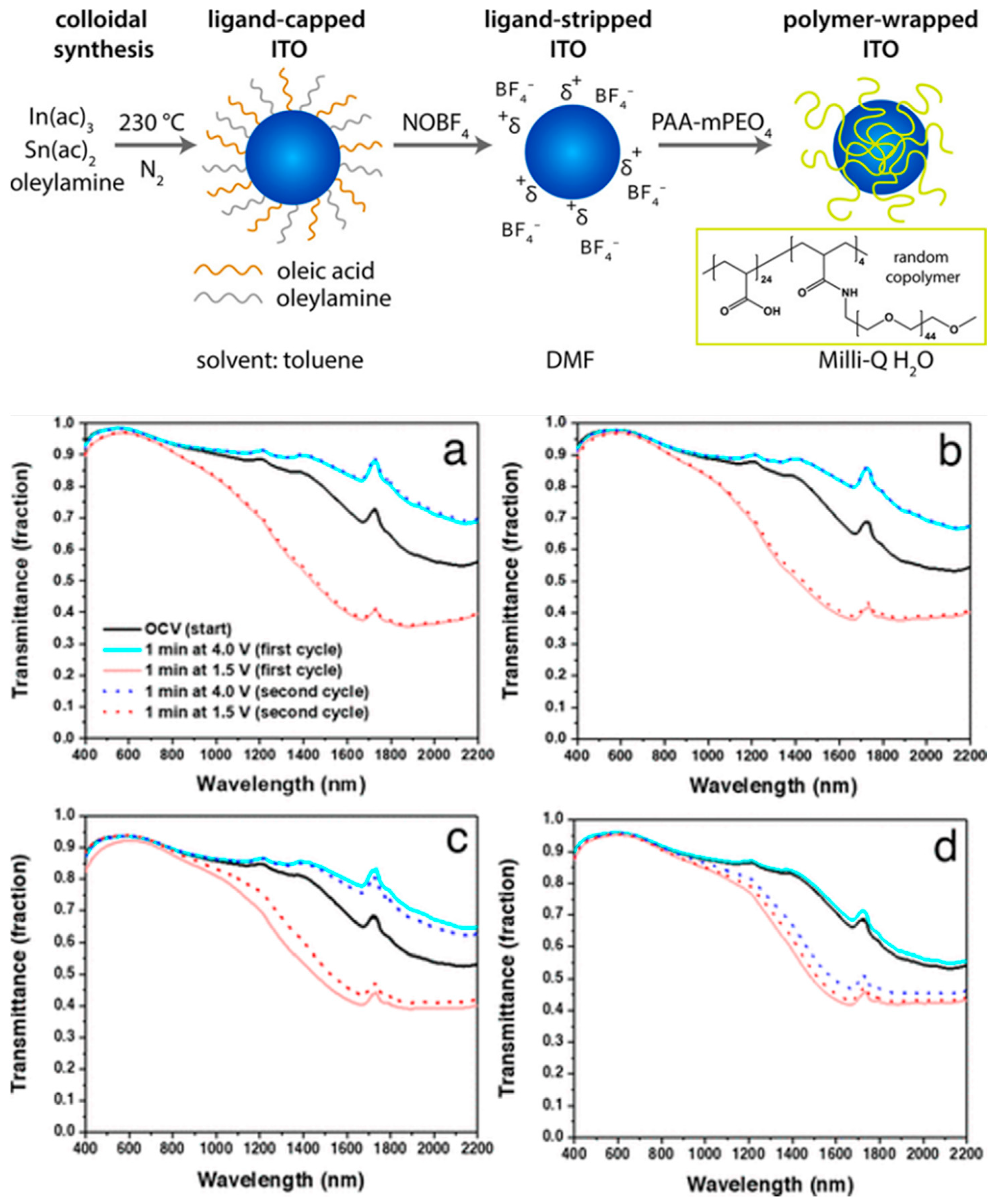
| Maho [202] | ITO NPs in isopropanol Tdep = RT with drying at 100 °C | 70–415 | 53–100 (in NIR) | 42–90 (in NIR) | 10–40 (in NIR) | N.p. | N.p. | N.p. | 10 |
| Maho [203] | ITO NPs in H2O Tdep = RT | 130 | 59–75 (in NIR) | 36–42 (in NIR) | 17–39 (in NIR) | N.p. | N.p. | 535–802 | N.p. |
| IrO2 | |||||||||
| Patil [204] | IrCl3 in H2O Tdep = 250–400 °C | 100–1200 | 25–60 | 20–52 | 2–30 | 2 | 5–6 | 10–26 | N.p. |
| Patil [205] | IrCl3 in H2O Tdep = 250 °C | 1200–3900 | 37–47 | 27–38 | 3–20 | 2–3 | 2–5 | 10–59 | N.p. |
| Hassanien [206] | IrCl3 in H2O Tdep = 250–520 °C with t.t. at 600 °C | 100–350 | N.p. | N.p. | N.p. | N.p. | N.p. | N.p. | N.p. |
| Mn3O4 | |||||||||
| Sivakumar [207] | MnCl2 in H2O Tdep = 350 °C | 940–1700 | N.p. | N.p. | 16–23 | N.p. | N.p. | 4–18 | 100 |
| Co3O4 | |||||||||
| Patil [208] | CoCl2 in H2O Tdep = 300 °C | 400 | 25 | 10 | 15 | 2 | 4 | N.p. | 1000 |
| Sivakumar [209] | Co(NO3)2 in H2O Tdep = 300–400 °C | 700–1000 | 14–95 | 10–66 | 4–29 | 1–2 | 1–3 | 1–12 | N.p. |
| Sivakumar [210] | Co(NO3)2·6H2O and Mn(CH3COO)2 in H2O Tdep = 400 °C | 685–850 | 19–61 | 9–26 | 6–35 | 1–4 | 2–3 | 10–29 | N.p. |
| Sivakumar [211] | Co(NO3)2 and Cr(NO3)2 in H2O Tdep = 400 °C | 680–785 | 29–45 | 7–32 | 8–38 | 2–4 | 2–3 | 3–47 | N.p. |
| El Bachiri [212] | CoCl2 in H2O Tdep = 350 °C | 500 | 40 | 10 | 31 | 2 | 4 | 19 | N.p. |
| CeO2 | |||||||||
| El Idrissi [217] | CeCl3 in H2O Tdep = 300–500 °C + t.t. at 300 °C | 300–800 | 80 (Tasdep) | N/A | N/A | N/A | N/A | N/A | 100 |
| Patil [218] | Ce(NO3)2 in methanol Tdep = 300–450 °C | 500–790 | 85 (Tasdep) | N/A | N/A | N/A | N/A | N/A | 600 |
| Patil [219] | Ce(NO3)2 + VCl3 in methanol Tdep not provided | N.p. | 68 | 62 | 6 | N.p. | N.p. | N.p. | N.p. |
| El Habib [220] | CeCl3 + VCl3 in H2O Tdep = 450 °C | N.p. | 50–65 (Tasdep) | N/A | <2 | N/A | N/A | N/A | 10 |
| Patil [221] | Ce(NO3)2·6H2O and Zr(NO3)2 in methanol Tdep = 400 °C | 540–600 | 86 (Tasdep) | N/A | N/A | <1 | N/A | N/A | 10000 |
| Patil [222] | Ce(NO3)3 and titanium isopropoxide in methanol; Tdep = 400 °C | N.p. | 75 (Tasdep) | 72 | 3 | N/A | N/A | N/A | 30000 |
4. Conclusions and Outcomes
Author Contributions
Funding
Institutional Review Board Statement
Informed Consent Statement
Data Availability Statement
Conflicts of Interest
List of Common Abbreviations (Alphabetic Order)
| AACVD | aerosol-assisted chemical vapor deposition |
| APCVD | atmospheric-pressure chemical vapor deposition |
| ATO | antimony-doped tin oxide |
| C | coulomb(s) |
| CE | coloration efficiency |
| CNTs | carbon nanotubes |
| CVD | chemical vapor deposition |
| DMF | N,N-dimethyl formamide |
| DC | direct current (sputtering) |
| EC | electrochromic |
| HTAB | hexadecyl trimetehyleammonium bromide |
| ITO | indium-tin oxide (or tin-doped indium oxide) |
| LSPR | localized surface plasmon resonance |
| MOFs | metal organic frameworks |
| NCs | nanocrystals |
| NIR | near-infrared |
| NPDS | nanoparticle deposition system |
| NPs | nanoparticles |
| OD | optical density |
| PANI | polyaniline |
| PEDOT:PSS | poly(3,4-ethylenedioxythiophene) polystyrene sulfonate |
| PEG | polyethylene glycol |
| PPy | polypyrrole |
| P123 | poly(ethylene glycol)-block-poly(propylene glycol)-block-poly(ethylene glycol) |
| P3HT | poly(3-hexylthiophene-2,5-diyl) |
| Q | charge density |
| RF | radio frequency (sputtering) |
| RT | room temperature |
| R&D | research and development |
| tcol | coloration time |
| tble | bleaching time |
| Tasdep | transmittance of as-deposited state |
| Tble | transmittance of bleached state |
| Tcol | transmittance of colored state |
| ΔT | contrast—difference in transmittance values of bleached and colored states |
| UV | ultraviolet |
| V | volt(s) |
| VIS | visible |
References
- Platt, J.R. Electrochromism, a Possible Change of Color Producible in Dyes by an Electric Field. J. Chem. Phys. 1961, 34, 862–863. [Google Scholar] [CrossRef]
- Deb, S.K. A Novel Electrophotographic System. Appl. Opt. 1969, 8, 192. [Google Scholar] [CrossRef]
- Deb, S.K. Optical and Photoelectric Properties and Colour Centres in Thin Films of Tungsten Oxide. Philos. Mag. 1973, 27, 801–822. [Google Scholar] [CrossRef]
- Lampert, C.M. Electrochromic Materials and Devices for Energy Efficient Windows. Sol. Energy Mater. 1984, 11, 1–27. [Google Scholar] [CrossRef]
- Svensson, J.S.E.M.; Granqvist, C.G. Electrochromic Coatings for “Smart Windows”. Sol. Energy Mater. 1985, 12, 391–402. [Google Scholar] [CrossRef]
- Mortimer, R.J.; Rosseinsky, D.R.; Monk, P.M.S. (Eds.) Electrochromic Materials and Devices, 1st ed.; Wiley: New York, NY, USA, 2013; ISBN 978-3-527-33610-4. [Google Scholar]
- Mortimer, R. Switching Colors with Electricity. Am. Sci. 2013, 101, 38. [Google Scholar] [CrossRef]
- Park, S.-I.; Quan, Y.-J.; Kim, S.-H.; Kim, H.; Kim, S.; Chun, D.-M.; Lee, C.S.; Taya, M.; Chu, W.-S.; Ahn, S.-H. A Review on Fabrication Processes for Electrochromic Devices. Int. J. Precis. Eng. Manuf.-Green Technol. 2016, 3, 397–421. [Google Scholar] [CrossRef]
- Wang, Y.; Runnerstrom, E.L.; Milliron, D.J. Switchable Materials for Smart Windows. Annu. Rev. Chem. Biomol. Eng. 2016, 7, 283–304. [Google Scholar] [CrossRef]
- Granqvist, C.G.; Arvizu, M.A.; Bayrak Pehlivan, İ.; Qu, H.-Y.; Wen, R.-T.; Niklasson, G.A. Electrochromic Materials and Devices for Energy Efficiency and Human Comfort in Buildings: A Critical Review. Electrochim. Acta 2018, 259, 1170–1182. [Google Scholar] [CrossRef]
- Shchegolkov, A.V.; Jang, S.-H.; Shchegolkov, A.V.; Rodionov, Y.V.; Sukhova, A.O.; Lipkin, M.S. A Brief Overview of Electrochromic Materials and Related Devices: A Nanostructured Materials Perspective. Nanomaterials 2021, 11, 2376. [Google Scholar] [CrossRef]
- Guo, J.; Liang, Y.; Zhang, S.; Ma, D.; Yang, T.; Zhang, W.; Li, H.; Cao, S.; Zou, B. Recent Progress in Improving Strategies of Metal Oxide-Based Electrochromic Smart Window. Green Energy Resour. 2023, 1, 100007. [Google Scholar] [CrossRef]
- Hopmann, E.; Zhang, W.; Li, H.; Elezzabi, A.Y. Advances in Electrochromic Device Technology through the Exploitation of Nanophotonic and Nanoplasmonic Effects. Nanophotonics 2023, 12, 637–657. [Google Scholar] [CrossRef] [PubMed]
- Zheng, J.Y.; Sun, Q.; Cui, J.; Yu, X.; Li, S.; Zhang, L.; Jiang, S.; Ma, W.; Ma, R. Review on Recent Progress in WO3-Based Electrochromic Films: Preparation Methods and Performance Enhancement Strategies. Nanoscale 2023, 15, 63–79. [Google Scholar] [CrossRef]
- Kandpal, S.; Ghosh, T.; Rani, C.; Chaudhary, A.; Park, J.; Lee, P.S.; Kumar, R. Multifunctional Electrochromic Devices for Energy Applications. ACS Energy Lett. 2023, 8, 1870–1886. [Google Scholar] [CrossRef]
- Gu, C.; Jia, A.-B.; Zhang, Y.-M.; Zhang, S.X.-A. Emerging Electrochromic Materials and Devices for Future Displays. Chem. Rev. 2022, 122, 14679–14721. [Google Scholar] [CrossRef]
- Beaujuge, P.M.; Reynolds, J.R. Color Control in π-Conjugated Organic Polymers for Use in Electrochromic Devices. Chem. Rev. 2010, 110, 268–320. [Google Scholar] [CrossRef]
- Österholm, A.M.; Nhon, L.; Shen, D.E.; Dejneka, A.M.; Tomlinson, A.L.; Reynolds, J.R. Conquering Residual Light Absorption in the Transmissive States of Organic Electrochromic Materials. Mater. Horiz. 2022, 9, 252–260. [Google Scholar] [CrossRef]
- Welsh, T.A.; Draper, E.R. Water Soluble Organic Electrochromic Materials. RSC Adv. 2021, 11, 5245–5264. [Google Scholar] [CrossRef]
- Liu, Q.; Yang, L.; Ling, W.; Guo, B.; Chen, L.; Wang, J.; Zhang, J.; Wang, W.; Mo, F. Organic Electrochromic Energy Storage Materials and Device Design. Front. Chem. 2022, 10, 1001425. [Google Scholar] [CrossRef]
- Granqvist, C.G. Electrochromics for Smart Windows: Oxide-Based Thin Films and Devices. Thin Solid Films 2014, 564, 1–38. [Google Scholar] [CrossRef]
- Patel, K.J.; Bhatt, G.G.; Ray, J.R.; Suryavanshi, P.; Panchal, C.J. All-Inorganic Solid-State Electrochromic Devices: A Review. J. Solid State Electrochem. 2017, 21, 337–347. [Google Scholar] [CrossRef]
- Xiong, S.; Yin, S.; Wang, Y.; Kong, Z.; Lan, J.; Zhang, R.; Gong, M.; Wu, B.; Chu, J.; Wang, X. Organic/Inorganic Electrochromic Nanocomposites with Various Interfacial Interactions: A Review. Mater. Sci. Eng. B 2017, 221, 41–53. [Google Scholar] [CrossRef]
- Tao, C.; Li, Y.; Wang, J. The Progress of Electrochromic Materials Based on Metal–Organic Frameworks. Coord. Chem. Rev. 2023, 475, 214891. [Google Scholar] [CrossRef]
- Lahav, M.; van der Boom, M.E. Polypyridyl Metallo-Organic Assemblies for Electrochromic Applications. Adv. Mater. 2018, 30, 1706641. [Google Scholar] [CrossRef]
- Ding, Y.; Wang, M.; Mei, Z.; Diao, X. Different Ion-Based Electrolytes for Electrochromic Devices: A Review. Sol. Energy Mater. Sol. Cells 2022, 248, 112037. [Google Scholar] [CrossRef]
- Eh, A.L.; Tan, A.W.M.; Cheng, X.; Magdassi, S.; Lee, P.S. Recent Advances in Flexible Electrochromic Devices: Prerequisites, Challenges, and Prospects. Energy Technol. 2018, 6, 33–45. [Google Scholar] [CrossRef]
- Yang, G.; Zhang, Y.-M.; Cai, Y.; Yang, B.; Gu, C.; Zhang, S.X.-A. Advances in Nanomaterials for Electrochromic Devices. Chem. Soc. Rev. 2020, 49, 8687–8720. [Google Scholar] [CrossRef]
- Rai, V.; Singh, R.S.; Blackwood, D.J.; Zhili, D. A Review on Recent Advances in Electrochromic Devices: A Material Approach. Adv. Eng. Mater. 2020, 22, 2000082. [Google Scholar] [CrossRef]
- Liang, Y.; Cao, S.; Guo, J.; Zeng, R.; Zhao, J.; Zou, B. Dual-Band Electrochromic Smart Window Based on Single-Component Nanocrystals. ACS Appl. Electron. Mater. 2022, 4, 5109–5118. [Google Scholar] [CrossRef]
- Tandon, B.; Lu, H.-C.; Milliron, D.J. Dual-Band Electrochromism: Plasmonic and Polaronic Mechanisms. J. Phys. Chem. C 2022, 126, 9228–9238. [Google Scholar] [CrossRef]
- Bai, T.; Li, W.; Fu, G.; Zhang, Q.; Zhou, K.; Wang, H. Dual-Band Electrochromic Smart Windows towards Building Energy Conservation. Sol. Energy Mater. Sol. Cells 2023, 256, 112320. [Google Scholar] [CrossRef]
- Zhai, Y.; Li, J.; Shen, S.; Zhu, Z.; Mao, S.; Xiao, X.; Zhu, C.; Tang, J.; Lu, X.; Chen, J. Recent Advances on Dual-Band Electrochromic Materials and Devices. Adv. Funct. Mater. 2022, 32, 2109848. [Google Scholar] [CrossRef]
- Gong, H.; Li, W.; Fu, G.; Zhang, Q.; Liu, J.; Jin, Y.; Wang, H. Recent Progress and Advances in Electrochromic Devices Exhibiting Infrared Modulation. J. Mater. Chem. A 2022, 10, 6269–6290. [Google Scholar] [CrossRef]
- Huang, L.; Cao, S.; Liang, Y.; Chen, J.; Yang, T.; Zhao, J.; Zou, B. Advances in multicolor electrochromic devices based on inorganic materials. J. Mater. Chem. C 2023, 11, 10107–10120. [Google Scholar] [CrossRef]
- Bian, C.; Wang, J.; Liu, H.; Yan, Y.; Zhang, P.; Yang, W.; Jia, S.; Guo, X.; Cai, G. Complementary multicolor electrochromic devices with excellent stability based on porous tin oxide nanosheet scaffold. Nano Res. 2023. [Google Scholar] [CrossRef]
- Runnerstrom, E.L.; Llordés, A.; Lounis, S.D.; Milliron, D.J. Nanostructured Electrochromic Smart Windows: Traditional Materials and NIR-Selective Plasmonic Nanocrystals. Chem. Commun. 2014, 50, 10555–10572. [Google Scholar] [CrossRef]
- Kriegel, I.; Scotognella, F.; Manna, L. Plasmonic Doped Semiconductor Nanocrystals: Properties, Fabrication, Applications and Perspectives. Phys. Rep. 2017, 674, 1–52. [Google Scholar] [CrossRef]
- Agrawal, A.; Cho, S.H.; Zandi, O.; Ghosh, S.; Johns, R.W.; Milliron, D.J. Localized Surface Plasmon Resonance in Semiconductor Nanocrystals. Chem. Rev. 2018, 118, 3121–3207. [Google Scholar] [CrossRef]
- Padilla, J.; Niklaus, L.; Schott, M.; Posset, U.; Faceira, B.; Mjejri, I.; Rougier, A.; Alesanco, Y.; Viñuales, A.; Shen, D.E.; et al. Quantitative Assessment of the Cycling Stability of Different Electrochromic Materials and Devices. ACS Appl. Opt. Mater. 2023, 1, 1174–1183. [Google Scholar] [CrossRef]
- Gesheva, K.; Ivanova, T.; Bodurov, G.; Szilágyi, I.M.; Justh, N.; Kéri, O.; Boyadjiev, S.; Nagy, D.; Aleksandrova, M. Technologies for Deposition of Transition Metal Oxide Thin Films: Application as Functional Layers in “Smart Windows” and Photocatalytic Systems. J. Phys. Conf. Ser. 2016, 682, 012011. [Google Scholar] [CrossRef]
- Wang, Z.; Kang, Y.; Zhao, S.; Zhu, J. Self-Limiting Assembly Approaches for Nanoadditive Manufacturing of Electronic Thin Films and Devices. Adv. Mater. 2020, 32, 1806480. [Google Scholar] [CrossRef]
- Ukoba, K.O.; Eloka-Eboka, A.C.; Inambao, F.L. Review of Nanostructured NiO Thin Film Deposition Using the Spray Pyrolysis Technique. Renew. Sustain. Energy Rev. 2018, 82, 2900–2915. [Google Scholar] [CrossRef]
- Rahemi Ardekani, S.; Sabour Rouh Aghdam, A.; Nazari, M.; Bayat, A.; Yazdani, E.; Saievar-Iranizad, E. A Comprehensive Review on Ultrasonic Spray Pyrolysis Technique: Mechanism, Main Parameters and Applications in Condensed Matter. J. Anal. Appl. Pyrolysis 2019, 141, 104631. [Google Scholar] [CrossRef]
- Li, X.; Perera, K.; He, J.; Gumyusenge, A.; Mei, J. Solution-Processable Electrochromic Materials and Devices: Roadblocks and Strategies towards Large-Scale Applications. J. Mater. Chem. C 2019, 7, 12761–12789. [Google Scholar] [CrossRef]
- Butt, M.A. Thin-Film Coating Methods: A Successful Marriage of High-Quality and Cost-Effectiveness—A Brief Exploration. Coatings 2022, 12, 1115. [Google Scholar] [CrossRef]
- Coating & Dispensing Technology—KEYENCE. Available online: https://www.keyence.com/ss/products/measure/sealing/coater-type/spray.jsp (accessed on 21 September 2023).
- Uniform Thin Film Layers of Functional Nanomaterials—Sono-Tek. Available online: https://www.sono-tek.com/industry/alternative-energy-nanomaterials/cnt-nanowires-and-other-nanomaterials/ (accessed on 21 September 2023).
- Abdellah, A.; Fabel, B.; Lugli, P.; Scarpa, G. Spray Deposition of Organic Semiconducting Thin-Films: Towards the Fabrication of Arbitrary Shaped Organic Electronic Devices. Org. Electron. 2010, 11, 1031–1038. [Google Scholar] [CrossRef]
- Wengeler, L.; Schmitt, M.; Peters, K.; Scharfer, P.; Schabel, W. Comparison of Large Scale Coating Techniques for Organic and Hybrid Films in Polymer Based Solar Cells. Chem. Eng. Process. Process Intensif. 2013, 68, 38–44. [Google Scholar] [CrossRef]
- Eslamian, M. Spray-on Thin Film PV Solar Cells: Advances, Potentials and Challenges. Coatings 2014, 4, 60–84. [Google Scholar] [CrossRef]
- Aziz, F.; Ismail, A.F. Spray Coating Methods for Polymer Solar Cells Fabrication: A Review. Mater. Sci. Semicond. Process. 2015, 39, 416–425. [Google Scholar] [CrossRef]
- Slegers, S.; Linzas, M.; Drijkoningen, J.; D’Haen, J.; Reddy, N.; Deferme, W. Surface Roughness Reduction of Additive Manufactured Products by Applying a Functional Coating Using Ultrasonic Spray Coating. Coatings 2017, 7, 208. [Google Scholar] [CrossRef]
- Sriram, S.R.; Parne, S.R.; Pothukanuri, N.; Edla, D.R. Prospects of Spray Pyrolysis Technique for Gas Sensor Applications—A Comprehensive Review. J. Anal. Appl. Pyrolysis 2022, 164, 105527. [Google Scholar] [CrossRef]
- Parida, B.; Singh, A.; Kalathil Soopy, A.K.; Sangaraju, S.; Sundaray, M.; Mishra, S.; Liu, S.; Najar, A. Recent Developments in Upscalable Printing Techniques for Perovskite Solar Cells. Adv. Sci. 2022, 9, 2200308. [Google Scholar] [CrossRef] [PubMed]
- Ma, S.; Sansoni, S.; Gatti, T.; Fino, P.; Liu, G.; Lamberti, F. Research Progress on Homogeneous Fabrication of Large-Area Perovskite Films by Spray Coating. Crystals 2023, 13, 216. [Google Scholar] [CrossRef]
- Liu, H.; Jiang, W.; Malshe, A. Novel Nanostructured Hydroxyapatite Coating for Dental and Orthopedic Implants. JOM 2009, 61, 67–69. [Google Scholar] [CrossRef]
- Nakaruk, A.; Sorrell, C.C. Conceptual Model for Spray Pyrolysis Mechanism: Fabrication and Annealing of Titania Thin Films. J. Coat. Technol. Res. 2010, 7, 665–676. [Google Scholar] [CrossRef]
- Viguié, J.C.; Spitz, J. Chemical Vapor Deposition at Low Temperatures. J. Electrochem. Soc. 1975, 122, 585–588. [Google Scholar] [CrossRef]
- Siefert, W. Properties of Thin In2O3 and SnO2 Films Prepared by Corona Spray Pyrolysis, and a Discussion of the Spray Pyrolysis Process. Thin Solid Films 1984, 120, 275–282. [Google Scholar] [CrossRef]
- Kim, H.; Park, Y.; Choi, D.; Ahn, S.-H.; Lee, C.S. Novel Fabrication of an Electrochromic Antimony-Doped Tin Oxide Film Using a Nanoparticle Deposition System. Appl. Surf. Sci. 2016, 377, 370–375. [Google Scholar] [CrossRef]
- Kim, H.; Choi, D.; Kim, K.; Chu, W.; Chun, D.-M.; Lee, C.S. Effect of Particle Size and Amorphous Phase on the Electrochromic Properties of Kinetically Deposited WO3 Films. Sol. Energy Mater. Sol. Cells 2018, 177, 44–50. [Google Scholar] [CrossRef]
- Kim, H.; Kim, K.; Choi, D.; Lee, M.; Chu, W.-S.; Ahn, S.-H.; Chun, D.-M.; Lee, C.S. Microstructural Control of the Electrochromic and Ion Storage Layers on the Performance of an Electrochromic Device Fabricated by the Kinetic Spray Technique. Int. J. Precis. Eng. Manuf.-Green Technol. 2018, 5, 231–238. [Google Scholar] [CrossRef]
- Kim, K.; Choi, D.; Kim, H.; Lee, M.; Chu, W.; Ahn, S.-H.; Chun, D.-M.; Lee, C.S. Investigation of Varying Particle Sizes of Dry-Deposited WO3 Particles in Relation to Performance of Electrochromic Cell. Int. J. Precis. Eng. Manuf.-Green Technol. 2018, 5, 409–414. [Google Scholar] [CrossRef]
- Choi, D.; Son, M.; Im, T.; Ahn, S.-H.; Lee, C.S. Microstructure Control of NiO-Based Ion Storage Layer with Various Sized NiO Particles to Evaluate the Electrochromic Performance. Mater. Chem. Phys. 2020, 249, 123121. [Google Scholar] [CrossRef]
- Donnadieu, A. Studies of Polycrystalline WO3 and MoO3 Coatings Prepared by Chemical Vapor Deposition; Lampert, C.M., Granqvist, C.-G., Eds.; Society of Photo-Optical Instrumentation Engineers (SPIE): Hamburg, Germany, 1990; p. 103040C. [Google Scholar]
- Bange, K. Colouration of Tungsten Oxide Films: A Model for Optically Active Coatings. Sol. Energy Mater. Sol. Cells 1999, 58, 1–131. [Google Scholar] [CrossRef]
- Niklasson, G.A.; Granqvist, C.G. Electrochromics for Smart Windows: Thin Films of Tungsten Oxide and Nickel Oxide, and Devices Based on These. J. Mater. Chem. 2007, 17, 127–156. [Google Scholar] [CrossRef]
- Deb, S.K. Opportunities and Challenges in Science and Technology of WO3 for Electrochromic and Related Applications. Sol. Energy Mater. Sol. Cells 2008, 92, 245–258. [Google Scholar] [CrossRef]
- Wang, F.; Di Valentin, C.; Pacchioni, G. Semiconductor-to-Metal Transition in WO3−X: Nature of the Oxygen Vacancy. Phys. Rev. B 2011, 84, 073103. [Google Scholar] [CrossRef]
- Buch, V.R.; Chawla, A.K.; Rawal, S.K. Review on Electrochromic Property for WO3 Thin Films Using Different Deposition Techniques. Mater. Today Proc. 2016, 3, 1429–1437. [Google Scholar] [CrossRef]
- Craigen, D.; Mackintosh, A.; Hickman, J.; Colbow, K. Spray Deposition and Properties of Electrochromic Tungsten Oxide Films. J. Electrochem. Soc. 1986, 133, 1529–1530. [Google Scholar] [CrossRef]
- Zhang, J.; Wessel, S.A.; Colbow, K. Spray Pyrolysis Elecrochromic WO3 Films: Electrical and X-Ray Diffraction Measurements. Thin Solid Films 1990, 185, 265–277. [Google Scholar] [CrossRef]
- Zhang, J.; Colbow, K. Optical Properties of Pyrolytic Spray Deposited Electrochromic Tungsten Trioxide Films. Appl. Phys. Lett. 1991, 58, 1013–1014. [Google Scholar] [CrossRef]
- Judeinstein, P.; Livage, J. Electrochromic Properties of Sol-Gel Derived WO3 Coatings; Mackenzie, J.D., Ulrich, D.R., Eds.; Society of Photo-Optical Instrumentation Engineers (SPIE): San Diego, CA, USA, 1990; p. 344. [Google Scholar]
- Gómez, M.; Medina, A.; Estrada, W. Improved Electrochromic Films of NiOx and WOxPy Obtained by Spray Pyrolysis. Sol. Energy Mater. Sol. Cells 2000, 64, 297–309. [Google Scholar] [CrossRef]
- Regragui, M.; Addou, M.; Outzourhit, A.; Bernéde, J.C.; El Idrissi, E.; Benseddik, E.; Kachouane, A. Preparation and Characterization of Pyrolytic Spray Deposited Electrochromic Tungsten Trioxide Films. Thin Solid Films 2000, 358, 40–45. [Google Scholar] [CrossRef]
- Regragui, M.; Addou, M.; Outzourhit, A.; El Idrissi, E.; Kachouane, A.; Bougrine, A. Electrochromic Effect in WO3 Thin Films Prepared by Spray Pyrolysis. Sol. Energy Mater. Sol. Cells 2003, 77, 341–350. [Google Scholar] [CrossRef]
- Patil, P.R.; Patil, P.S. Preparation of Mixed Oxide MoO3–WO3 Thin Films by Spray Pyrolysis Technique and Their Characterisation. Thin Solid Films 2001, 382, 13–22. [Google Scholar] [CrossRef]
- Patil, P.S.; Mujawar, S.H.; Inamdar, A.I.; Sadale, S.B. Electrochromic Properties of Spray Deposited TiO2-Doped WO3 Thin Films. Appl. Surf. Sci. 2005, 250, 117–123. [Google Scholar] [CrossRef]
- Bathe, S.R.; Patil, P.S. Titanium Doping Effects in Electrochromic Pulsed Spray Pyrolysed WO3 Thin Films. Solid State Ion. 2008, 179, 314–323. [Google Scholar] [CrossRef]
- Mujawar, S.H.; Inamdar, A.I.; Betty, C.A.; Cerc Korošec, R.; Patil, P.S. Electrochromism in Composite WO3–Nb2O5 Thin Films Synthesized by Spray Pyrolysis Technique. J. Appl. Electrochem. 2011, 41, 397–403. [Google Scholar] [CrossRef]
- Mujawar, S.; Dhale, B.; Patil, P.S. Electrochromic Properties of Layered Nb2O5-WO3 Thin Films. Mater. Today Proc. 2020, 23, 430–436. [Google Scholar] [CrossRef]
- Bathe, S.R.; Patil, P.S. Electrochromic Characteristics of Pulsed Spray Pyrolyzed Polycrystalline WO3 Thin Films. Smart Mater. Struct. 2008, 18, 025004. [Google Scholar] [CrossRef]
- Kadam, P.M.; Tarwal, N.L.; Mali, S.S.; Deshmukh, H.P.; Patil, P.S. Enhanced Electrochromic Performance of F-MWCNT-WO3 Composite. Electrochim. Acta 2011, 58, 556–561. [Google Scholar] [CrossRef]
- Kadam, P.M.; Tarwal, N.L.; Shinde, P.S.; Patil, R.S.; Deshmukh, H.P.; Patil, P.S. From Beads-to-Wires-to-Fibers of Tungsten Oxide: Electrochromic Response. Appl. Phys. A 2009, 97, 323–330. [Google Scholar] [CrossRef]
- Sivakumar, R.; Moses Ezhil Raj, A.; Subramanian, B.; Jayachandran, M.; Trivedi, D.C.; Sanjeeviraja, C. Preparation and Characterization of Spray Deposited N-Type WO3 Thin Films for Electrochromic Devices. Mater. Res. Bull. 2004, 39, 1479–1489. [Google Scholar] [CrossRef]
- Zelazowska, E.; Rysiakiewicz-Pasek, E. WO3-Based Electrochromic System with Hybrid Organic–Inorganic Gel Electrolytes. J. Non-Cryst. Solids 2008, 354, 4500–4505. [Google Scholar] [CrossRef]
- Mukherjee, R.; Sahay, P.P. Effect of Precursors on the Microstructural, Optical, Electrical and Electrochromic Properties of WO3 Nanocrystalline Thin Films. J. Mater. Sci. Mater. Electron. 2015, 26, 6293–6305. [Google Scholar] [CrossRef]
- de León, J.M.O.-R.; Acosta, D.R.; Pal, U.; Castañeda, L. Improving Electrochromic Behavior of Spray Pyrolised WO3 Thin Solid Films by Mo Doping. Electrochim. Acta 2011, 56, 2599–2605. [Google Scholar] [CrossRef]
- Kumar, A.; Prajapati, C.S.; Sahay, P.P. Modification in the Microstructural and Electrochromic Properties of Spray-Pyrolysed WO3 Thin Films upon Mo Doping. J. Sol-Gel Sci. Technol. 2019, 90, 281–295. [Google Scholar] [CrossRef]
- Mukherjee, R.; Prajapati, C.S.; Sahay, P.P. Tin-Incorporation Induced Changes in the Microstructural, Optical, and Electrical Behavior of Tungsten Oxide Nanocrystalline Thin Films Grown Via Spray Pyrolysis. J. Therm. Spray Technol. 2014, 23, 1445–1455. [Google Scholar] [CrossRef]
- Acosta, D.R.; Magaña, C.; Hernández, F.; Ortega, J. Electrical, Optical and Electrochromic Properties of Ti:WO3 Thin Films Deposited by the Pulsed Chemical Spray Technique. Thin Solid Films 2015, 594, 207–214. [Google Scholar] [CrossRef]
- Mukherjee, R.; Sahay, P.P. Improved Electrochromic Performance in Sprayed WO3 Thin Films upon Sb Doping. J. Alloys Compd. 2016, 660, 336–341. [Google Scholar] [CrossRef]
- Dalenjan, F.A.; Bagheri-Mohagheghi, M.M.; Shirpay, A. The Study of Structural, Optical and Electrochromic Properties of WO3:Co:Ni Thin Films Deposited by Spray Pyrolysis. Opt. Quant. Electron. 2022, 54, 711. [Google Scholar] [CrossRef]
- Dalenjan, F.A.; Bagheri–Mohagheghi, M.M.; Shirpay, A. The Effect of Cobalt (Co) Concentration on Structural, Optical, and Electrochemical Properties of Tungsten Oxide (WO3) Thin Films Deposited by Spray Pyrolysis. J. Solid State Electrochem. 2022, 26, 401–408. [Google Scholar] [CrossRef]
- Li, C.-P.; Lin, F.; Richards, R.M.; Engtrakul, C.; Dillon, A.C.; Tenent, R.C.; Wolden, C.A. Ultrasonic Spray Deposition of High Performance WO3 Films Using Template-Assisted Sol–Gel Chemistry. Electrochem. Commun. 2012, 25, 62–65. [Google Scholar] [CrossRef]
- Li, C.-P.; Lin, F.; Richards, R.M.; Engtrakul, C.; Tenent, R.C.; Wolden, C.A. The Influence of Sol–Gel Processing on the Electrochromic Properties of Mesoporous WO3 Films Produced by Ultrasonic Spray Deposition. Sol. Energy Mater. Sol. Cells 2014, 121, 163–170. [Google Scholar] [CrossRef]
- Li, C.-P.; Engtrakul, C.; Tenent, R.C.; Wolden, C.A. Scalable Synthesis of Improved Nanocrystalline, Mesoporous Tungsten Oxide Films with Exceptional Electrochromic Performance. Sol. Energy Mater. Sol. Cells 2015, 132, 6–14. [Google Scholar] [CrossRef]
- Bertus, L.M.; Enesca, A.; Duta, A. Influence of Spray Pyrolysis Deposition Parameters on the Optoelectronic Properties of WO3 Thin Films. Thin Solid Films 2012, 520, 4282–4290. [Google Scholar] [CrossRef]
- Bertus, L.M.; Faure, C.; Danine, A.; Labrugere, C.; Campet, G.; Rougier, A.; Duta, A. Synthesis and Characterization of WO3 Thin Films by Surfactant Assisted Spray Pyrolysis for Electrochromic Applications. Mater. Chem. Phys. 2013, 140, 49–59. [Google Scholar] [CrossRef]
- Denayer, J.; Aubry, P.; Bister, G.; Spronck, G.; Colson, P.; Vertruyen, B.; Lardot, V.; Cambier, F.; Henrist, C.; Cloots, R. Improved Coloration Contrast and Electrochromic Efficiency of Tungsten Oxide Films Thanks to a Surfactant-Assisted Ultrasonic Spray Pyrolysis Process. Sol. Energy Mater. Sol. Cells 2014, 130, 623–628. [Google Scholar] [CrossRef]
- Maho, A.; Nicolay, S.; Manceriu, L.; Spronck, G.; Henrist, C.; Cloots, R.; Vertruyen, B.; Colson, P. Comparison of Indium Tin Oxide and Indium Tungsten Oxide as Transparent Conductive Substrates for WO3-Based Electrochromic Devices. J. Electrochem. Soc. 2016, 164, H25. [Google Scholar] [CrossRef]
- Chatzikyriakou, D.; Maho, A.; Cloots, R.; Henrist, C. Ultrasonic Spray Pyrolysis as a Processing Route for Templated Electrochromic Tungsten Oxide Films. Microporous Mesoporous Mater. 2017, 240, 31–38. [Google Scholar] [CrossRef]
- Hu, A.; Jiang, Z.; Kuai, C.; McGuigan, S.; Nordlund, D.; Liu, Y.; Lin, F. Uncovering Phase Transformation, Morphological Evolution, and Nanoscale Color Heterogeneity in Tungsten Oxide Electrochromic Materials. J. Mater. Chem. A 2020, 8, 20000–20010. [Google Scholar] [CrossRef]
- Gesheva, K.A.; Ivanova, T.; Hamelmann, F. Electrically Activated Thin Film Optical Coatings as Functional Layers in Electrochromic Devices. Sol. Energy Mater. Sol. Cells 2006, 90, 2532–2541. [Google Scholar] [CrossRef]
- Li, H.; Chen, J.; Cui, M.; Cai, G.; Lee-Sie Eh, A.; See Lee, P.; Wang, H.; Zhang, Q.; Li, Y. Spray Coated Ultrathin Films from Aqueous Tungsten Molybdenum Oxide Nanoparticle Ink for High Contrast Electrochromic Applications. J. Mater. Chem. C 2016, 4, 33–38. [Google Scholar] [CrossRef]
- Li, H.; McRae, L.; Firby, C.J.; Elezzabi, A.Y. Rechargeable Aqueous Electrochromic Batteries Utilizing Ti-Substituted Tungsten Molybdenum Oxide Based Zn2+ Ion Intercalation Cathodes. Adv. Mater. 2019, 31, 1807065. [Google Scholar] [CrossRef]
- Li, H.; McRae, L.; Elezzabi, A.Y. Solution-Processed Interfacial PEDOT:PSS Assembly into Porous Tungsten Molybdenum Oxide Nanocomposite Films for Electrochromic Applications. ACS Appl. Mater. Interfaces 2018, 10, 10520–10527. [Google Scholar] [CrossRef]
- Choi, I.-G.; Choi, D.; Lee, J.-Y.; Lee, M.; Park, S.-I.; Chun, D.-M.; Lee, C.S.; Chu, W.-S. One Million Cycle Durability Test of Electrochromic Devices Using Charge Balance Control. Int. J. Precis. Eng. Manuf.-Green Technol. 2020, 7, 195–203. [Google Scholar] [CrossRef]
- Chang, C.-M.; Chiang, Y.-C.; Cheng, M.-H.; Lin, S.-H.; Jian, W.-B.; Chen, J.-T.; Cheng, Y.-J.; Ma, Y.-R.; Tsukagoshi, K. Fabrication of WO3 Electrochromic Devices Using Electro-Exploding Wire Techniques and Spray Coating. Sol. Energy Mater. Sol. Cells 2021, 223, 110960. [Google Scholar] [CrossRef]
- Hsu, S.-C.; Chao, S.-H.; Wu, N.-J.; Huang, J.-H.; Kang, J.-L.; Weng, H.C.; Liu, T.-Y. Facile Synthesis of Hybrid WO3/MoOx Electrochromic Films for Application in Complementary Electrochromic Devices. J. Alloys Compd. 2023, 945, 169256. [Google Scholar] [CrossRef]
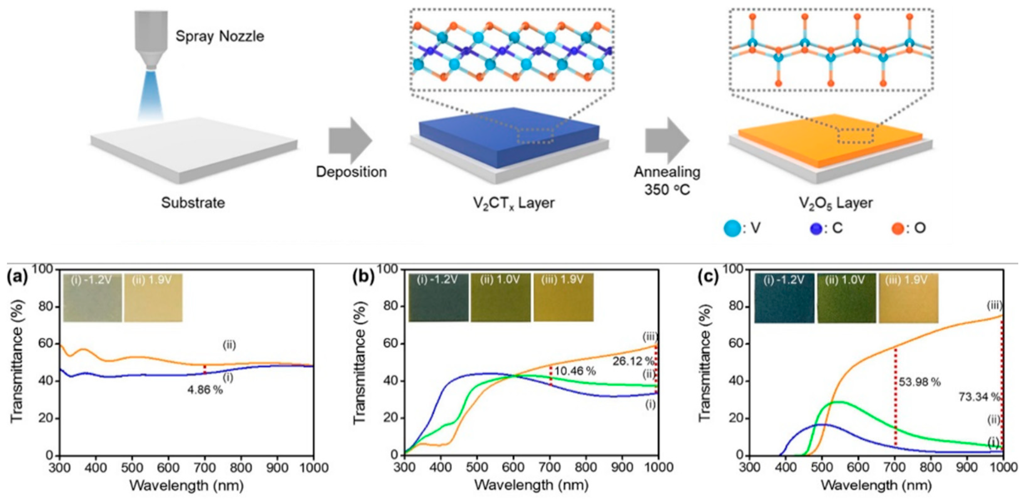
- Nguyen, V.-T.; Min, B.K.; Kim, S.K.; Yi, Y.; Choi, C.-G. A Flexible and High-Performance Electrochromic Smart Window Produced by WO3/Ti3C2Tx MXene Hybrids. J. Mater. Chem. C 2021, 9, 3183–3192. [Google Scholar] [CrossRef]
- Pugliese, M.; Scarfiello, R.; Prontera, C.T.; Giannuzzi, R.; Bianco, G.V.; Bruno, G.; Carallo, S.; Mariano, F.; Maggiore, A.; Carbone, L.; et al. Visible Light–Near-Infrared Dual-Band Electrochromic Device. ACS Sustain. Chem. Eng. 2023, 11, 9601–9612. [Google Scholar] [CrossRef]
- Wruck, D.A.; Rubin, M. Structure and Electronic Properties of Electrochromic NiO Films. J. Electrochem. Soc. 1993, 140, 1097–1104. [Google Scholar] [CrossRef]
- Šurca, A.; Orel, B.; Pihlar, B.; Bukovec, P. Optical, Spectroelectrochemical and Structural Properties of Sol-Gel Derived Ni-Oxide Electrochromic Film. J. Electroanal. Chem. 1996, 408, 83–100. [Google Scholar] [CrossRef]
- Boschloo, G.; Hagfeldt, A. Spectroelectrochemistry of Nanostructured NiO. J. Phys. Chem. B 2001, 105, 3039–3044. [Google Scholar] [CrossRef]
- Xia, X.H.; Tu, J.P.; Zhang, J.; Wang, X.L.; Zhang, W.K.; Huang, H. Morphology Effect on the Electrochromic and Electrochemical Performances of NiO Thin Films. Electrochim. Acta 2008, 53, 5721–5724. [Google Scholar] [CrossRef]
- Lampert, C.M.; Omstead, T.R.; Yu, P.C. Chemical and Optical Properties of Electrochromic Nickel Oxide Films. Sol. Energy Mater. 1986, 14, 161–174. [Google Scholar] [CrossRef]
- Arakaki, J.; Reyes, R.; Horn, M.; Estrada, W. Electrochromism in NiOx and WOx Obtained by Spray Pyrolysis. Sol. Energy Mater. Sol. Cells 1995, 37, 33–41. [Google Scholar] [CrossRef]
- Kadam, L.D.; Patil, P.S. Studies on Electrochromic Properties of Nickel Oxide Thin films Prepared by Spray Pyrolysis Technique. Sol. Energy Mater. 2001, 69, 361–369. [Google Scholar] [CrossRef]
- Mahmoud, S.A.; Akl, A.A.; Kamal, H.; Abdel-Hady, K. Opto-Structural, Electrical and Electrochromic Properties of Crystalline Nickel Oxide Thin Films Prepared by Spray Pyrolysis. Phys. B Condens. Matter 2002, 311, 366–375. [Google Scholar] [CrossRef]
- Wang, S.-Y.; Wang, W.; Wang, W.-Z.; Du, Y.-W. Preparation and Characterization of Highly Oriented NiO(200) Films by a Pulse Ultrasonic Spray Pyrolysis Method. Mater. Sci. Eng. B 2002, 90, 133–137. [Google Scholar] [CrossRef]
- Kamal, H.; Elmaghraby, E.K.; Ali, S.A.; Abdel-Hady, K. The Electrochromic Behavior of Nickel Oxide Films Sprayed at Different Preparative Conditions. Thin Solid Films 2005, 483, 330–339. [Google Scholar] [CrossRef]
- Lin, S.-H.; Chen, F.-R.; Kai, J.-J. Electrochromic Properties of Nano-Structured Nickel Oxide Thin Film Prepared by Spray Pyrolysis Method. Appl. Surf. Sci. 2008, 254, 2017–2022. [Google Scholar] [CrossRef]
- Romero, R.; Martin, F.; Ramos-Barrado, J.R.; Leinen, D. Synthesis and Characterization of Nanostructured Nickel Oxide Thin Films Prepared with Chemical Spray Pyrolysis. Thin Solid Films 2010, 518, 4499–4502. [Google Scholar] [CrossRef]
- Ismail, R.A.; Ghafori, S.; Kadhim, G.A. Preparation and Characterization of Nanostructured Nickel Oxide Thin Films by Spray Pyrolysis. Appl. Nanosci. 2013, 3, 509–514. [Google Scholar] [CrossRef]
- Sharma, R.; Acharya, A.D.; Shrivastava, S.B.; Shripathi, T.; Ganesan, V. Preparation and Characterization of Transparent NiO Thin Films Deposited by Spray Pyrolysis Technique. Optik 2014, 125, 6751–6756. [Google Scholar] [CrossRef]
- Gowthami, V.; Meenakshi, M.; Perumal, P.; Sivakuma, R.; Sanjeeviraja, C. Preparation of Rod Shaped Nickel Oxide Thin Films by a Novel and Cost Effective Nebulizer Technique. Mater. Sci. Semicond. Process. 2014, 27, 1042–1049. [Google Scholar] [CrossRef]
- Barir, R.; Benhaoua, B.; Benhamida, S.; Rahal, A.; Sahraoui, T.; Gheriani, R. Effect of Precursor Concentration on Structural Optical and Electrical Properties of NiO Thin Films Prepared by Spray Pyrolysis. J. Nanomater. 2017, 2017, 5204639. [Google Scholar] [CrossRef]
- Gomaa, M.M.; Yazdi, G.R.; Schmidt, S.; Boshta, M.; Khranovskyy, V.; Eriksson, F.; Farag, B.S.; Osman, M.B.S.; Yakimova, R. Effect of Precursor Solutions on the Structural and Optical Properties of Sprayed NiO Thin Films. Mater. Sci. Semicond. Process. 2017, 64, 32–38. [Google Scholar] [CrossRef]
- Chtouki, T.; Soumahoro, L.; Kulyk, B.; Bougharraf, H.; Kabouchi, B.; Erguig, H.; Sahraoui, B. Comparison of Structural, Morphological, Linear and Nonlinear Optical Properties of NiO Thin Films Elaborated by Spin-Coating and Spray Pyrolysis. Optik 2017, 128, 8–13. [Google Scholar] [CrossRef]
- Ravi Dhas, C.; Santhoshi Monica, S.E.; Venkatesh, R.; Sivakumar, R.; Nathanael, A.J.; Vignesh, R.; Arivukarasan, D.; Gnana Malar, K.C.M.; Keerthana, S. Correlation of Annealing Temperature on Physico-Chemical Properties and Electrochromic Performance of Nebulizer Spray-Coated NiO Films. Inorg. Nano-Metal Chem. 2023, 53, 178–190. [Google Scholar] [CrossRef]
- Obaida, M.; Fathi, A.M.; Moussa, I.; Afify, H.H. Characterization and Electrochromic Properties of NiO Thin Films Prepared Using a Green Aqueous Solution by Pulsed Spray Pyrolysis Technique. J. Mater. Res. 2022, 37, 2282–2292. [Google Scholar] [CrossRef]
- Chen, Z.; Dedova, T.; Acik, I.O.; Danilson, M.; Krunks, M. Nickel Oxide Films by Chemical Spray: Effect of Deposition Temperature and Solvent Type on Structural, Optical, and Surface Properties. Appl. Surf. Sci. 2021, 548, 149118. [Google Scholar] [CrossRef]
- Garduño, I.A.; Alonso, J.C.; Bizarro, M.; Ortega, R.; Rodríguez-Fernández, L.; Ortiz, A. Optical and Electrical Properties of Lithium Doped Nickel Oxide Films Deposited by Spray Pyrolysis onto Alumina Substrates. J. Cryst. Growth 2010, 312, 3276–3281. [Google Scholar] [CrossRef]
- Loyola Poul Raj, I.; Valanarasu, S.; Rimal Isaac, R.S.; Ramudu, M.; Bitla, Y.; Ganesh, V.; Yahia, I.S. The Role of Silver Doping in Tuning the Optical Absorption, Energy Gap, Photoluminescence Properties of NiO Thin Films for UV Photosensor Applications. Optik 2022, 254, 168634. [Google Scholar] [CrossRef]
- Sathisha, D.; Naik, K.G. Synthesis and Characterization of Cobalt Doped Nickel Oxide Thin Films by Spray Pyrolysis Method; AIP Conference Proceedings: Bikaner, India, 2018; p. 100021. [Google Scholar]
- Martinez-Luevanos, A.; Oliva, J.; Garcia, C.R.; Avalos-Belmontes, F.; Garcia-Lobato, M.A. Effect of Cobalt on the Electrochromic Properties of NiO Films Deposited by Spray Pyrolysis. Appl. Phys. A 2017, 123, 349. [Google Scholar] [CrossRef]
- Sharma, R.; Acharya, A.D.; Moghe, S.; Shrivastava, S.B.; Gangrade, M.; Shripathi, T.; Ganesan, V. Effect of Cobalt Doping on Microstructural and Optical Properties of Nickel Oxide Thin Films. Mater. Sci. Semicond. Process. 2014, 23, 42–49. [Google Scholar] [CrossRef]
- Moghe, S.; Acharya, A.D.; Panda, R.; Shrivastava, S.B.; Gangrade, M.; Shripathi, T.; Ganesan, V. Effect of Copper Doping on the Change in the Optical Absorption Behaviour in NiO Thin Films. Renew. Energy 2012, 46, 43–48. [Google Scholar] [CrossRef]
- Mani Menaka, S.; Umadevi, G.; Manickam, M. Effect of Copper Concentration on the Physical Properties of Copper Doped NiO Thin Films Deposited by Spray Pyrolysis. Mater. Chem. Phys. 2017, 191, 181–187. [Google Scholar] [CrossRef]
- Monica, S.E.S.; Dhas, C.R.; Venkatesh, R.; Sivakumar, R.; Vignesh, R.; Ferby, V.A. Nebulizer Sprayed Nickel-Manganese (Ni-Mn) Mixed Metal Oxide Nanocomposite Coatings for High-Performance Electrochromic Device Applications. J. Solid State Electrochem. 2022, 26, 1271–1290. [Google Scholar] [CrossRef]
- Brioual, B.; Ghannam, H.; Rossi, Z.; Aouni, A.; El-Habib, A.; Diani, M.; Addou, M.; Matassa, R.; Nottola, S.; Jbilou, M. Effect of In-Doping on Electrochromic Behavior of NiO Thin Films. Materialia 2023, 30, 101832. [Google Scholar] [CrossRef]
- Mrabet, C.; Ben Amor, M.; Boukhachem, A.; Amlouk, M.; Manoubi, T. Physical Properties of La-Doped NiO Sprayed Thin Films for Optoelectronic and Sensor Applications. Ceram. Int. 2016, 42, 5963–5978. [Google Scholar] [CrossRef]
- Tenent, R.C.; Gillaspie, D.T.; Miedaner, A.; Parilla, P.A.; Curtis, C.J.; Dillon, A.C. Fast-Switching Electrochromic Li+-Doped NiO Films by Ultrasonic Spray Deposition. J. Electrochem. Soc. 2010, 157, H318. [Google Scholar] [CrossRef]
- Kumar, A.; Sahay, P.P. Lithium Doping in Spray-Pyrolyzed NiO Thin Films: Results on Their Microstructural, Optical and Electrochromic Properties. Appl. Phys. A 2021, 127, 286. [Google Scholar] [CrossRef]
- Denayer, J.; Bister, G.; Simonis, P.; Colson, P.; Maho, A.; Aubry, P.; Vertruyen, B.; Henrist, C.; Lardot, V.; Cambier, F.; et al. Surfactant-Assisted Ultrasonic Spray Pyrolysis of Nickel Oxide and Lithium-Doped Nickel Oxide Thin Films, toward Electrochromic Applications. Appl. Surf. Sci. 2014, 321, 61–69. [Google Scholar] [CrossRef]
- Manceriu, L.M.; Colson, P.; Maho, A.; Eppe, G.; Nguyen, N.D.; Labrugere, C.; Rougier, A.; Cloots, R.; Henrist, C. Straightforward Prediction of the Ni1−xO Layers Stoichiometry by Using Optical and Electrochemical Measurements. J. Phys. D Appl. Phys. 2017, 50, 225501. [Google Scholar] [CrossRef]
- Carrillo-Delgado, C.; Arano-Martínez, J.A.; Vidales-Hurtado, M.A.; Torres-Torres, D.; Martínez-González, C.L.; Torres-Torres, C. Electrically Induced Directional Self-Focusing in Electrochromic NiO Thin Solid Films. J. Mater. Sci. Mater. Electron. 2023, 34, 953. [Google Scholar] [CrossRef]
- Garcia-Lobato, M.A.; Garcia, C.R.; Mtz-Enriquez, A.I.; Lopez-Badillo, C.M.; Garcias-Morales, C.; Muzquiz-Ramos, E.M.; Cruz-Ortiz, B.R. Enhanced Electrochromic Performance of NiO-MWCNTs Thin Films Deposited by Electrostatic Spray Deposition. Mater. Res. Bull. 2019, 114, 95–100. [Google Scholar] [CrossRef]
- Berlanga-Rodriguez, A.; Avalos-Belmontes, F.; Arvizu, M.A.; Garcia, C.R.; Rodríguez-Varela, F.J.; Oyervides-Muñoz, E.; Garcia-Lobato, M.A. Influence of the Diameter of Multi-Walled Carbon Nanotubes on the Electrochromic Performance of NiO Thin Films. Mater. Lett. 2021, 289, 129403. [Google Scholar] [CrossRef]
- Wang, J.; Zhu, R.; Gao, Y.; Jia, Y.; Cai, G. Unveiling the Multistep Electrochemical Desorption Mechanism of Cubic NiO Films for Transmissive-to-Black Electrochromic Energy Storage Devices. J. Phys. Chem. Lett. 2023, 14, 2284–2291. [Google Scholar] [CrossRef]
- Marrani, A.G.; Novelli, V.; Sheehan, S.; Dowling, D.P.; Dini, D. Probing the Redox States at the Surface of Electroactive Nanoporous NiO Thin Films. ACS Appl. Mater. Interfaces 2014, 6, 143–152. [Google Scholar] [CrossRef]
- Awais, M.; Dowling, D.P.; Decker, F.; Dini, D. Electrochemical Characterization of Nanoporous Nickel Oxide Thin Films Spray-Deposited onto Indium-Doped Tin Oxide for Solar Conversion Scopes. Adv. Condens. Matter Phys. 2015, 2015, 1–18. [Google Scholar] [CrossRef]
- Cogan, S.F.; Nguyen, N.M.; Perrotti, S.J.; Rauh, R.D. Optical Properties of Electrochromic Vanadium Pentoxide. J. Appl. Phys. 1989, 66, 1333–1337. [Google Scholar] [CrossRef]
- Šurca, A.; Orel, B.; Dražič, G.; Pihlar, B. Ex Situ and In Situ Infrared Spectroelectrochemical Investigations of V2O5 Crystalline Films. J. Electrochem. Soc. 1999, 146, 232–242. [Google Scholar] [CrossRef]
- Beke, S. A Review of the Growth of V2O5 Films from 1885 to 2010. Thin Solid Films 2011, 519, 1761–1771. [Google Scholar] [CrossRef]
- Mjejri, I.; Manceriu, L.M.; Gaudon, M.; Rougier, A.; Sediri, F. Nano-Vanadium Pentoxide Films for Electrochromic Displays. Solid State Ion. 2016, 292, 8–14. [Google Scholar] [CrossRef]
- Le, T.K.; Pham, P.V.; Dong, C.-L.; Bahlawane, N.; Vernardou, D.; Mjejri, I.; Rougier, A.; Kim, S.W. Recent Advances in Vanadium Pentoxide (V2O5) towards Related Applications in Chromogenics and beyond: Fundamentals, Progress, and Perspectives. J. Mater. Chem. C 2022, 10, 4019–4071. [Google Scholar] [CrossRef]
- Bouzidi, A.; Benramdane, N.; Nakrela, A.; Mathieu, C.; Khelifa, B.; Desfeux, R.; Da Costa, A. First Synthesis of Vanadium Oxide Thin Films by Spray Pyrolysis Technique. Mater. Sci. Eng. B 2002, 95, 141–147. [Google Scholar] [CrossRef]
- Boudaoud, L.; Benramdane, N.; Desfeux, R.; Khelifa, B.; Mathieu, C. Structural and Optical Properties of MoO3 and V2O5 Thin Films Prepared by Spray Pyrolysis. Catal. Today 2006, 113, 230–234. [Google Scholar] [CrossRef]
- Patil, C.E.; Tarwal, N.L.; Shinde, P.S.; Deshmukh, H.P.; Patil, P.S. Synthesis of Electrochromic Vanadium Oxide by Pulsed Spray Pyrolysis Technique and Its Properties. J. Phys. D Appl. Phys. 2009, 42, 025404. [Google Scholar] [CrossRef]
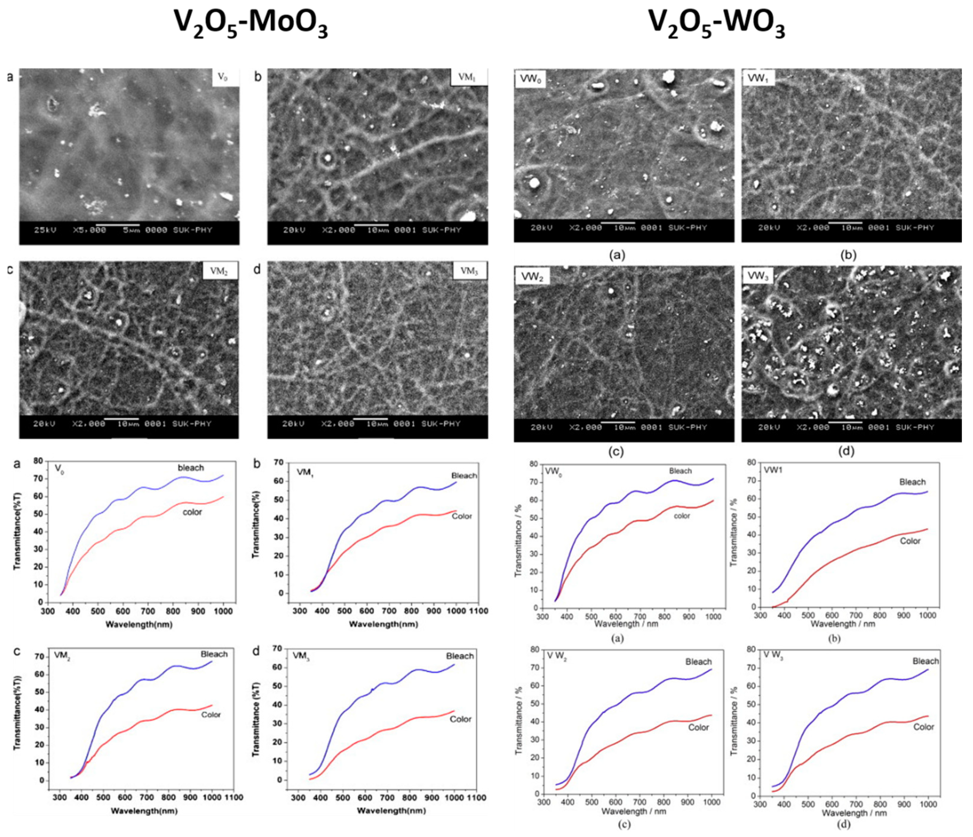
- Patil, C.E.; Jadhav, P.R.; Tarwal, N.L.; Deshmukh, H.P.; Karanjkar, M.M.; Patil, P.S. Electrochromic Performance of Mixed V2O5–MoO3 Thin Films Synthesized by Pulsed Spray Pyrolysis Technique. Mater. Chem. Phys. 2011, 126, 711–716. [Google Scholar] [CrossRef]
- Patil, C.E.; Jadhav, P.R.; Tarwal, N.L.; Deshmukh, H.P.; Karanjakar, M.M.; Wali, A.A.; Patil, P.S. Electrochromic Properties of Vanadium Oxide Thin Films Prepared by PSPT: Effect of Substrate Temperature. AIP Conf. Proc. 2013, 1536, 517–518. [Google Scholar] [CrossRef]
- Patil, C.E.; Tarwal, N.L.; Jadhav, P.R.; Shinde, P.S.; Deshmukh, H.P.; Karanjkar, M.M.; Moholkar, A.V.; Gang, M.G.; Kim, J.H.; Patil, P.S. Electrochromic Performance of the Mixed V2O5–WO3 Thin Films Synthesized by Pulsed Spray Pyrolysis Technique. Curr. Appl. Phys. 2014, 14, 389–395. [Google Scholar] [CrossRef]
- Hwang, K.S.; Kang, B.A.; Kim, S.D.; Hwangbo, S.; Kim, J.T. Amorphous Vanadium Pentoxide Thin Films Prepared by Electrostatic Spraying-Pyrolysis Deposition. Ceram. Int. 2012, 38, S645–S647. [Google Scholar] [CrossRef]
- Wei, Y.; Li, M.; Zheng, J.; Xu, C. Structural Characterization and Electrical and Optical Properties of V2O5 Films Prepared via Ultrasonic Spraying. Thin Solid Films 2013, 534, 446–451. [Google Scholar] [CrossRef]
- Abd–Alghafour, N.M.; Ahmed, N.M.; Hassan, Z.; Mohammad, S.M. Influence of Solution Deposition Rate on Properties of V2O5 Thin Films Deposited by Spray Pyrolysis Technique. AIP Conf. Proc. 2016, 1756, 090010. [Google Scholar]
- Margoni, M.M.; Mathuri, S.; Ramamurthi, K.; Babu, R.R.; Sethuraman, K. Sprayed Vanadium Pentoxide Thin Films: Influence of Substrate Temperature and Role of HNO3 on the Structural, Optical, Morphological and Electrical Properties. Appl. Surf. Sci. 2017, 418, 280–290. [Google Scholar] [CrossRef]
- Darroudi, N.; Eshghi, H. Effects of Nozzle-to-Substrate Distance and Annealing Atmospheres on V2O5 Thin Films Prepared by Spray Pyrolysis Technique. Mater. Sci. Eng. B 2020, 262, 114726. [Google Scholar] [CrossRef]
- Mouratis, K.; Tudose, V.; Romanitan, C.; Pachiu, C.; Tutunaru, O.; Suchea, M.; Couris, S.; Vernardou, D.; Emmanouel, K. Electrochromic Performance of V2O5 Thin Films Grown by Spray Pyrolysis. Materials 2020, 13, 3859. [Google Scholar] [CrossRef] [PubMed]
- Mouratis, K.; Tudose, I.V.; Bouranta, A.; Pachiu, C.; Romanitan, C.; Tutunaru, O.; Couris, S.; Koudoumas, E.; Suchea, M. Annealing Effect on the Properties of Electrochromic V2O5 Thin Films Grown by Spray Deposition Technique. Nanomaterials 2020, 10, 2397. [Google Scholar] [CrossRef] [PubMed]
- Zhang, S.; Chen, S.; Luo, Y.; Yan, B.; Gu, Y.; Yang, F.; Cao, Y. Large-Scale Preparation of Solution-Processable One-Dimensional V2O5 Nanobelts with Ultrahigh Aspect Ratio for Bifunctional Multicolor Electrochromic and Supercapacitor Applications. J. Alloys Compds 2020, 842, 155882. [Google Scholar] [CrossRef]
- Khmissi, H.; Mahmoud, S.A.; Akl, A.A. Investigation of Thermal Annealing Effect on the Microstructure, Morphology, Linear and Non-Linear Optical Properties of Spray Deposited Nanosized V2O5 Thin Films. Optik 2021, 227, 165979. [Google Scholar] [CrossRef]
- Tutel, Y.; Durukan, M.B.; Koc, S.; Koylan, S.; Cakmak, H.; Kocak, Y.; Hekmat, F.; Ozensoy, E.; Ozbay, E.; Udum, Y.A.; et al. Multichromic Vanadium Pentoxide Thin Films Through Ultrasonic Spray Deposition. J. Electrochem. Soc. 2021, 168, 106511. [Google Scholar] [CrossRef]
- Romanitan, C.; Tudose, I.V.; Mouratis, K.; Popescu, M.C.; Pachiu, C.; Couris, S.; Koudoumas, E.; Suchea, M. Structural Investigations in Electrochromic Vanadium Pentoxide Thin Films. Phys. Status Solidi 2022, 219, 2100431. [Google Scholar] [CrossRef]
- Mousavi, M.; Kompany, A.; Shahtahmasebi, N.; Bagheri-Mohagheghi, M.-M. Effect of S-Doping on Structural, Optical and Electrochemical Properties of Vanadium Oxide Thin Films Prepared by Spray Pyrolysis. Phys. Scr. 2013, 88, 065701. [Google Scholar] [CrossRef]
- Abyazisani, M.; Bagheri-Mohagheghi, M.M.; Benam, M.R. Study of Structural and Optical Properties of Nanostructured V2O5 Thin Films Doped with Fluorine. Mater. Sci. Semicond. Process. 2015, 31, 693–699. [Google Scholar] [CrossRef]
- Kovendhan, M.; Paul Joseph, D.; Manimuthu, P.; Sendilkumar, A.; Karthick, S.N.; Sambasivam, S.; Vijayarangamuthu, K.; Kim, H.J.; Choi, B.C.; Asokan, K.; et al. Prototype Electrochromic Device and Dye Sensitized Solar Cell Using Spray Deposited Undoped and ‘Li’ Doped V2O5 Thin Film Electrodes. Curr. Appl. Phys. 2015, 15, 622–631. [Google Scholar] [CrossRef]
- Tabatabai Yazdi, S.; Pilevar Shahri, R.; Shafei, S. First Synthesis of In-Doped Vanadium Pentoxide Thin Films and Their Structural, Optical and Electrical Characterization. Mater. Sci. Eng. B 2021, 263, 114755. [Google Scholar] [CrossRef]
- Mrigal, A.; Temsamani, R.; Addou, M.; Hssein, M.; El Jouad, M. Electrochromic Properties of Mo-Doped V2O5 Thin Films Deposited by Spray Pyrolysis Process. Eur. Phys. J. Appl. Phys. 2019, 86, 20301. [Google Scholar] [CrossRef]
- Gandasiri, R.; Sreelatha, C.J.; Nagaraju, P.; Vijayakumar, Y. Effect of Annealing Temperature on Micro-Structural, Optical and Electrical Characterization of Nanostructured V2O5 Thin Films Prepared by Spray Pyrolysis Technique. Phys. B Condens. Matter 2019, 572, 220–224. [Google Scholar] [CrossRef]
- Hsiao, Y.-S.; Chang-Jian, C.-W.; Syu, W.-L.; Yen, S.-C.; Huang, J.-H.; Weng, H.-C.; Lu, C.-Z.; Hsu, S.-C. Enhanced Electrochromic Performance of Carbon-Coated V2O5 Derived from a Metal–Organic Framework. Appl. Surf. Sci. 2021, 542, 148498. [Google Scholar] [CrossRef]
- Li, H.; Liang, H.; Li, R.; Lu, Z.; Hou, C.; Zhang, Q.; Li, Y.; Li, K.; Wang, H. Ultrafast, Stable Electrochromics Enabled by Hierarchical Assembly of V2O5@C Microrod Network. ACS Appl. Mater. Interfaces 2022, 14, 48037–48044. [Google Scholar] [CrossRef]
- Kim, J.; Lee, K.H.; Lee, S.; Park, S.; Chen, H.; Kim, S.K.; Yim, S.; Song, W.; Lee, S.S.; Yoon, D.H.; et al. Minimized Optical Scattering of MXene-Derived 2D V2O5 Nanosheet-Based Electrochromic Device with High Multicolor Contrast and Accuracy. Chem. Eng. J. 2023, 453, 139973. [Google Scholar] [CrossRef]
- Patil, P.S.; Patil, R.S. Studies on Spray Pyrolyzed Molybdenum Trioxide Thin Films. Bull. Mater. Sci. 1995, 18, 911–916. [Google Scholar] [CrossRef]
- Mahajan, S.S.; Mujawar, S.H.; Shinde, P.S.; Inamdar, A.I.; Patil, P.S. Structural, Morphological, Optical and Electrochromic Properties of Ti-Doped MoO3 Thin Films. Sol. Energy Mater. Sol. Cells 2009, 93, 183–187. [Google Scholar] [CrossRef]
- Kumar, A.; Prajapati, C.S.; Sahay, P.P. Results on the Microstructural, Optical and Electrochromic Properties of Spray-Deposited MoO3 Thin Films by the Influence of W Doping. Mater. Sci. Semicond. Process. 2019, 104, 104668. [Google Scholar] [CrossRef]
- Turel, O.; Hacioglu, S.O.; Coskun, S.; Toppare, L.; Unalan, H.E. Sequential Deposition of Electrochromic MoO3 Thin Films with High Coloration Efficiency and Stability. J. Electrochem. Soc. 2017, 164, E565. [Google Scholar] [CrossRef]
- Shinde, P.S.; Deshmukh, H.P.; Mujawar, S.H.; Inamdar, A.I.; Patil, P.S. Spray Deposited Titanium Oxide Thin Films as Passive Counter Electrodes. Electrochim. Acta 2007, 52, 3114–3120. [Google Scholar] [CrossRef]
- Dhandayuthapani, T.; Sivakumar, R.; Ilangovan, R.; Gopalakrishnan, C.; Sanjeeviraja, C.; Sivanantharaja, A.; Hari Krishna, R. Efficient Electrochromic Performance of Anatase TiO2 Thin Films Prepared by Nebulized Spray Deposition Method. J. Solid State Electrochem. 2018, 22, 1825–1838. [Google Scholar] [CrossRef]
- Enayati-Taloobaghi, H.; Eshghi, H. Achievement of High Electrochromic Performance of TiO2 Thin Films Prepared via Spray Pyrolysis Method, Influence of Annealing Process. Mater. Res. Bull. 2023, 167, 112416. [Google Scholar] [CrossRef]
- Zelazowska, E.; Rysiakiewicz-Pasek, E. Thin TiO2 Films for an Electrochromic System. Opt. Mater. 2009, 31, 1802–1804. [Google Scholar] [CrossRef]
- Liu, R.; Ren, Y.; Cai, H.; Zhang, C.; Wang, J.; Zhao, G.; Zhang, S. Fabrication of Electrochromic TiO2:Nb Films by Ultrasonic Spray Pyrolysis. Opt. Mater. 2022, 127, 112315. [Google Scholar] [CrossRef]
- Dhandayuthapani, T.; Sivakumar, R.; Ilangovan, R.; Sanjeeviraja, C.; Jeyadheepan, K.; Gopalakrishnan, C.; Sivaprakash, P.; Arumugam, S. Brown Coloration and Electrochromic Properties of Nickel Doped TiO2 Thin Films Deposited by Nebulized Spray Pyrolysis Technique. Thin Solid Films 2020, 694, 137754. [Google Scholar] [CrossRef]
- Mujawar, S.H.; Inamdar, A.I.; Patil, S.B.; Patil, P.S. Electrochromic Properties of Spray-Deposited Niobium Oxide Thin Films. Solid State Ion. 2006, 177, 3333–3338. [Google Scholar] [CrossRef]
- Mujawar, S.H.; Inamdar, A.I.; Betty, C.A.; Ganesan, V.; Patil, P.S. Effect of Post Annealing Treatment on Electrochromic Properties of Spray Deposited Niobium Oxide Thin Films. Electrochim. Acta 2007, 52, 4899–4906. [Google Scholar] [CrossRef]
- Romero, R.; Dalchiele, E.A.; Martín, F.; Leinen, D.; Ramos-Barrado, J.R. Electrochromic Behaviour of Nb2O5 Thin Films with Different Morphologies Obtained by Spray Pyrolysis. Sol. Energy Mater. Sol. Cells 2009, 93, 222–229. [Google Scholar] [CrossRef]
- Fan, H.; Yan, W.; Ding, Y.; Bao, Z. Using Flame-Assisted Printing to Fabricate Large Nanostructured Oxide Thin Film for Electrochromic Applications. Nanosc. Res. Lett. 2020, 15, 218. [Google Scholar] [CrossRef]
- Patil, P.S.; Sadale, S.B.; Mujawar, S.H.; Shinde, P.S.; Chigare, P.S. Synthesis of Electrochromic Tin Oxide Thin Films with Faster Response by Spray Pyrolysis. Appl. Surf. Sci. 2007, 253, 8560–8567. [Google Scholar] [CrossRef]
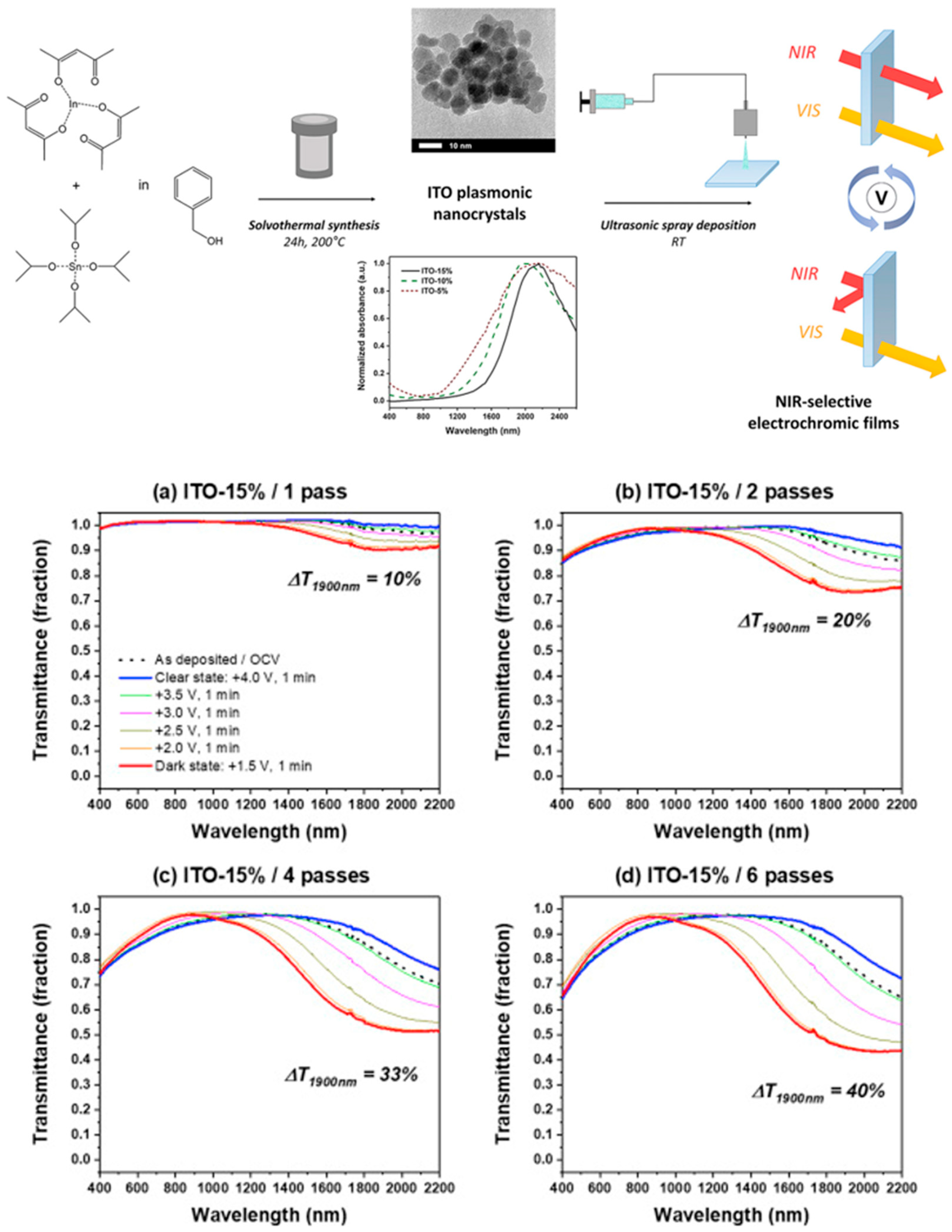
- Maho, A.; Comeron Lamela, L.; Henrist, C.; Henrard, L.; Tizei, L.H.G.; Kociak, M.; Stéphan, O.; Heo, S.; Milliron, D.J.; Vertruyen, B.; et al. Solvothermally-Synthesized Tin-Doped Indium Oxide Plasmonic Nanocrystals Spray-Deposited onto Glass as near-Infrared Electrochromic Films. Sol. Energy Mater. Sol. Cells 2019, 200, 110014. [Google Scholar] [CrossRef]
- Maho, A.; Saez Cabezas, C.A.; Meyertons, K.A.; Reimnitz, L.C.; Sahu, S.; Helms, B.A.; Milliron, D.J. Aqueous Processing and Spray Deposition of Polymer-Wrapped Tin-Doped Indium Oxide Nanocrystals as Electrochromic Thin Films. Chem. Mater. 2020, 32, 8401–8411. [Google Scholar] [CrossRef]
- Patil, P.S.; Kawar, R.K.; Sadale, S.B. Effect of Substrate Temperature on Electrochromic Properties of Spray-Deposited Ir-Oxide Thin Films. Appl. Surf. Sci. 2005, 249, 367–374. [Google Scholar] [CrossRef]
- Patil, P.S.; Mujawar, S.H.; Sadale, S.B.; Deshmukh, H.P.; Inamdar, A.I. Effect of Film Thickness on Electrochromic Activity of Spray Deposited Iridium Oxide Thin Films. Mater. Chem. Phys. 2006, 99, 309–313. [Google Scholar] [CrossRef]
- Hassanien, A.S.; Akl, A. Crystal Imperfections and Mott Parameters of Sprayed Nanostructure IrO2 Thin Films. Phys. B Condens. Matter 2015, 473, 11–19. [Google Scholar] [CrossRef]
- Vignesh, R.; Sivakumar, R.; Slimani, Y.; Sanjeeviraja, C. Molarity Influenced Interesting Electrochromic Optical Modulation Peak Shift in Nebulized Spray Deposited Mn3O4 Films. J. Electrochem. Soc. 2023, 170, 063506. [Google Scholar] [CrossRef]
- Patil, P.S.; Kadam, L.D.; Lokhande, C.D. Studies on Electrochromism of Spray Pyrolyzed Cobalt Oxide Thin Films. Sol. Energy Mater. Sol. Cells 1998, 53, 229–234. [Google Scholar] [CrossRef]
- Dhas, C.R.; Venkatesh, R.; Sivakumar, R.; Raj, A.M.E.; Sanjeeviraja, C. Fast Electrochromic Response of Porous-Structured Cobalt Oxide (Co3O4) Thin Films by Novel Nebulizer Spray Pyrolysis Technique. Ionics 2016, 22, 1911–1926. [Google Scholar] [CrossRef]
- Venkatesh, R.; Dhas, C.R.; Sivakumar, R.; Dhandayuthapani, T.; Sudhagar, P.; Sanjeeviraja, C.; Raj, A.M.E. Analysis of Optical Dispersion Parameters and Electrochromic Properties of Manganese-Doped Co3O4 Dendrite Structured Thin Films. J. Phys. Chem. Solids 2018, 122, 118–129. [Google Scholar] [CrossRef]
- Ravi Dhas, C.; Venkatesh, R.; Sivakumar, R.; Dhandayuthapani, T.; Subramanian, B.; Sanjeeviraja, C.; Moses Ezhil Raj, A. Electrochromic Performance of Chromium-Doped Co3O4 Nanocrystalline Thin Films Prepared by Nebulizer Spray Technique. J. Alloys Compd. 2019, 784, 49–59. [Google Scholar] [CrossRef]
- El Bachiri, A.; Soussi, L.; Karzazi, O.; Louardi, A.; Rmili, A.; Erguig, H.; El Idrissi, B. Electrochromic and Photoluminescence Properties of Cobalt Oxide Thin Films Prepared by Spray Pyrolysis. Spectrosc. Lett. 2019, 52, 66–73. [Google Scholar] [CrossRef]
- Özer, N. Optical Properties and Electrochromic Characterization of Sol–Gel Deposited Ceria Films. Sol. Energy Mater. Sol. Cells 2001, 68, 391–400. [Google Scholar] [CrossRef]
- Masetti, E.; Varsano, F.; Decker, F.; Krasilnikova, A. Sputter Deposited Cerium–Vanadium Oxide: Optical Characterization and Electrochromic Behavior. Electrochim. Acta 2001, 46, 2085–2090. [Google Scholar] [CrossRef]
- Avellaneda, C.O.; Bulhões, L.O.S.; Pawlicka, A. The CeO2–TiO2–ZrO2 Sol–Gel Film: A Counter-Electrode for Electrochromic Devices. Thin Solid Films 2005, 471, 100–104. [Google Scholar] [CrossRef]
- Verma, A.; Samanta, S.B.; Mehra, N.C.; Bakhshi, A.K.; Agnihotry, S.A. Sol–Gel Derived Nanocrystalline CeO2–TiO2 Coatings for Electrochromic Windows. Sol. Energy Mater. Sol. Cells 2005, 86, 85–103. [Google Scholar] [CrossRef]
- El Idrissi, B.; Addou, M.; Outzourhit, A.; Regragui, M.; Bougrine, A.; Kachouane, A. Sprayed CeO2 Thin Films for Electrochromic Applications. Sol. Energy Mater. Sol. Cells 2001, 69, 1–8. [Google Scholar] [CrossRef]
- Bhosale, A.K.; Tarwal, N.L.; Shinde, P.S.; Kadam, P.M.; Patil, R.S.; Barman, S.R.; Patil, P.S. Effective Utilization of Spray Pyrolyzed CeO2 as Optically Passive Counter Electrode for Enhancing Optical Modulation of WO3. Solid State Ion. 2009, 180, 1324–1331. [Google Scholar] [CrossRef]
- Dalavi, D.S.; Bhosale, A.K.; Desai, R.S.; Patil, P.S. Energy Efficient Electrochromic Smart Windows Based on Highly Stable CeO2-V2O5 Optically Passive Counter Electrode. Mater. Today Proc. 2021, 43, 2702–2706. [Google Scholar] [CrossRef]
- El-Habib, A.; Addou, M.; Aouni, A.; Zimou, J.; Diani, M.; Ftouhi, H.; Jouad, Z.E. Physical Properties and Electrochemical Behavior of Thin Layers of Vanadium Doped Cerium Dioxide. Surf. Interfaces 2021, 23, 100906. [Google Scholar] [CrossRef]
- Bhosale, A.K.; Shinde, P.S.; Tarwal, N.L.; Pawar, R.C.; Kadam, P.M.; Patil, P.S. Synthesis and Characterization of Highly Stable Optically Passive CeO2–ZrO2 Counter Electrode. Electrochim. Acta 2010, 55, 1900–1906. [Google Scholar] [CrossRef]
- Bhosale, A.K.; Kulal, S.R.; Gurame, V.M.; Patil, P.S. Spray Deposited CeO2–TiO2 Counter Electrode for Electrochromic Devices. Bull. Mater. Sci. 2015, 38, 483–491. [Google Scholar] [CrossRef]
- Thakur, V.K.; Ding, G.; Ma, J.; Lee, P.S.; Lu, X. Hybrid Materials and Polymer Electrolytes for Electrochromic Device Applications. Adv. Mater. 2012, 24, 4071–4096. [Google Scholar] [CrossRef]
- Yoo, S.J.; Lim, J.W.; Sung, Y.-E. Improved Electrochromic Devices with an Inorganic Solid Electrolyte Protective Layer. Sol. Energy Mater. Sol. Cells 2006, 90, 477–484. [Google Scholar] [CrossRef]
- Nguyen, C.A.; Argun, A.A.; Hammond, P.T.; Lu, X.; Lee, P.S. Layer-by-Layer Assembled Solid Polymer Electrolyte for Electrochromic Devices. Chem. Mater. 2011, 23, 2142–2149. [Google Scholar] [CrossRef]
- Cloots, R.; Henrist, C.; Denayer, J.; Maho, A.; Cambier, F.; Lardot, V.; Bister, G.; Aubry, P. Improved Process of Ultrasonic Spray Pyrolysis Deposition of One or More Electrochromic and/or Electrolytic Films on a Substrate. WO2016113050A1, 21 July 2016. [Google Scholar]
- Djenadic, R.; Botros, M.; Benel, C.; Clemens, O.; Indris, S.; Choudhary, A.; Bergfeldt, T.; Hahn, H. Nebulized Spray Pyrolysis of Al-Doped Li7La3Zr2O12 Solid Electrolyte for Battery Applications. Solid State Ion. 2014, 263, 49–56. [Google Scholar] [CrossRef]
- Fan, L.; Xie, H.; Su, P.-C. Spray Coating of Dense Proton-Conducting BaCe0.7Zr0.1Y0.2O3 Electrolyte for Low Temperature Solid Oxide Fuel Cells. Int. J. Hydrog. Energy 2016, 41, 6516–6525. [Google Scholar] [CrossRef]
- Liang, B.; Keshishian, V.; Liu, S.; Yi, E.; Jia, D.; Zhou, Y.; Kieffer, J.; Ye, B.; Laine, R.M. Processing Liquid-Feed Flame Spray Pyrolysis Synthesized Mg0.5Ce0.2Zr1.8(PO4)3 Nanopowders to Free Standing Thin Films and Pellets as Potential Electrolytes in All-Solid-State Mg Batteries. Electrochim. Acta 2018, 272, 144–153. [Google Scholar] [CrossRef]
- Mazel, A.; Rocco, L.; Penin, N.; Rougier, A. Oriented Surface-Anchored Metal–Organic Frameworks (SurMOFs) as Electrochromic Thin Films. Adv. Opt. Mater. 2023, 11, 2202939. [Google Scholar] [CrossRef]
- Liu, S.; Wei, C.; Wang, H.; Yang, W.; Zhang, J.; Wang, Z.; Zhao, W.; Lee, P.S.; Cai, G. Processable Nanoarchitectonics of Two-Dimensional Metallo-Supramolecular Polymer for Electrochromic Energy Storage Devices with High Coloration Efficiency and Stability. Nano Energy 2023, 110, 108337. [Google Scholar] [CrossRef]
- Gusatti, M.; Souza, D.A.R.; Ribeiro, S.J.L.; Nalin, M. An Electrolyte-Free Electrochromic Device Using Aluminum as Counter Electrode Material. Sol. Energy Mater. Sol. Cells 2023, 260, 112494. [Google Scholar] [CrossRef]
- Li, H.; Li, J.; Hou, C.; Ho, D.; Zhang, Q.; Li, Y.; Wang, H. Solution-Processed Porous Tungsten Molybdenum Oxide Electrodes for Energy Storage Smart Windows. Adv. Mater. Technol. 2017, 2, 1700047. [Google Scholar] [CrossRef]


| Reference | Spray Conditions (Tdep for Deposition Temperature, t.t. for Thermal Treatment) | Thickness (nm) | Tble (%) | Tcol (%) | ΔT (%) | tble (s) | tcol (s) | CE (cm2/C) | Cycling Runs |
|---|---|---|---|---|---|---|---|---|---|
| Colbow [72] | WCl6 in ethanol or DMF Tdep = 400 °C | N.p. | 75 | 2 | 73 | N.p. | N.p. | N.p. | N.p. |
| Colbow [73] | WCl6 in DMF Tdep = 200–400 °C | 250–650 | N.p. | N.p. | N.p. | N.p. | 40–120 | N.p. | N.p. |
| Colbow [74] | WCl6 in DMF Tdep = 200–400 °C | 450 | N.p. | N.p. | N.p. | N.p. | N.p. | N.p. | N.p. |
| Livage [75] | Tungstate/WOCl4 in H2O/alcohol Tdep = RT with drying at 80 °C | 500 | N.p. | N.p. | 0.7 (O.D.) | N.p. | N.p. | N.p. | N.p. |
| Estrada [76] | Ammonium tungstate in H2O Tdep = 430 °C | 1000 | 75 | 35 | 40 | N.p. | N.p. | N.p. | 100 |
| Regragui [77] | WCl6 in H2O–ethanol Tdep = 200–400 °C with t.t. at 500 °C | 150 | 60–72 | 10–50 | 22–60 | N.p. | N.p. | N.p. | N.p. |
| Regragui [78] | WCl6 in H2O–ethanol Tdep = 300 °C with t.t. at 500 °C | 150 | >80 | <5 | 75 | <5 | <10 | N.p. | N.p. |
| Patil [79] | NH4 tungstate & molybdate in H2O Tdep = 300 °C with t.t. at 400 °C | 600 | N.p. | N.p. | 0.6–1.3 (O.D.) | 2–3 | 4–5 | 42–63 | N.p. |
| Patil [80] | WO3 powder and C10H14O5Ti in NH4OH and methanol; Tdep = 525 °C | N.p. | 45–85 | 25–70 | 20–25 | N.p. | N.p. | 7–13 | N.p. |
| Patil [81] | WO3 powder and TiCl4 in NH4OH/H2O Tdep = 450 °C | N.p. | 50–73 | 45–67 | 2–10 | 3–6 | 4–5 | 8–26 | N.p. |
| Patil [82] | WO3 and Nb2O5 powders in NH4OH/H2O Tdep = 450 °C | 520–530 | 73–85 | 55–67 | 6–30 | 1–3 | 3–5 | 17–26 | N.p. |
| Patil [83] | WO3 and Nb2O5 powders in NH4OH/H2O Tdep = 450 °C | 510–530 | 65–75 | 52–58 | 10–20 | 6–8 | 5–7 | 13–19 | 1000 |
| Patil [84] | Ammonium tungstate in NH4OH/H2O Tdep = 450 °C | 200 | 70 | 65 | 5 | 3–4 | 5–6 | 25 | 1200 |
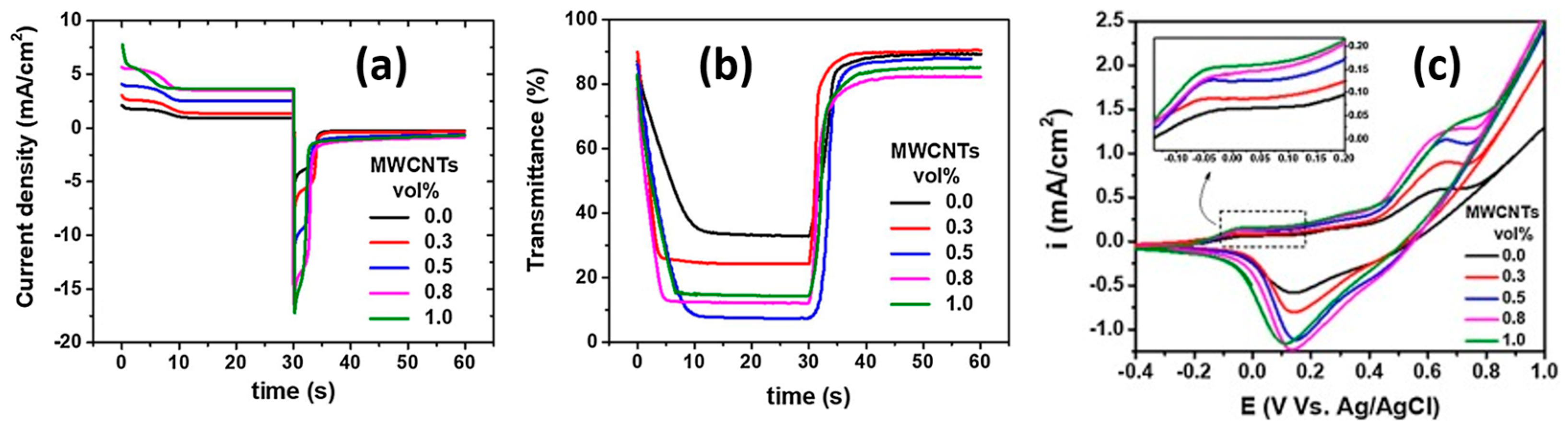
| Patil [85] | Ammonium tungstate and MWCNTs in H2O; Tdep = 450 °C | 250 | 75–80 | 30–50 | 30–45 | 3–6 | 6–8 | 43–79 | N.p. |
| Patil [86] | Ammonium tungstate in NH4OH/H2O Tdep = 450 °C | 250–750 | 25–80 | 10–63 | 10–50 | N.p. | N.p. | 14–43 | 1000 |
| Sivakumar [87] | Ammonium tungstate in NH4OH/H2O Tdep = 250 °C with t.t. at 500 °C | 600 | N.p. | N.p. | N.p. | N.p. | N.p. | N.p. | N.p. |
| Zelazowska [88] | WO(C5H7O2)4 in acetylacetone and dichloromethane; Tdep = 650 °C | 120 | 58 | 6 | 52 | N.p. | N.p. | N.p. | 100 |
| Sahay [89] | WCl6 or ammonium tungstate in DMF Tdep = up to 400 °C | 450–500 | N.p. | N.p. | N.p. | N.p. | N.p. | N.p. | N.p. |
| Acosta [90] | WCl6 and MoO2Cl2 in DMF Tdep = 500 °C | 480–520 | N.p. | N.p. | N.p. | N.p. | N.p. | N.p. | 2000 |
| Sahay [91] | Ammonium tungstate and MoCl5 in DMF Tdep = 390 °C | N.p. | 18–48 | 1–18 | 13–30 | 25–50 | 1–25 | 14–43 | 100 |
| Sahay [92] | Ammonium tungstate and SnCl4 in H2O Tdep = 400 °C | 500–550 | N.p. | N.p. | N.p. | N.p. | N.p. | N.p. | N.p. |
| Acosta [93] | WCl6 and TiCl3 in DMF Tdep = 500 °C | 480–520 | N.p. | N.p. | N.p. | N.p. | N.p. | N.p. | 3000 |
| Sahay [94] | Ammonium tungstate and SbCl3 in H2O Tdep = 400 °C | 450–470 | N.p. | N.p. | N.p. | 3–6 | 3–10 | N.p. | 50 |
| Mohagheghi [95] | WO3 powder, NiSO4, and CoCl2 in H2O Tdep = 400 °C with t.t. at 500 °C | 250 | N.p. | N.p. | N.p. | N.p. | N.p. | N.p. | N.p. |
| Mohagheghi [96] | WO3 powder + CoCl2 in H2O Tdep = 400 °C with t.t. at 500 °C | 250 | N.p. | N.p. | N.p. | N.p. | N.p. | N.p. | N.p. |
| Wolden [97] | WCl6 + ethanol + P123 Tdep = RT with t.t. at 300–400 °C | 400 | 70–92 | 14–38 | 35–75 | 6–120+ | 6–20 | 26–51 | 10 |
| Wolden [98] | WCl6 + ethanol + P123 Tdep = RT with t.t. at 300–400 °C | 400 | 70–80 | 45–50 | 40–75 | 5–24 | 5–9 | 43–50 | 2500 |
| Wolden [99] | WCl6 + ethanol + P123 Tdep = RT with t.t. at 350 °C | 1000 | 77–100 | 0–30 | 70–100 | 27–67 | 3 | 36–45 | 1000 |
| Duta [100] | WCl6 + ethanol Tdep = 200–300 °C | 200 | 65–80 | 15–35 | 21–64 | N.p. | N.p. | 28–35 | N.p. |
| Duta [101] | WCl6, HTAB, and PEG in ethanol and acetylacetone Tdep = 250 °C with t.t. at 410 °C | 350–375 | 65–80 | 45–50 | 13–35 | 47–58 | 13–19 | 10–43 | 50–100 |
| Cloots [102] | AMT and PEG in H2O Tdep = 350 °C | 550 | 92 | 9 | 83 | 42 | 72 | 28 | 500 |
| Cloots [103] | AMT and PEG in H2O Tdep = 350 °C | 100–120 | 87–92 | 7–9 | 78–85 | 46–51 | 77–91 | 26–31 | 100 |
| Cloots [104] | APTA and Brij-56 in H2O Tdep = 190 °C or 100 °C with t.t. at 350 °C | 200 | 55–85 | 20–55 | 10–40 | 35–200 | 60–300 | 6–40 | 20 |
| Lin [105] | WCl6 and P123 in ethanol Tdep = RT with t.t. at 350 °C | 1000 | 78–95 | 32–38 | 40–55 | 1–3 | 5–7 | N.p. | 3000 |
| Gesheva [106] | W powders and H2O2 in ethanol Tdep = RT with t.t. at 100–275 °C | 200 | N.p. | N.p. | 10–70 | N.p. | N.p. | 12–134 | N.p. |
| P.S. Lee [107] | H2WO4 and MoO3 in H2O and ethylene glycol; Tdep = RT with drying | 200 | 80 | 37 | 43 | 8 | 10 | 36 | 2000 |
| Elezzabi [108] | Ti–W–Mo oxides NPs in H2O Tdep = RT with drying at 60 °C | N.p. | 22–85 | 7–9 | 15–76 | N.p. | N.p. | N.p. | 100 |
| Elezzabi [109] | W-Mo NPs + PEDOT:PSS Tdep = 60 °C, layer-by-layer process | 900 | 75–85 | 10–30 | 55–65 | 11–14 | 18–22 | 22–53 | 300 |
| C.S. Lee [62] | WO3 NPs Tdep = 80 °C, NPDS | 400–700 | 60–70 | 5–20 | 44–64 | N.p. | N.p. | N.p. | N.p. |
| C.S. Lee [63] | WO3 NPs Tdep = RT-200 °C, NPDS | 400–700 | 55–65 | 14–35 | 10–42 | N.p. | N.p. | N.p. | N.p. |
| C.S. Lee [64] | WO3 NPs Tdep = 80 °C, NPDS | 400–700 | 2–15 | 55–62 | 43–55 | >40 | 18–30 | 42–77 | N.p. |
| C.S. Lee [110] | WO3 NPs Tdep = RT, NPDS | N.p. | 37–65 | 8–47 | 2–50 | Fixed time | Fixed time | N.p. | 600+ and over 1M |
| Tsukagoshi [111] | WO3 NPs in H2O Tdep = 150 to 300 °C | 450 | 79 | 19 | 60 | 2 | 4 | 37 | 80 |
| Liu [112] | WO3 and MoO3 NPs in H2O and ethanol Tdep not provided | N.p. | 70–75 | 12–36 | 45–60 | 6–11 | 4–9 | 43–80 | 2000 |
| Choi [113] | WO3 NPs + Ti3C2Tx MXene Tdep = RT with t.t. at 100 °C | 200 | 68–72 | 10–57 | 17–58 | 2–3 | 3–7 | 35–127 | 1000 |
| Pugliese [114] | WO3 and TiO2 NCs Tdep = 100 °C with t.t. at 300 °C | 500 | VIS: 71 NIR: 70 | VIS: 11 NIR: 5 | VIS: 60 NIR: 65 | VIS: 4 NIR: 22 | VIS: 22 NIR: 5 | VIS: 38 NIR: 29 | 500 |
| Reference | Spray Conditions (Tdep for Deposition Temperature, t.t. for Thermal Treatment) | Thickness (nm) | Tble (%) | Tcol (%) | ΔT (%) | tble (s) | tcol (s) | CE (cm2/C) | Cycling Runs |
|---|---|---|---|---|---|---|---|---|---|
| Arakaki [120] | Ni(NO3)2 in H2O Tdep = 220–400 °C | N.p. | 50+ | N.p. | 35 | N.p. | N.p. | 30 | 100+ |
| Patil [121] | NiCl2 in H2O Tdep = 350 °C | 300 | 80 | 60 | 20 | 40 | 20 | 37 | 500 |
| Mahmoud [122] | NiCl2 in H2O Tdep = 350 °C | 50–200 | N.p. | N.p. | 2–23 | N.p. | N.p. | N.p. | 150 |
| Wang [123] | Ni(NO3)2 in H2O Tdep = 200–400 °C | 4500 | N.p. | N.p. | N.p. | N.p. | N.p. | N.p. | N.p. |
| Abdel-Hady [124] | NiCl2 in H2O Tdep = 225–425 °C | 50–400 | 50–80 | 5–50 | 30–60 | 13 | 5 | 44 | 150 |
| Lin [125] | Ni(NO3)2 in ethanol Tdep = 200 °C with t.t. at 300 °C | 500 | 20–30 | 70–80 | 48–51 | 9–10 | 7–12 | N.p. | 3000 |
| Leinen [126] | Ni acetate in H2O Tdep = 350–450 °C | 230–840 | 20–70 (Tasdep) | N.p. | N.p. | N.p. | N.p. | N.p. | N.p. |
| Ismail [127] | NiCl2 in H2O Tdep = 280–400 °C | 200–900 | 65–70 (Tasdep) | N.p. | N.p. | N.p. | N.p. | N.p. | N.p. |
| Sharma [128] | NiCl2 in H2O Tdep = 350 °C | 70–110 | 60–90 (Tasdep) | N.p. | N.p. | N.p. | N.p. | N.p. | N.p. |
| Sanjeeviraja [129] | NiCl2 in H2O Tdep = 400 °C | 1100–2700 | 45–95 (Tasdep) | N.p. | N.p. | N.p. | N.p. | N.p. | N.p. |
| Benhaoua [130] | Ni(NO3)2 in H2O Tdep = 500 °C | 170–200 | 45–85 (Tasdep) | N.p. | N.p. | N.p. | N.p. | N.p. | N.p. |
| Gomaa [131] | NiCl2/Ni(NO3)2/Ni(OCOCH3)2 in H2O Tdep = 450 °C | 270–300 | 35–50 (Tasdep) | N.p. | N.p. | N.p. | N.p. | N.p. | N.p. |
| Chtouki [132] | NiCl2 in H2O Tdep = 350 °C with t.t. at 500 °C | 390 | 75 (Tasdep) | N.p. | N.p. | N.p. | N.p. | N.p. | N.p. |
| Ravi Dhas [133] | Ni(NO3)2 in H2O Tdep = 300 °C with t.t. at 400–550 °C | N.p. | N.p. | N.p. | 6–29 | 0.3–1.1 | 0.5–1.8 | 8–29 | 10 |
| Obaida [134] | Ni acetylacetonate in H2O Tdep = 400–500 °C | 190–400 | 20–60 (Tasdep) | N.p. | N.p. | N.p. | N.p. | N.p. | 500 |
| Krunks [135] | Ni acetate in H2O and isopropanol Tdep = 300–420 °C | 20–430 | 20–85 (Tasdep) | N.p. | N.p. | N.p. | N.p. | N.p. | N.p. |
| Ortiz [136] | Ni and Li acetates in H2O and methanol Tdep = 360–440 °C | 300–1000 | 10–50 (Tasdep) | N.p. | N.p. | N.p. | N.p. | N.p. | N.p. |
| Yahia [137] | NiCl2 + AgNO3 in H2O Tdep = 450 °C | 400–420 | N.p. | N.p. | N.p. | N.p. | N.p. | N.p. | N.p. |
| Naik [138] | Ni(NO3)2 + Co(NO3)2 in H2O Tdep = 400 °C | 700 | 5–20 (Tasdep) | N.p. | N.p. | N.p. | N.p. | N.p. | N.p. |
| Garcia-Lobato [139] | Ni and Co acetates in H2O and EtOH Tdep = 225 °C with t.t. at 300 °C | 310–380 | 50–60 | 4–6 | 46–54 | 13–18 | 18–25 | 27–32 | 65 |
| Ganesan [140] | NiCl2 and CoCl2 in H2O Tdep = 300 °C | 350 | 55–85 (Tasdep) | N.p. | N.p. | N.p. | N.p. | N.p. | N.p. |
| Ganesan [141] | NiCl2 and CuCl2 in H2O Tdep = 350 °C | N.p. | 35–50 (Tasdep) | N.p. | N.p. | N.p. | N.p. | N.p. | N.p. |
| Manickam [142] | NiCl2 and CuCl2 in H2O Tdep = 450 °C | N.p. | 20–45 (Tasdep) | N.p. | N.p. | N.p. | N.p. | N.p. | N.p. |
| Anslin Ferby [143] | Ni(NO3)2 and Mn(NO3)2 in H2O Tdep = 300 °C | N.p. | 60–75 | 30–45 | 29–37 | 0.2–1 | 0.4–1.1 | 29–105 | N.p. |
| Jbilou [144] | NiCl2 and InCl3 in H2O Tdep = 450 °C | 120 | 60–70 | 22–47 | 24–38 | N.p. | N.p. | 31–94 | N.p. |
| Mrabet [145] | NiCl2 and LaCl3 in H2O Tdep = 450 °C | N.p. | 30–55 (Tasdep) | N.p. | N.p. | N.p. | N.p. | N.p. | N.p. |
| Dillon [146] | Ni(NO3)2 and LiNO3 in H2O Tdep = 330 °C | N.p. | 83 | 33 | 50 | 57 | 29 | 33 | 50 |
| Sahay [147] | Ni(NO3)2 and Li acetate in H2O Tdep = 400 °C with t.t. at 500 °C | N.p. | 78–85 | 55–75 | 10–25 | N.p. | N.p. | 3–35 | N.p. |
| Cloots [148] | Ni(NO3)2 + LiNO3 + PEG in H2O Tdep = 350 °C | 300 | 89–97 | 45–58 | 39–43 | 8–17 | 29–115 | 31–41 | 100 |
| Cloots [149] | Ni(NO3)2 + PEG in H2O Tdep = 350 °C with t.t. at 350–600 °C | 200–300 | 70–80 | 65–70 | 5–10 | N.p. | N.p. | N.p. | 10 |
| Torres-Torres [150] | Ni acetate in PEG Tdep = 250 °C | 110 | 75 | 30 | 45 | N.p. | N.p. | N.p. | N.p. |
| Garcia-Lobato [151] | Ni(NO3)2 + MWCNTs in ethanol Tdep = 110 °C with t.t. at 350 °C | 110–200 | 80–90 | 10–30 | 40–80 | 2–7 | 4–10 | 26–31 | 5000 |
| Garcia-Lobato [152] | Ni(NO3)2 + MWCNTs in ethanol Tdep = 110 °C | 20–245 | 80–95 | 35–40 | 45–55 | N.p. | N.p. | 25–30 | 5000 |
| C.S. Lee [63] | NiO powder Tdep = RT-200 °C, NPDS | 400 | 75–80 (Tasdep) | N.p. | 55–65 (device) | N.p. | N.p. | N.p. | N.p. |
| Cai [153] | NiO NPs in ethanol Tdep not provided | 330–1600 | 90 | 10 | 83 | N.p. | N.p. | 76 | N.p. |
| Dini [154] | NiO NPs in alcohol Tdep = RT with t.t. at 450 °C | 200–4000 | N.p. | N.p. | N.p. | N.p. | N.p. | N.p. | N.p. |
| Dini [155] | NiO NPs in methanol Tdep = RT with t.t. at 450 °C | 200–3500 | N.p. | N.p. | N.p. | N.p. | N.p. | N.p. | 100 |
| Reference | Spray Conditions (Tdep for Deposition Temperature, t.t. for Thermal Treatment) | Thickness (nm) | Tble (%) | Tcol (%) | ΔT (%) | tble (s) | tcol (s) | CE (cm2/C) | Cycling Runs |
|---|---|---|---|---|---|---|---|---|---|
| Bouzidi [161] | VCl3 in H2O Tdep = 250 °C | N.p. | N.p. | N.p. | N.p. | N.p. | N.p. | N.p. | N.p. |
| Mathieu [162] | VCl3 in H2O Tdep = 150 °C | N.p. | 40 (Tasdep) | N.p. | N.p. | N.p. | N.p. | N.p. | N.p. |
| Patil [163] | VCl3 in methanol Tdep = 300 °C with t.t. at 400 °C | 120 | 49 | 32 | 17 | N.p. | N.p. | 13 | N.p. |
| Patil [164] | VCl3 and MoO3 in methanol Tdep = 400 °C + t.t. at 400 °C | 130–370 | 45–61 | 23–44 | 13–24 | 9–11 | 9–11 | 15–35 | N.p. |
| Patil [165] | VCl3 in methanol Tdep = 300–500 °C | N.p. | 36–61 | 23–44 | 8–17 | N.p. | N.p. | 10–15 | N.p. |
| Patil [166] | VCl3 and ammonium tungstate Tdep = 400 °C | 300–370 | 48–61 | 27–44 | 7–22 | 10–20 | 9–23 | 15–49 | 1000 |
| Kim [167] | V tri-isopropoxide in ethanol Tdep = 200 °C with t.t. at 200 °C | N.p. | 75 (Tasdep) | N.p. | N.p. | N.p. | N.p. | N.p. | N.p. |
| Wei [168] | V2O5 NPs in H2O Tdep = RT with drying at 110 °C | 30–120 | 70–85 (Tasdep) | N.p. | N.p. | N.p. | N.p. | N.p. | N.p. |
| Mohammad [169] | VCl3 in H2O Tdep = 350 °C | N.p. | 75–80 (Tasdep) | N.p. | N.p. | N.p. | N.p. | N.p. | N.p. |
| Ramamurthi [170] | NH4VO3 in H2O Tdep = 300–400 °C | N.p. | 62–78 (Tasdep) | N.p. | N.p. | N.p. | N.p. | N.p. | N.p. |
| Eshghi [171] | VCl3 in H2O Tdep not provided with t.t. at 200 °C | 600–2000 | 35–50 (Tasdep) | N.p. | N.p. | N.p. | N.p. | N.p. | N.p. |
| Mouratis [172] | NH4VO3 in H2O Tdep = 250 °C with t.t. at 400 °C | 1000 | 18–26 | 6–8 | 10–20 | 16–34 | 10–35 | N.p. | N.p. |
| Mouratis [173] | NH4VO3 in H2O Tdep = 250 °C with t.t. at 400 °C | N.p. | 40–43 | 31–32 | 8–12 | 15 | 10 | 4–6 | N.p. |
| Chen [174] | V2O5 powders Tdep = RT with drying at 70 °C | 690–800 | 80–36 | 33–39 | 4–42 | 4–9 | 1–7 | 8–83 | 1000 |
| Mahmoud [175] | V(NO3)5 in H2O Tdep = 350 °C with t.t. at 400–550 °C | 120–140 | 45–70 (Tasdep) | N.p. | N.p. | N.p. | N.p. | N.p. | N.p. |
| Unalan [176] | VO(acac)2 and V2O5 in methanol Tdep = 100 °C with t.t. at 450–550 °C | 60–80 | 75–94 | 64–94 | 0–18 | N.p. | N.p. | N.p. | 25 (1000 in devices) |
| Suchea [177] | NH4VO3 in H2O Tdep = 250 °C with t.t. at 400 °C | 100–800 | 12–65 | 1–60 | 5–11 | 2–34 | 2–35 | N.p. | N.p. |
| Mousavi [178] | VCl3 and (NH2)2CS in H2O Tdep = 400–450 °C | 110–270 | N.p. | N.p. | N.p. | N.p. | N.p. | N.p. | N.p. |
| Abyazisani [179] | VCl3 and NH4F in H2O Tdep = 450 °C | N.p. | N.p. | N.p. | N.p. | N.p. | N.p. | N.p. | N.p. |
| Kovendhan [180] | VCl3 and LiCl in H2O Tdep = 450 °C | 50–1400 | N.p. | N.p. | N.p. | N.p. | N.p. | N.p. | N.p. |
| Tabatabai [181] | VCl3 and InCl3 in H2O Tdep = 430 °C | N.p. | N.p. | N.p. | N.p. | N.p. | N.p. | N.p. | N.p. |
| Mrigal [182] | VCl3 and MoCl6 in H2O Tdep = 500 °C with t.t. at 400 °C | N.p. | 50–77 | 10–43 | 29–67 | N.p. | N.p. | 42–80 | N.p. |
| Sreelatha [183] | NH4VO3 and Triton-X 100 surfactant in H2O; Tdep = 300 °C with t.t. at 350–450 °C | 250 | 15–30 (Tasdep) | N.p. | N.p. | N.p. | N.p. | N.p. | N.p. |
| Hsiao [184] | VCl3 and PEDOT:PSS Tdep = RT with t.t. at 120 °C | N.p. | 68 | 14–42 | 20–46 | 3–7 | 4–8 | 39–89 | 10000 |
| Wang [185] | VCl3 and 1,4-benzendicarboxylic acid and HTAB in H2O/ethanol Tdep = 50 °C with t.t. at 50 °C | N.p. | 29–73 | 22–49 | 20–55 | 1–2 | 1–3 | 20–109 | 2000 |
| Kim [186] | V2CTx in H2O Tdep = 70 °C with t.t. at 350 °C | 600–1500 | 49–59 | 5–44 | 5–54 | 5–25 | 7–21 | 5–91 | 200 |
Disclaimer/Publisher’s Note: The statements, opinions and data contained in all publications are solely those of the individual author(s) and contributor(s) and not of MDPI and/or the editor(s). MDPI and/or the editor(s) disclaim responsibility for any injury to people or property resulting from any ideas, methods, instructions or products referred to in the content. |
© 2023 by the authors. Licensee MDPI, Basel, Switzerland. This article is an open access article distributed under the terms and conditions of the Creative Commons Attribution (CC BY) license (https://creativecommons.org/licenses/by/4.0/).
Share and Cite
Maho, A.; Nayak, S.; Gillissen, F.; Cloots, R.; Rougier, A. Film Deposition of Electrochromic Metal Oxides through Spray Coating: A Descriptive Review. Coatings 2023, 13, 1879. https://doi.org/10.3390/coatings13111879
Maho A, Nayak S, Gillissen F, Cloots R, Rougier A. Film Deposition of Electrochromic Metal Oxides through Spray Coating: A Descriptive Review. Coatings. 2023; 13(11):1879. https://doi.org/10.3390/coatings13111879
Chicago/Turabian StyleMaho, Anthony, Suraj Nayak, Florian Gillissen, Rudi Cloots, and Aline Rougier. 2023. "Film Deposition of Electrochromic Metal Oxides through Spray Coating: A Descriptive Review" Coatings 13, no. 11: 1879. https://doi.org/10.3390/coatings13111879