Article

Epitaxial Growth of Cobalt Oxide Thin Films on Sapphire Substrates Using Atmospheric Pressure Mist Chemical Vapor Deposition

Department of Materials Science and Engineering, I-Shou University, Kaohsiung City 84001, Taiwan
*
Authors to whom correspondence should be addressed.
Coatings 2023, 13(11), 1878; https://doi.org/10.3390/coatings13111878
Submission received: 3 September 2023 / Revised: 25 October 2023 / Accepted: 30 October 2023 / Published: 1 November 2023

Abstract

:
This study demonstrated the epitaxial growth of single-phase (111) CoO and (111) Co3O4 thin films on a-plane sapphire substrates using an atmospheric pressure mist chemical vapor deposition (mist-CVD) process. The phase structure of the grown cobalt oxide films was manipulated by controlling the growth temperature and process ambient, confirmed through X-ray diffraction, Raman spectroscopy, and X-ray photoelectron spectroscopy. Furthermore, the electrical properties of Co3O4 films were significantly improved after thermal annealing in oxygen ambient, exhibiting a stable p-type conductivity with an electrical resistivity of 8.35 Ohm cm and a carrier concentration of 4.19 × 1016 cm−3. While annealing CoO in oxygen atmosphere, the Co3O4 films were found to be most readily formed on the CoO surface due to the oxidation reaction. The orientation of the atomic arrangement of formed Co3O4 was epitaxially constrained by the underlying CoO epitaxial layer. The oxidation of CoO to Co3O4 was largely driven by outward diffusion of cobalt cations, resulting in the formation of pores in the interior of formed Co3O4 films.

1. Introduction

Metal oxide semiconductors are regarded as promising, next-generation, functional materials due to their various functionalities, including transparency, electrical conductivity, ferroelectricity, ferromagnetism, and superconductivity [1,2,3,4]. Thus, they are in demand for a wide range of applications, including transparent electronics, gas sensors, energy storage, thin film transistors, photodetectors, solar cells, catalysis, memory devices, etc. Most metal oxide semiconductors exhibit n-type conductivity, such as Al-doped ZnO, Sn-doped In2O3, and Sn-doped Ga2O3. However, several metal oxide semiconductors demonstrate p-type conductivity, including cobalt oxide, nickel oxide, and copper oxide [5]. Among these materials, cobalt oxide, studied in this work, has attracted intensive attention in the view of its applications in various fields, including photovoltaics devices [6,7], catalysis [8], gas sensors [9], water splitting [10], resistive switching [11], rechargeable batteries [12], supercapacitors [13], photodetectors [14], and spintronic devices [15]. There are two stable cobalt oxide phases: CoO (rock-salt structure, a = 0.426 nm) and Co3O4 (normal spinel structure, a = 0.808 nm). Both phases are direct band gap p-type semiconductors. CoO has a cubic rock-salt structure with high-spin Co2+ cations occupying the octahedral sites. Co3O4, on the other hand, has a normal spinel structure, with the mixed Co2+ and Co3+ cations occupying the tetrahedral and octahedral sites, respectively.
To date, cobalt oxide thin films have been successfully prepared through various methods, such as radio frequency reactive sputtering [7], spray pyrolysis [16], sol–gel [17], pulsed laser deposition (PLD) [18], molecular beam epitaxy (MBE) [19], atomic layer deposition (ALD) [20], and metalorganic chemical vapor deposition (MOCVD) [21]. The cobalt oxide thin films of both CoO and Co3O4 can be synthesized selectively by various thin film deposition technologies by controlling the process temperature and the composition of the reactive atmosphere during thin film deposition [18,22]. Furthermore, the increasing interest in the cobalt oxide thin films has prompted the development of epitaxial growth technology for obtaining high-quality single-crystalline films. In contrast to the polycrystalline films comprising randomly oriented grains, epitaxial film having well-ordered structures is essential to developing high-performance cobalt-oxide-based spintronic or optoelectronic devices. Although the epitaxial growth of cobalt oxide thin film can be implemented through PLD [18], MBE [19], ALD [20], and MOCVD [21], the processes mentioned above still need to adopt a high vacuum pumping system, complex gas transport system, or flammable and toxic organometallic precursors. In this study, we employed atmospheric pressure solution-processed mist chemical vapor deposition (mist-CVD) to perform the epitaxial growth of cobalt oxide films on sapphire substrates. Mist-CVD possesses the advantages of a non-vacuum system, low cost, low energy consumption, and non-toxicity. Furthermore, different works have shown that various functional metal oxide epitaxial films, including ZnO, Ga2O3, ZnGa2O4, In2O3, and SnO2, can be successfully grown using mist-CVD [23,24,25,26,27]. Therefore, the mist-CVD technique has great potential for application in the epitaxial growth of high-quality metal oxide thin films. However, to the best of our knowledge, less attention has been given to the study of the mist-CVD growth of cobalt oxide epitaxial films. Moreover, the selective epitaxial growth of single-phase CoO and Co3O4 films using mist-CVD by controlling growth conditions, such as temperature and ambient, has not been explored yet. This work demonstrated selective epitaxial growth of single-phase CoO and Co3O4 films on sapphire substrates via the atmospheric pressure mist-CVD process. In addition, the influence of post-annealing treatment on the electrical and structural properties of grown cobalt oxide films was also investigated in this work.

2. Materials and Methods

The epitaxial growth of cobalt oxide thin films was performed using an atmospheric pressure mist-CVD system. The details of the mist-CVD system can be found in our previous works [28]. Prior to the growth of cobalt oxide thin films, as received, a-plane sapphire substrates (12 mm × 12 mm) were cleaned ultrasonically in acetone for 10 min, rinsed with deionized water, and then blown with dry nitrogen. For the mist-CVD growth of cobalt oxide thin films, a precursor solution was prepared in a solution of 0.05 M cobalt (II) acetate tetrahydrate (Co(CH3COO)2 4H2O, 98%, Showa) dissolved into a solution of deionized water and acetic acid mixed in a 7:3 ratio. The precursor solution was atomized to produce mist droplets using ultrasonic transducers at 2.4 MHz and transferred into a reaction furnace, with a carrier gas of either nitrogen (N2, 99.99% purity) or oxygen (O2, 99.99%, purity), at a flow rate of 2 L/min. The growth of cobalt oxide films on sapphire substrates was implemented at the temperature of 450–500 °C for 60 min. The post-annealing treatment was implemented using an ULVAC MILA-5000 annealing system. The cobalt oxide films were annealed at 650 °C for 30 min under oxygen ambient.
The crystal structure of cobalt oxide films was analyzed using X-ray diffraction (XRD). A X’Pert PRO-MPD (PANalytical) diffractometer, equipped with a hybrid monochromator, was employed for conducting 2θ-ω scan measurements. Additionally, we used the D8 Discover (Bruker, Billerica, MA, USA) diffractometer for X-ray rocking curve (XRC) and φ-scan measurements. The Raman spectra were recorded using a Horiba Jobin Yvon HR800 system, using a 633 nm He-Ne laser as an excitation source. The surface morphologies of the grown films were examined through scanning electron microscopy (SEM, Hitachi, Tokyo, Japan, S3400). The chemical state of the cobalt oxide films was analyzed through X-ray photoelectron spectroscopy (XPS) using a JEOL JAMP 9500 F system. The electrical properties of the cobalt oxide films were examined through Hall-effect measurement (Ecopia, Anyang City, Republic of Korea, HMS-3000). The optical transmission spectrum was obtained using a UV-visible spectrophotometer (UV-Vis, Thermo Scientific, Waltham, MA, USA, Evolution 201). The microstructure of the cobalt oxide–sapphire interface was characterized using cross-sectional transmission electron microscopy (XTEM, JEOL JEM-2100F). The XTEM specimen was prepared using a focused ion beam (FIB, FEI, Nova-200 NanoLab). The high-resolution TEM (HRTEM) images were analyzed using Gatan Digital MicrographTM version 3.10.1 (Pleasanton, CA, USA) software.

3. Results

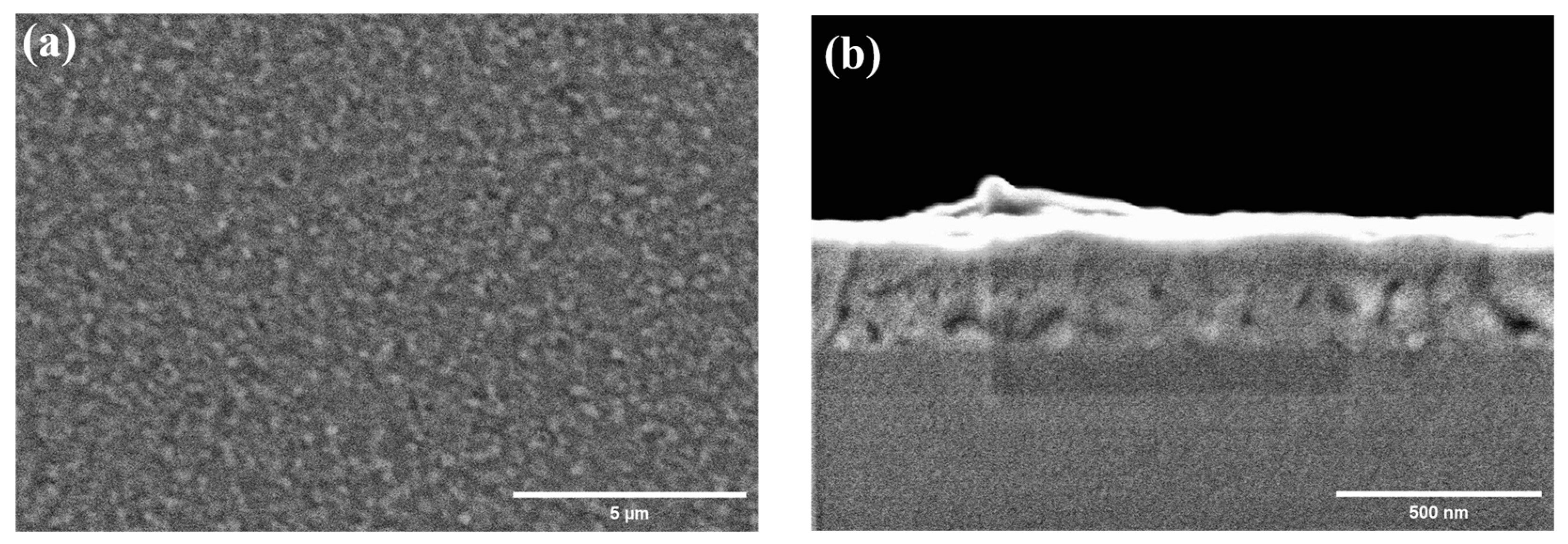
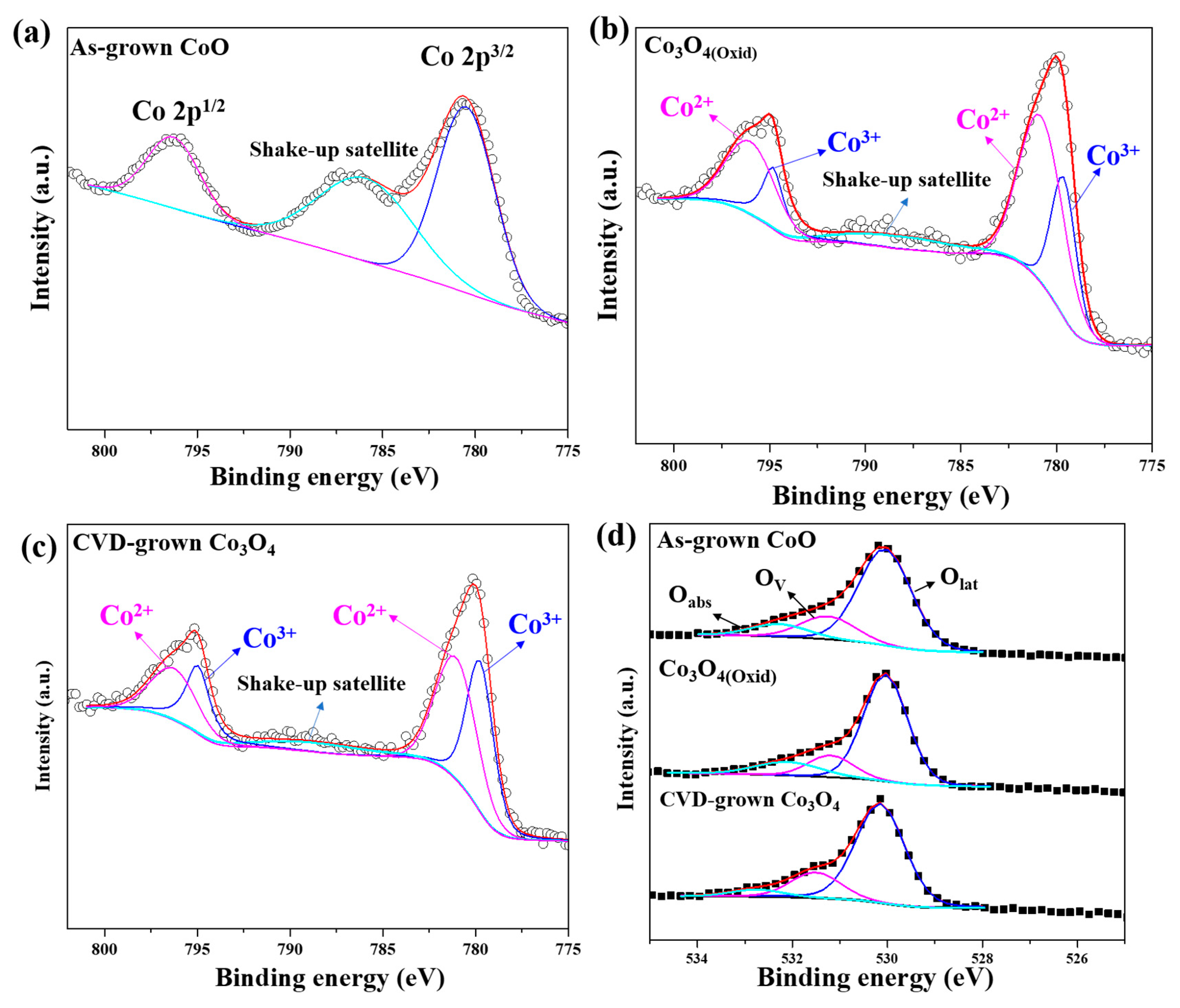
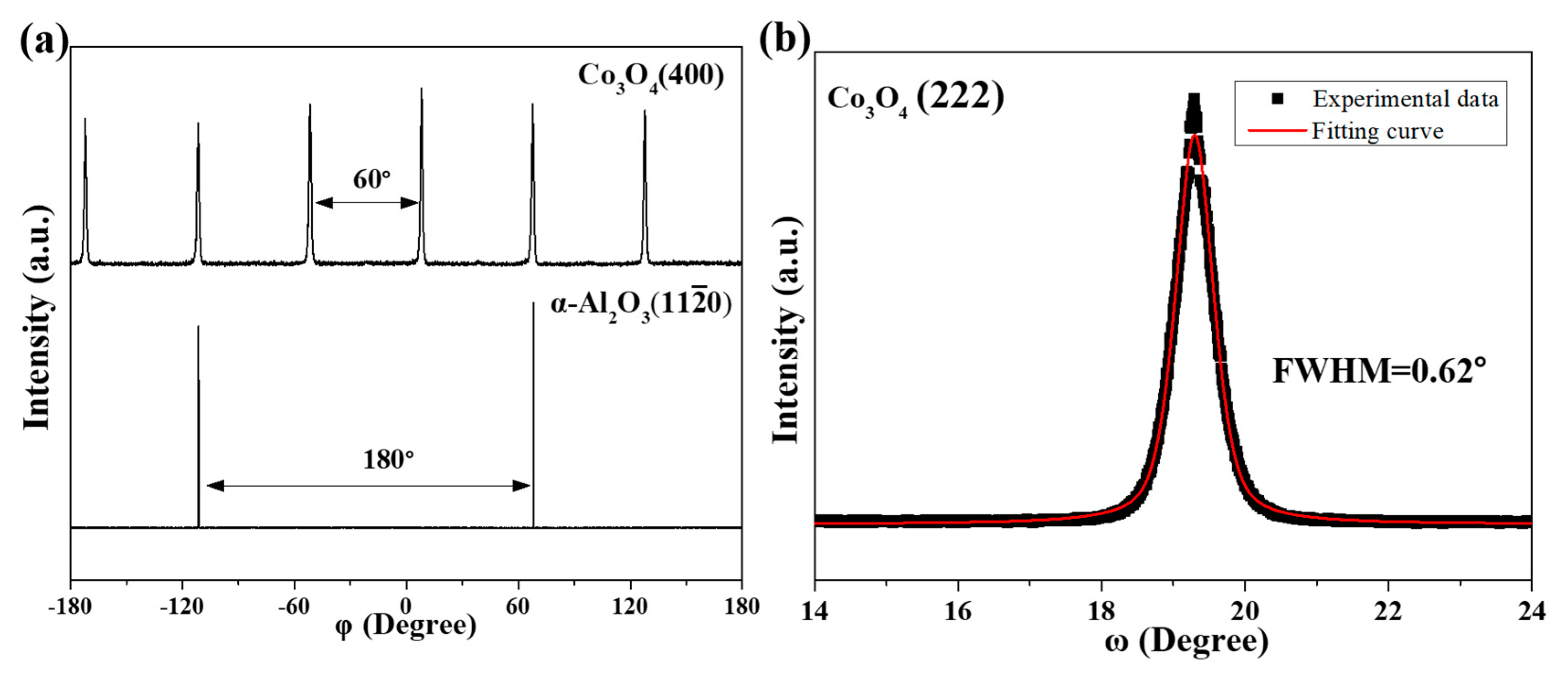
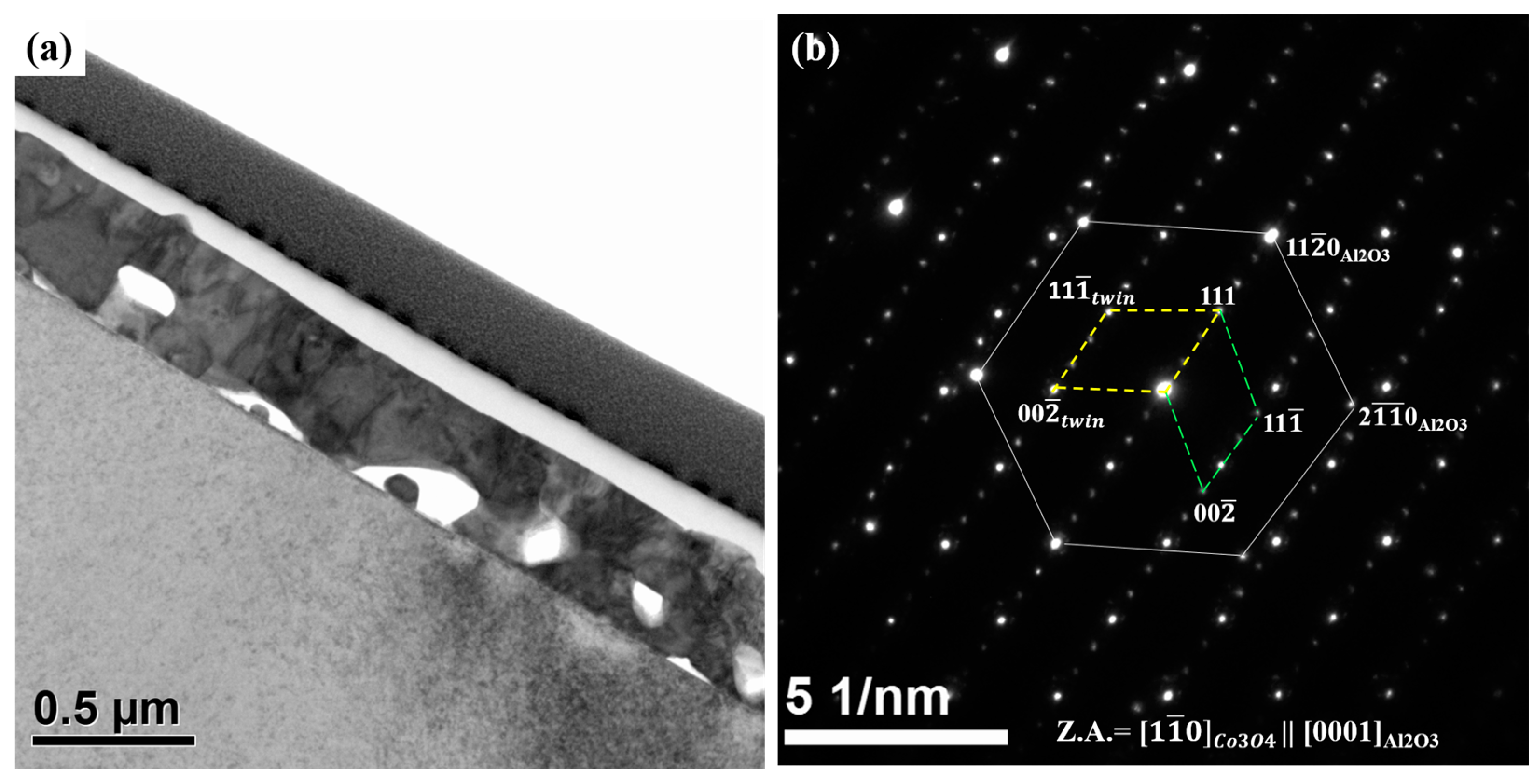
3.1. Epitaxial Growth of CoO and Co3O4 Thin Films on Sapphire Substrates

Based on previous successful work on the growth of ZnO epitaxial films using mist-CVD using the solution of zinc acetate dissolved into a solution of deionized water and acetate acid [28,29], we replaced zinc acetate with cobalt acetate in this work. The cobalt oxide thin films were grown at 450 and 500 °C using mist-CVD under nitrogen and oxygen ambient, respectively. We performed XRD to identify the phase of the grown films. Figure 1 depicts the 2θ-ω scan profiles of cobalt oxide thin films grown under various conditions. Figure 1b,c show the XRD profiles of the films grown under nitrogen ambient at 500 °C (Figure 1b) and oxygen ambient at the temperature of 450 °C (Figure 1c), respectively, revealing that the diffracted peaks at 2θ positions of 36.62° and 77.83° correspond to the (111) and (222) planes of the CoO phase (JCPDS No. 48-1719) and the diffracted peak at 38.59° and 59.42° corresponds to the (222) and (333) plane of the Co3O4 phase (JCPDS No. 42-1467), together with intense peaks of sapphire substrate (2θ = 37.7°). It is shown that CoO and Co3O4 phases coexisted in both grown cobalt oxide films. Notably, the cobalt oxide film grown under nitrogen ambient at the temperature of 450 °C solely exhibited a single CoO phase, as shown in Figure 1a. On the other hand, only the Co3O4 phase was detected in the cobalt oxide film grown at 500 °C under oxygen ambient, as shown in Figure 1d. Nevertheless, all of the cobalt oxide thin films grown on sapphire substrates under various conditions exhibited the <111> texture. The formation of CoO and Co3O4 significantly depends on the growth temperature and ambient. In general, the usage of metalorganic precursor containing only divalent Co2+ tends to favor the formation of a less stable CoO phase containing cobalt cations in a lower oxidation state (Co2+) [21,30]. However, they can still be used to grow the single-phase Co3O4 films comprising cobalt cations in two different oxidation states, Co2+ and Co3+, by adjusting CVD growth conditions (temperature and ambience). According to the abovementioned results, the use of divalent cobalt (cobalt (II) acetate) precursors for mist-CVD growth facilitated the growth of CoO films at relatively low temperatures in nitrogen (oxygen-deficient) atmosphere. On the other hand, the relatively high temperature and oxygen-rich atmosphere were beneficial for maintaining cobalt in its higher oxidation state, leading to the growth of single-phase Co3O4. The crystallite sizes of grown CoO and Co3O4 films can be estimated using the Scherrer method based on the results of the 2θ-ω scan [18,31]. Utilizing the Scherrer equation and the full-width at half-maximum (FWHM) of diffracted peaks corresponding to CoO (222) and Co3O4 (333), the average crystallite sizes of CoO and Co3O4 were determined to be 53 nm and 30 nm, respectively. In addition, the out-of-plane strains in both films were calculated from the 2θ positions of the diffracted peaks corresponding to CoO (222) and Co3O4 (333), and they were found to be −0.32% and −0.1%, respectively. These negative strains along the out-of-plane direction resulted from the presence of tensile in-plane strain in both of the grown epitaxial films. Furthermore, we carried out Raman analysis to explore the structural details in both of the cobalt oxide films grown at 450 °C in nitrogen ambient for CoO and 500 °C in oxygen ambient for Co3O4, respectively. Figure 2a,b display the corresponding Raman spectra of CoO and Co3O4 films. In Figure 2a, due to the NaCl-type centrosymmetric lattice structure, CoO exhibited a weak Raman scattering [32,33]. Except for the sharp peaks of sapphire substrates, as indicated by an asterisk, a broad asymmetric band with weak intensity appeared at 530 cm−1, indicated by a square mark. Although the first-order phonon scattering is forbidden based on the selection rules for the NaCl-type lattice structure, the presence of cobalt vacancy or other structural defects in the CoO lattice can lead to the emergence of the first-order phonon scattering. The broad band observed at 530 cm−1 can be attributed to this defect-induced one-phonon longitudinal optical (LO) Raman scatter [32]. The Raman spectrum of the Co3O4 film (Figure 2b) reveals the presence of five sharp peaks, which are located at 194, 482, 521, 619, and 691 cm−1. These peaks are in good agreement with the five Raman active phonon modes (A1g + 3F2g + Eg) associated with the spinel Co3O4 reported by Hadjiev et al. [34]. In comparison to CoO, the Co3O4 film exhibits lower optical transmittance at 633 nm, leading to the absorption of most incident lasers. However, CoO has higher optical transmittance and weaker Raman scattering due to its NaCl-type centrosymmetric lattice structure. This behavior is likely responsible for the appearance of Raman scattering corresponding to the underlying sapphire substrate. Based on the results of the XRD 2θ-ω scan and Raman scatter analysis, single-phase CoO and Co3O4 films can be obtained by controlling growth temperature and ambience during the mist-CVD process.
The corresponding surface morphologies of the CoO and Co3O4 films were observed through SEM, as shown in Figure 3a,b; both as-grown cobalt oxide films possessed uniform surface morphologies. The CoO film exhibited a flat and smooth surface morphology; however, the triangular-shaped grains could be observed on the surfaces of the Co3O4 films. The thicknesses of the CoO and Co3O4 films, which were grown for one hour, were approximately 294 nm and 180 nm, respectively, as shown in Figure 3c,d. In this work, the growth rates of single-phase CoO and Co3O4 epitaxial films were 294 nm and 180 nm/h, respectively, which were slower than those grown using other CVD processes (230–920 nm/h) [21,35]. The cross-sectional SEM image shown in Figure 3d reveals the presence of the columnar grain growth of Co3O4 on the sapphire substrate. The grain sizes measured from the cross-sectional SEM image ranged from 57 to 150 nm. Remarkably, the grain sizes observed through SEM are not equivalent to crystallite sizes estimated from XRD peak widths using the Scherrer equation because a grain may be composed of two or more crystallites.
Based on the results of XRD 2θ-ω scans, regardless of the growth conditions (growth temperature or ambient), the cobalt oxide films grown on a-plane sapphire substrates using mist-CVD exhibited <111> preferred orientation. To characterize the orientation relationship between cobalt oxide films and a-plane sapphire substrates, the XRD φ-scan measurement of CoO and Co3O4 films was performed, respectively. Figure 4a,b show the XRD φ-scan profiles of CoO and Co3O4 films grown on a-plane sapphire substrates. Remarkably, the XRD φ-scan profiles of {200} reflection of CoO film as well as {400} reflection of Co3O4 film exhibited six peaks separated by 60°, consisting of two sets of three-fold symmetric peaks separated by 60°, due to the crystal structures of rock salt CoO and spinel Co3O4 having three-fold symmetry along the <111> direction. This confirms the presence of 60°-rotated twin domains in either CoO or Co3O4 films grown on a-plane sapphire substrates. A single grain of CoO or Co3O4 can contain multiple twin domains, resulting in the small crystallite sizes determined using the Scherrer equation. Based on the results of XRD φ-scans, the obtained CoO films were epitaxially grown on sapphire substrate with the following epitaxial orientation relationship of (111)[1 1 ¯ 0]CoO||(11 2 ¯ 0)[0001]Al2O3; however, the epitaxial relationship between Co3O4 film and sapphire substrate was determined as (111)[11 2 ¯ ]Co3O4||(11 2 ¯ 0)[0001]Al2O3, indicating the rotation of the in-plane axis of Co3O4 film on sapphire substrate through an angle of 30° with respect to that of the CoO film. Moreover, the epitaxial qualities of cobalt oxide films were evaluated through the XRD rocking curve (XRC). Figure 4c,d show the XRC profiles of the CoO (111) plane and Co3O4 (222) plane, respectively. It was found that the FWHM values of both XRCs were 0.25°, determined by fitting a single pseudo-Voigt function, indicating that the epitaxial quality of the cobalt oxide films grown using atmospheric pressure mist-CVD was comparable to those grown using the conventional vacuum-based processes [18,20,35,36,37,38]. The threading dislocation densities of epitaxial films can be determined from the XRD rocking curves. The dislocation density (D) can be calculated using the measured FWHM of the XRC with the following equation [39]:
D = F W H M 2 / 2 π l n 2 · b 2
where b is the Burgers vector of dislocation. The Burgers vectors in both rock-salt and spinel structures are a 0 / 2 110 [40,41]; hence, the Burgers vectors of CoO and Co3O4 are 0.304 nm and 0.5716 nm, respectively. Thus, the dislocation densities in the CoO and Co3O4 epitaxial films were estimated to be 4.7 × 10 9 cm−2 and 1.3 × 10 9 cm−2, respectively.
The optical properties of CoO and Co3O4 epitaxial films were examined through UV-visible (UV-Vis) spectroscopy. Figure 5a,c are the UV-Vis transmission spectra of CoO and Co3O4 epitaxial films. The transmittance spectrum of the CoO film shows an absorption edge between approximately 400 and 500 nm. The average transmittance of CoO film in the visible region was in the range of 30–40%. For the Co3O4 epitaxial film, the corresponding UV-Vis spectrum (Figure 5c) shows an increase in the transmittance as the wavelength increases, with two absorptions at approximately 600 nm and 800 nm, respectively. The optical absorption coefficient (α) can be estimated from the transmittance (T) by the following equation:
α = l n T / d
where d is the film thickness. The optical bandgap (Eg) can be determined from (αhν)2 versus the hν plot (Tauc Plot), as shown in Figure 5b,d, where hν is the photon energy. The extrapolation of the linear region of the Tauc plot led to the optical bandgaps of the thin films. Based on Figure 5b, the optical bandgap of the CoO film was estimated to be 2.81 eV, consistent with that previously reported [18,22]. In contrast, the linearly fitted segments in the Tauc plot of the Co3O4 film (Figure 5d) prove the presence of two energy levels of the direct allowed transitions at 1.41 eV and 2.03 eV, respectively. As mixed Co2+ and Co3+ cations occupy the tetrahedral and octahedral sites in the spinel Co3O4 lattice, the charge transfer process associated with the Co3+–Co2+ and an oxide ligand (O2−) to metal (Co2+) transition, respectively, were identified. The bandgap of 1.41 eV corresponds to the Co3+–Co2+ charge transfer transition, reported within the range of 1.4–1.5 eV [16,21,22,42]. The bandgap of 2.03 eV is interpreted as an oxide ligand (O2−) to metal (Co2+) charge transfer transition, in agreement with the values (1.9–2.4 eV) reported in earlier studies [16,21,22,42].
The electrical properties of CoO films were evaluated using the Hall-effect measurement. The electrical resistivities of the as-grown CoO and Co3O4 films were 1.8 × 10⁵ Ω-cm and 2.3 × 10² Ω-cm, respectively, which are consistent with the values reported by other studies (>104 Ohm cm for CoO; 1~103 Ohm cm for Co3O4) [22]. Based on the results reported by previous studies, the electrical performance of various metal-oxide semiconductor films can be further improved via annealing at the temperature higher than that used in the film growth process [43,44]. Therefore, the annealing temperature of 650 °C, being higher than that used in the mist-CVD growth process, was chosen to further modify the electrical properties of the grown films. Notably, the electrical properties of CoO and Co3O4 films can be further improved using a post-thermal annealing treatment at 650 °C in oxygen ambient for 30 min. After thermal annealing, the electrical properties of annealed Co3O4 film were significantly enhanced, showing that the electrical resistivity was 8.35 Ohm cm, and the carrier concentration, with a positive Hall coefficient sign, increased from 1.5 × 1015 cm−3 to 4.19 × 1016 cm−3. In contrast, the as-grown CoO film behaved almost as an electrical insulator due to its extremely high electrical resistivity and low carrier concentration (2.3 × 1012 cm−3). When annealing the sample of CoO film in oxygen ambient, the sample showed p-type conductivity with the electrical resistivity and carrier concentration of 14.2 Ohm cm and 4.37 × 1016 cm−3. Annealing in an oxygen atmosphere significantly improves the electrical properties of both cobalt oxide thin films, which can increase carrier concentration to the order of magnitude of 1016 cm−3. When annealing in an oxygen-rich environment, the cobalt vacancies are the dominant point defects in cobalt oxide lattices and act as electron acceptors, which are the origin of hole carriers and p-type conductivity [45]. For the annealing of CoO film, the oxidation of CoO to Co3O4 readily occurred while heating at 300–650 °C in the presence of oxygen [46]. Therefore, the possible reason for improved electrical conductivity in the samples of annealed CoO film is attributed to the transformation into the Co3O4 phase through an oxidation process.

3.2. Thermal Annealing of CoO Epitaxial Films

Although improved electrical conductivity in the samples of annealed CoO film can possibly be attributed to the formation of the Co3O4 phase, the details of microstructural and chemical information of Co3O4 converted from CoO was unknown. Thus, the main aim of this study in this section is to explore the microstructural evolution during phase transition from CoO to Co3O4. To further prove the phase transition of CoO to Co3O4 during thermal annealing, XRD and Raman measurements were implemented, respectively, as shown in Figure 6. The result of the 2θ-ω scan profile revealed that the phase corresponding to the annealed sample of CoO film was Co3O4 (Figure 6a). The average crystallite size of the corresponding Co3O4 film was 35 nm, which was estimated from the diffraction peak width using the Scherrer equation. In addition, the Raman spectrum recorded from the annealed sample was consistent with the typical characteristic Raman peaks of spinel Co3O4 (Figure 6b). From the above results, it is shown that cobalt monoxide (CoO) was fully converted to tricobalt tetroxide (Co3O4) through an oxidation reaction, labeled as Co3O4(Oxid), during the annealing process in oxygen ambient. Figure 7 shows the top-view and cross-sectional SEM images of the annealed CoO film (Co3O4(Oxid)). In contrast to the flat surface of the CoO film before the annealing process (Figure 3a), the surface of the annealed CoO film exhibited an undulating and uneven morphology (Figure 7a). The average thickness of the annealed CoO film was approximately 300 nm. The density of CoO (6.45 g/cm3) is higher than that of Co3O4 (6.11 g/cm3). Thus, while CoO films were transformed into Co3O4 during thermal annealing, the volume (thickness) of the formed Co3O4 films was slightly increased. Remarkably, the pore-like structures present in the interiors of the films can be observed from the cross-sectional SEM image (Figure 7b). The details regarding the microstructure need to be further characterized through TEM and will be discussed in the following paragraphs.
To further investigate the valence and chemical state, X-ray photoelectron spectroscopy was used to characterize as-grown CoO, Co3O4 converted from CoO (Co3O4(Oxid)), and CVD-grown Co3O4 films. Figure 8 shows survey spectra of as-grown CoO, Co3O4 converted from CoO (Co3O4(Oxid)), and CVD-grown Co3O4 films. These XPS spectra dominantly show the element of Co and O along with the signal of carbon impurity (C 1s). The corresponding atomic concentrations (at.%) of cobalt were 48.3, 35.7, and 35.1 at.%, respectively, which were lower than those of cobalt oxides with stoichiometry (CoO: 50 at.%; Co3O4: 42.9 at.%). This confirms that all of the cobalt oxide films were metal-deficient-type oxides, indicating that cobalt vacancies were the dominant point defects in cobalt oxide lattices. The Co 2p spectra of CoO, Co3O4(Oxid), and CVD-grown Co3O4, are shown in Figure 8a–c. The Co 2p core level splits into 2p3/2 and 2p1/2 due to spin–orbit coupling. For as-grown CoO film (Figure 9a), the spin–orbit doublet was observed at a binding energy (B.E.) of 780 and 795.8 eV with a spin–orbit splitting of 15.8 eV between Co 2p3/2 and 2p1/2 core levels, along with an intense shake-up satellite peak at 786 eV, consistent with the characteristic XPS spectrum of CoO reported by other literatures [22,47]. The Co 2p spectrum of the Co3O4(Oxid) film (Figure 9b) was similar to that of the CVD-grown Co3O4 film (Figure 9c). The two main peaks corresponding to Co 2p3/2 and Co 2p1/2 core levels were located at 780 and 795.1 eV with spin–orbit splitting of 15.1 eV, together with a weak and broadened shake-up satellite peak located at 789 eV, consistent with the characteristic XPS spectrum of Co3O4 reported by other studies [10,22]. The Co2+ and Co3+ cations coexist in Co3O4; therefore, the Co 2p doublet peaks can be deconvoluted into four subpeaks, where the fitting peaks at 779.6 and 794.8 eV are assigned as the Co3+ state and the fitting peaks at 781 and 796 eV are ascribed to the Co2+ state. The signals of Co3+ and Co2+ in the Co 2p spectra were numerically integrated to obtain the ratios of Co3+/Co2+ cations of Co3O4(Oxid) and CVD-grown Co3O4 films, respectively, estimated to be 0.50 and 0.89, respectively, which are both lower than the theoretical ratio of Co3+/Co2+ in Co3O4 (2:1). The Co3+ vacancies (VCo3+) at the octahedral sites in spinel Co3O4 were indicated to dominate in both samples [45]. Remarkably, compared to CVD-grown Co3O4, Co3O4(Oxid) thin films, converted from CoO to Co3O4, revealed a lower Co3+/Co2+ratio, possibly due to the initial CoO phase solely comprising divalent cobalt. Theoretical and experimental studies have proven that the formation of the cation vacancies in metal oxides is favorable in an oxygen-rich environment [7,45,48]. Thus, the Co vacancies in Co3O4 were regarded as the major origin of their p-type semiconducting properties. The O 1s spectra of CoO, Co3O4(Oxid), and CVD-grown Co3O4, as shown in Figure 9d, are deconvoluted into three components at approximately 530, 531.2, and 532.2 eV, which is attributed to oxygen bonded with cobalt in the lattice (Olat), hydroxyl groups bonded to surface defects, such as oxygen vacancies (OV), and weakly absorbed molecular water (Oabs), respectively. The difference between the three O 1s core level XPS spectra recorded from CoO, Co3O4(Oxid), and CVD-grown Co3O4 films was not obvious. The contribution of oxygen bonded to cobalt in the lattice was estimated to be 72.8%, 72.0%, and 75.6%, respectively, indicating that all of the cobalt oxide films retain more structural oxygen in the lattice. Considering a water/acetate solution of cobalt acetate used as the cobalt source, the incorporation of carbon from the source is still possible [49]. Therefore, the residual impurities, such as carbon, in grown films were also detected through XPS. Although the signal of carbon 1s core level emission was not detected from the sample after argon ion sputtering, as shown in Figure S1 in Supplementary information, it is possible that the carbon content was below the instrument detection limit. In future work, secondary ion mass spectroscopy (SIMS) is needed for the detection of the residual impurity with low concentration.
According to the studies reported on the oxidation of CoO to Co3O4, the formation of the Co3O4(Oxid) layer initially occurs on the surface of CoO [50,51]. Therefore, the crystallographic alignment of the Co3O4(Oxid) film formed through the oxidation reaction is closely related to the orientation of the underlying CoO epitaxial film [50,51]. The X-ray diffraction φ-scan and XRC analysis were employed to assess the relationship and the crystalline quality of the formed Co3O4(Oxid) film. Figure 10a shows the XRD φ-scan profiles for the Co3O4(Oxid) film detecting Co3O4 (400) and Al2O3 (11 2 ¯ 0) reflections. The profile of the Co3O4(Oxid) film revealed six-fold symmetry with a spacing of 60°, indicating that the Co3O4(Oxid) film was in epitaxy with the sapphire substrate. Similarly, the presence of 60°-rotated twin domains in the Co3O4(Oxid) film was detected from the X-ray diffraction φ-scan profile. Interestingly, the crystallographic relationship between the Co3O4(Oxid) film and sapphire is (111)[1 1 ¯ 0]Co3O4(Oxid)||(11 2 ¯ 0)[0001]Al2O3, rotated through an angle of 30° with respect to that of CVD-grown Co3O4 film on sapphire substrate ((111)[11 2 ¯ ]Co3O4||(11 2 ¯ 0)[0001]Al2O3), as shown in Figure 4b. In Figure 10b, the Co3O4(Oxid) presents a broader FWHM (0.62°) of XRC for Co3O4 (222) diffraction. According to the cross-sectional SEM observation (Figure 7b), there were several pore-like structures in the interiors of the Co3O4(Oxid) films. These pore-like structures affected the growth of crystallites during the annealing process and were possibly responsible for the broader width of the XRC. The formation of the Co3O4 layer initially occurred on the surface of CoO. Sequentially, the entire CoO layer was gradually converted into Co3O4 during the oxidation process, as illustrated in Figure 11. The oxygen sublattices of the CoO and Co3O4, both being fcc sublattices, are nearly identical, with a lattice mismatch of about 5% [50]. Therefore, the oxygen sublattice of newly formed Co3O4(Oxid) inherited the original framework of CoO and was epitaxially constrained by the lattice planes of the underlying CoO, as illustrated in Figure 10.
We performed cross-sectional TEM to gain insight into the microstructure of the Co3O4(Oxid) film converted from CoO. Importantly, several pores present in the interior of Co3O4(Oxid) films were observed from the low-magnification bright-field TEM image (Figure 12a). During the oxidation of CoO to Co3O4, the growth of Co3O4 is initiated on the surface of CoO. Then, the Co3O4 layer grows inward and outward simultaneously [52,53,54]. In the case of outward growth, the formation of Co3O4 occurs due to the outward diffusion of cobalt cations and electrons as a result of the following reaction [52,53,54]:
3 C o i · · + 6 e + 2 O 2 C o 3 O 4
where C o i · · and e denote the double ionized interstitial cobalt cation and a free electron, respectively. The migrating interstitial cobalt cations reacted with oxygen on the surface to form Co3O4. In the case of inward growth, the reaction occurred at the interface between CoO and Co3O4, according to the displacement reaction [52,53,54]:
4 C o O C o 3 O 4 + C o i · · + 2 e
Based on the marker experiment for studying the oxidation of CoO, it was observed that cobalt cations continued to diffuse outward through the Co3O4 layer during the oxidation reaction [53,54]. Consequently, this resulted in the excessive concentration of cobalt vacancies inside the film layer due to the directional diffusion cobalt cations (the so-called Kirkendall effect). Thus, the thickness of formed Co3O4 films became thicker after the annealing process. The formation of pores was the consequence of a supersaturation of vacancies in the lattice brought about by the coalescence of cobalt vacancies [52,54]. In Figure 12b, the pattern of the selected area electron diffraction (SAED) recorded from the interface region shows the presence of two twinned variants in the formed Co3O4(Oxid) film, designated by green and yellow dashed lines, both indexed as the normal and 60°-rotated twin variants, respectively. They were oriented epitaxially with respect to the sapphire substrate. The epitaxial relationship between Co3O4(Oxid) and the sapphire substrate was identified as (111)[1 1 ¯ 0]Co3O4(Oxid)||(11 2 ¯ 0)[0001]Al2O3, which is consistent with the result of the XRD φ-scan, as shown in Figure 10a. Despite the presence of numerous pore structures in the formed Co3O4(Oxid) layer, the diffraction pattern of the Co3O4(Oxid) film remained consistent throughout the entire film layer.
The microstructure near the film/substrate heterointerface was visualized using HRTEM, as shown in Figure 13a. This view is along the sapphire [0001] zone axis. Remarkably, the interface between the formed Co3O4(Oxid) layer and the sapphire substrate is not atomically abrupt; instead, it appears intermixed. It is possible that during the annealing process at 650 °C for 30 min, the occurrence of slight interdiffusion between the formed Co3O4(Oxid) film and the sapphire substrate is not ignored. Furthermore, the corresponding fast Fourier transformation pattern (Figure 13b) of the HRTEM image was consistent with the SAED pattern (Figure 12b). In Figure 13c, the Fourier-filtered image, reconstructed using the Co3O4 22 2 ¯ and sapphire 2 1 ¯ 1 ¯ 0 reflections, reveals a lattice-matched interface, accompanied by several of the extra-half planes of misfit dislocations located at the interface, indicated by black triangles, to accommodate the lattice mismatch. The misfit dislocations at the interface region were not arranged in a periodic or evenly spaced manner. It is evident that the paradigm of the domain match epitaxy does not seem to be applicable to this intermixed interface. Limited by the spatial resolution of conventional HRTEM, the atomic arrangement of different elements located near the interface cannot be clearly identified. To explore the explicit mechanism governing this interface, achieving sub-angstrom resolution high angle annular dark field (HAADF) imaging using scanning transmission electron microscopy (STEM) with a spherical aberration corrector is highly necessary in future research. Such imaging will help identify the position of atomic columns at the interface region. Despite the presence of pores in the films, the lattice-matched interface between the formed Co3O4(Oxid) film and sapphire substrate was confirmed by the HRTEM image.

4. Conclusions

In this study, we demonstrated selective epitaxial growth of the single-phase rock-salt CoO and spinel Co3O4 thin films on sapphire substrates using mist-CVD by controlling growth temperature and ambient, as confirmed by XRD, Raman, and XPS spectroscopy measurements. The surface morphologies of the obtained CoO films exhibited a flat and smooth surface morphology; in contrast, the triangular-shaped grains were observed on the surfaces of the Co3O4 films. The epitaxial relationship of CoO and Co3O4 on sapphire substrates was determined to be (111)[1 1 ¯ 0]CoO||(11 2 ¯ 0)[0001]Al2O3 for CoO and (111)[11 2 ¯ ]Co3O4||(11 2 ¯ 0)[0001]Al2O3 for Co3O4. The crystalline quality of both CoO and Co3O4 epitaxial films grown using atmospheric pressure mist-CVD was comparable to those grown by the other vapor phase epitaxy in a vacuum environment. The CoO films had a direct bandgap of 2.81 eV, and the two direct bandgap values at 1.41 eV and 2.03 eV were observed for Co3O4. The electrical properties of Co3O4 epitaxial films could be enhanced through thermal annealing in oxygen ambient, exhibiting a stable p-type conductivity with an electrical resistivity of 8.35 Ohm cm and a carrier concentration of 4.19 × 1016 cm−3. According to XPS analysis, cobalt vacancies, which functioned as acceptors and were predominantly present in Co3O4 films, were found to facilitate the generation of hole carriers. In addition, the phase transition of CoO to Co3O4 during the annealing process was evidenced by XRD, Raman, and XPS spectroscopy measurements. Therefore, the oxidation of CoO to Co3O4 primarily accounts for the improved electrical properties observed in the annealed samples of CoO films. The crystallographic orientation of the Co3O4 film formed via the oxidation reaction was epitaxially constrained by the lattice planes of the underlying CoO epitaxial film, primarily because CoO and Co3O4 share a nearly identical oxygen sublattice. The formation of Co3O4 films during the oxidation of CoO was predominantly governed by the outward diffusion of cobalt cations. Therefore, the formation of the pores within the interiors of Co3O4 films was attributed to the accumulation of excessive cobalt vacancies. Despite the presence of several pores within the interiors of Co3O4 films, the lattice-matched interface between the Co3O4 film and the sapphire substrate was confirmed by the HRTEM image.

Supplementary Materials

The following supporting information can be downloaded at: https://www.mdpi.com/article/10.3390/coatings13111878/s1. Figure S1: Core-level photoemission spectra of carbon 1s of CoO film before and after argon-ion clearing.

Author Contributions

Conceptualization, H.-G.C.; methodology, T.-L.Y.; validation, H.-G.C., T.-L.Y. and J.-Y.F.; formal analysis, H.-G.C., H.-S.W., S.-R.J., T.-L.Y. and J.-Y.F.; investigation, T.-L.Y. and J.-Y.F.; resources, H.-S.W. and S.-R.J.; data curation, T.-L.Y.; writing—original draft preparation, H.-G.C.; writing—review and editing, H.-G.C., H.-S.W. and S.-R.J.; visualization, H.-G.C.; supervision, H.-G.C.; project administration, H.-G.C.; funding acquisition, H.-G.C. and H.-S.W. All authors have read and agreed to the published version of the manuscript.

Funding

This research was funded by the National Science and Technology Council, Taiwan, R.O.C., grant numbers MOST 109-2221-E-214-018, MOST 110-2221-E-214-004 and NSTC 112-2221-E-214-010, and I-Shou University, grant number ISU-112-01-03A.

Institutional Review Board Statement

Not applicable.

Informed Consent Statement

Not applicable.

Data Availability Statement

Not applicable.

Acknowledgments

The authors gratefully acknowledge the Core Facility Center, National Cheng Kung University, Taiwan, for the XRD, FIB, HRTEM experiment, and thank the MANALAB at I-Shou University for the SEM.

Conflicts of Interest

The authors declare no conflict of interest.

References

  1. Schlom, D.G.; Chen, L.-Q.; Pan, X.; Schmehl, A.; Zurbuchen, M.A. A Thin Film Approach to Engineering Functionality into Oxides. J. Am. Ceramic Soc. 2008, 91, 2429–2454. [Google Scholar] [CrossRef]
  2. Oka, D.; Fukumura, T. Crystal engineering for novel functionalities with oxide thin film epitaxy. CrystEngComm 2017, 19, 2144–2162. [Google Scholar] [CrossRef]
  3. Zhu, Y.; Sun, K.; Wu, S.; Zhou, P.; Fu, Y.; Xia, J.; Li, H.-F. A comprehensive review on the ferroelectric orthochromates: Synthesis, property, and application. Coord. Chem. Rev. 2023, 475, 214873. [Google Scholar] [CrossRef]
  4. Kumah, D.P.; Ngai, J.H.; Kornblum, L. Epitaxial Oxides on Semiconductors: From Fundamentals to New Devices. Adv. Funct. Mater. 2020, 30, 1901597. [Google Scholar] [CrossRef]
  5. Zhang, K.H.L.; Xi, K.; Blamire, M.G.; Egdell, R.G. P-type transparent conducting oxides. J. Phys. Condens. Matter. 2016, 28, 383002. [Google Scholar] [CrossRef]
  6. Kupfer, B.; Majhi, K.; Keller, D.A.; Bouhadana, Y.; Rühle, S.; Barad, H.N.; Anderson, A.Y.; Zaban, A. Thin Film Co3O4/TiO2 Heterojunction Solar Cells. Adv. Energy Mater. 2015, 5, 1401007. [Google Scholar] [CrossRef]
  7. Patel, M.; Park, S.-H.; Kim, J. Rapid Thermal Treatment of Reactive Sputtering Grown Nanocrystalline Co3O4 for Enhanced All-Oxide Photovoltaics. Phys. Status Solidi A 2018, 215, 1800216. [Google Scholar] [CrossRef]
  8. Hu, Z.; Hao, L.; Quan, F.; Guo, R. Recent developments of Co3O4-based materials as catalysts for the oxygen evolution reaction. Catal. Sci. Technol. 2022, 12, 436–461. [Google Scholar] [CrossRef]
  9. Zhou, T.; Zhang, T.; Deng, J.; Zhang, R.; Lou, Z.; Wang, L. P-type Co3O4 nanomaterials-based gas sensor: Preparation and acetone sensing performance. Sens. Actuators B Chem. 2017, 242, 369–377. [Google Scholar] [CrossRef]
  10. Liu, L.; Jiang, Z.; Fang, L.; Xu, H.; Zhang, H.; Gu, X.; Wang, Y. Probing the Crystal Plane Effect of Co3O4 for Enhanced Electrocatalytic Performance toward Efficient Overall Water Splitting. ACS Appl. Mater. Interfaces 2017, 9, 27736–27744. [Google Scholar] [CrossRef]
  11. Yao, C.; Ismail, M.; Hao, A.; Thatikonda, S.K.; Huang, W.; Qin, N.; Bao, D. Annealing atmosphere effect on the resistive switching and magnetic properties of spinel Co3O4 thin films prepared by a sol–gel technique. RSC Adv. 2019, 9, 12615–12625. [Google Scholar] [CrossRef] [PubMed]
  12. Kim, H.; Seo, D.-H.; Kim, S.-W.; Kim, J.; Kang, K. Highly reversible Co3O4/graphene hybrid anode for lithium rechargeable batteries. Carbon 2011, 49, 326–332. [Google Scholar] [CrossRef]
  13. Zhao, X.; Mao, L.; Cheng, Q.; Li, J.; Liao, F.; Yang, G.; Xie, L.; Zhao, C.; Chen, L. Two-dimensional Spinel Structured Co-based Materials for High Performance Supercapacitors: A Critical Review. Chem. Eng. J. 2020, 387, 124081. [Google Scholar] [CrossRef]
  14. Patel, M.; Kumar, M.; Kim, H.-S.; Park, W.-H.; Choi, E.H.; Kim, J. Reactive sputtering growth of Co3O4 thin films for all metal oxide device: A semitransparent and self-powered ultraviolet photodetector. Mater. Sci. Semicond. Process. 2018, 74, 74–79. [Google Scholar] [CrossRef]
  15. Negusse, E.; Idzerda, Y.U.; Suci, P.A. Exchange biased magnetoresistance based spin-transport sensor. J. Appl. Phys. 2004, 95, 4506–4508. [Google Scholar] [CrossRef]
  16. Kadam, L.D.; Patil, P.S. Thickness-dependent properties of sprayed cobalt oxide thin films. Mater. Chem. Phys. 2001, 68, 225–232. [Google Scholar] [CrossRef]
  17. Tototzintle-Huitle, H.; Prokhorov, E.; Mendoza-Galván, A.; Urbina, J.E.; González-Hernández, J. Study of the formation of Co3O4 thin films using sol–gel method. J. Phys. Chem. Solids 2003, 64, 975–980. [Google Scholar] [CrossRef]
  18. Matsuda, A.; Yamauchi, R.; Shiojiri, D.; Tan, G.; Kaneko, S.; Yoshimoto, M. Room-temperature selective epitaxial growth of CoO (111) and Co3O4 (111) thin films with atomic steps by pulsed laser deposition. Appl. Surf. Sci. 2015, 349, 78–82. [Google Scholar] [CrossRef]
  19. Vaz, C.; Wang, H.-Q.; Ahn, C.; Henrich, V.; Baykara, M.; Schwendemann, T.; Pilet, N.; Albers, B.; Schwarz, U.; Zhang, L. Interface and electronic characterization of thin epitaxial Co3O4 films. Surf. Sci. 2009, 603, 291–297. [Google Scholar] [CrossRef]
  20. Klepper, K.B.; Nilsen, O.; Fjellvåg, H. Epitaxial growth of cobalt oxide by atomic layer deposition. J. Cryst. Growth 2007, 307, 457–465. [Google Scholar] [CrossRef]
  21. Alema, F.; Osinsky, A.; Mukhopadhyay, P.; Schoenfeld, W.V. Epitaxial growth of Co3O4 thin films using Co(dpm)3 by MOCVD. J. Cryst. Growth 2019, 525, 125207. [Google Scholar] [CrossRef]
  22. Prieto, P.; Marco, J.F.; Serrano, A.; Manso, M.; de la Figuera, J. Highly oriented (111) CoO and Co3O4 thin films grown by ion beam sputtering. J. Alloys Compd. 2019, 810, 151912. [Google Scholar] [CrossRef]
  23. Tanoue, H.; Takenouchi, M.; Yamashita, T.; Wada, S.; Yatabe, Z.; Nagaoka, S.; Naka, Y.; Nakamura, Y. Improvement of m-plane ZnO films formed on buffer layers on sapphire substrates by mist chemical vapor deposition. Phys. Status Solidi A 2017, 214, 1600603. [Google Scholar] [CrossRef]
  24. Park, S.-Y.; Ha, M.-T.; Kim, K.-H.; Van Lich, L.; Shin, Y.-J.; Jeong, S.-M.; Kwon, S.-H.; Bae, S.-Y. Enhanced thickness uniformity of large-scale α-Ga2O3 epilayers grown by vertical hot-wall mist chemical vapor deposition. Ceram. Int. 2021, 48, 5075–5082. [Google Scholar] [CrossRef]
  25. Oshima, T.; Niwa, M.; Mukai, A.; Nagami, T.; Suyama, T.; Ohtomo, A. Epitaxial growth of wide-band-gap ZnGa2O4 films by mist chemical vapor deposition. J. Cryst. Growth 2014, 386, 190–193. [Google Scholar] [CrossRef]
  26. Nishinaka, H.; Yoshimoto, M. Mist Chemical Vapor Deposition of Single-Phase Metastable Rhombohedral Indium Tin Oxide Epitaxial Thin Films with High Electrical Conductivity and Transparency on Various alpha-Al2O3 Substrates. Cryst. Growth Des. 2018, 18, 4022–4028. [Google Scholar] [CrossRef]
  27. Yatabe, Z.; Tsuda, T.; Matsushita, J.; Sato, T.; Otabe, T.; Sue, K.; Nagaoka, S.; Nakamura, Y. Single crystalline SnO2 thin films grown on m -plane sapphire substrate by mist chemical vapor deposition. Phys. Status Solidi C 2017, 14, 1600148. [Google Scholar] [CrossRef]
  28. Chen, H.-G.; Shih, Y.-H.; Wang, H.-S.; Jian, S.-R.; Yang, T.-Y.; Chuang, S.-C. Van der Waals Epitaxial Growth of ZnO Films on Mica Substrates in Low-Temperature Aqueous Solution. Coatings 2022, 12, 706. [Google Scholar] [CrossRef]
  29. Nishinaka, H.; Kamada, Y.; Kameyama, N.; Fujita, S. Epitaxial ZnO Thin Films on a-Plane Sapphire Substrates Grown by Ultrasonic Spray-Assisted Mist Chemical Vapor Deposition. Jpn. J. Appl. Phys. 2009, 48, 121103. [Google Scholar] [CrossRef]
  30. Burriel, M.; Garcia, G.; Santiso, J.; Hansson, A.N.; Linderoth, S.; Figueras, A. Co3O4 protective coatings prepared by Pulsed Injection Metal Organic Chemical Vapour Deposition. Thin Solid Film. 2005, 473, 98–103. [Google Scholar] [CrossRef]
  31. Muniz, F.T.L.; Miranda, M.A.R.; Morilla dos Santos, C.; Sasaki, J.M. The Scherrer equation and the dynamical theory of X-ray diffraction. Acta Crystallogr. A 2016, 72, 385–390. [Google Scholar] [CrossRef]
  32. Rivas-Murias, B.; Salgueiriño, V. Thermodynamic CoO–Co3O4 crossover using Raman spectroscopy in magnetic octahedron-shaped nanocrystals. J. Raman Spectrosc. 2017, 48, 837–841. [Google Scholar] [CrossRef]
  33. Mironova-Ulmane, N.; Kuzmin, A.; Grube, M. Raman and infrared spectromicroscopy of manganese oxides. J. Alloys Compd. 2009, 480, 97–99. [Google Scholar] [CrossRef]
  34. Hadjiev, V.G.; Iliev, M.N.; Vergilov, I.V. The Raman spectra of Co3O4. J. Phys. C Solid State Phys. 1988, 21, L199. [Google Scholar] [CrossRef]
  35. Shalini, K.; Mane, A.U.; Shivashankar, S.A.; Rajeswari, M.; Choopun, S. Epitaxial growth of Co3O4 films by low temperature, low pressure chemical vapour deposition. J. Cryst. Growth 2001, 231, 242–247. [Google Scholar] [CrossRef]
  36. Forsythe, J.; Leiko, O.; Uvarov, V.; Škvára, J.; Mysliveček, J.; Mašek, K.; Johánek, V. CoO epitaxial growth on Cu(111) by reactive PVD and plasma oxidation. Surf. Interfaces 2022, 34, 102364. [Google Scholar] [CrossRef]
  37. Entani, S.; Kiguchi, M.; Saiki, K.; Koma, A. Epitaxial growth of CoO films on semiconductor and metal substrates by constructing a complex heterostructure. J. Cryst. Growth 2003, 247, 110–118. [Google Scholar] [CrossRef]
  38. Feeler, D.; Williams, R.S. Epitaxial Growth of CoO (001) and Co3O4 (001) Films on MgO (001) by Pulsed Laser Deposition. MRS Online Proc. Libr. 1994, 341, 29–34. [Google Scholar] [CrossRef]
  39. Ayers, J.E. The measurement of threading dislocation densities in semiconductor crystals by X-ray diffraction. J. Cryst. Growth 1994, 135, 71–77. [Google Scholar] [CrossRef]
  40. Amodeo, J.; Merkel, S.; Tromas, C.; Carrez, P.; Korte-Kerzel, S.; Cordier, P.; Chevalier, J. Dislocations and Plastic Deformation in MgO Crystals: A Review. Crystals 2018, 8, 240. [Google Scholar] [CrossRef]
  41. Mitchell, T.E.; Hwang, L.; Heuer, A.H. Deformation in spinel. J. Mater. Sci. 1976, 11, 264–272. [Google Scholar] [CrossRef]
  42. Patil, P.S.; Kadam, L.D.; Lokhande, C.D. Preparation and characterization of spray pyrolysed cobalt oxide thin films. Thin Solid Film. 1996, 272, 29–32. [Google Scholar] [CrossRef]
  43. Tsai, S.-H.; Basu, S.; Huang, C.-Y.; Hsu, L.-C.; Lin, Y.-G.; Horng, R.-H. Deep-Ultraviolet Photodetectors Based on Epitaxial ZnGa2O4 Thin Films. Sci. Rep. 2018, 8, 14056. [Google Scholar] [CrossRef] [PubMed]
  44. Chen, H.-G.; Hung, S.-P. Epitaxial growth of Sb-doped nonpolar a-plane ZnO thin films on r-plane sapphire substrates by RF magnetron sputtering. J. Alloys Compd. 2014, 586, S339–S342. [Google Scholar] [CrossRef]
  45. Wang, P.; Jin, C.; Zheng, D.; Yang, T.; Wang, Y.; Zheng, R.; Bai, H. Engineering Co Vacancies for Tuning Electrical Properties of p-Type Semiconducting Co3O4 Films. ACS Appl. Mater. Interfaces 2021, 13, 26621–26629. [Google Scholar] [CrossRef] [PubMed]
  46. Wang, S.; Zhang, B.; Zhao, C.; Li, S.; Zhang, M.; Yan, L. Valence control of cobalt oxide thin films by annealing atmosphere. Appl. Surf. Sci. 2011, 257, 3358–3362. [Google Scholar] [CrossRef]
  47. Jena, A.; Penki, T.R.; Munichandraiah, N.; Shivashankar, S.A. Flower-like porous cobalt(II) monoxide nanostructures as anode material for Li-ion batteries. J. Electroanal. Chem. 2016, 761, 21–27. [Google Scholar] [CrossRef]
  48. Perekrestov, R.; Spesyvyi, A.; Maixner, J.; Mašek, K.; Leiko, O.; Khalakhan, I.; Maňák, J.; Kšírová, P.; Hubička, Z.; Čada, M. The comparative study of electrical, optical and catalytic properties of Co3O4 thin nanocrystalline films prepared by reactive high-power impulse and radio frequency magnetron sputtering. Thin Solid Film. 2019, 686, 137427. [Google Scholar] [CrossRef]
  49. Masaya, O.; Rie, T.; Hitoshi, K.; Tomochika, T.; Takahiro, S.; Toshimi, H. Schottky barrier diodes of corundum-structured gallium oxide showing on-resistance of 0.1 mΩ·cm2 grown by MIST EPITAXY®. Appl. Phys. Express 2016, 9, 021101. [Google Scholar]
  50. Carson, G.A.; Nassir, M.H.; Langell, M.A. Epitaxial growth of Co3O4 on CoO (100). J. Vac. Sci. Technol. A 1996, 14, 1637–1642. [Google Scholar] [CrossRef]
  51. Carson, G.A.; Nassir, M.H.; Langell, M.A. Co3O4 epitaxial formation on CoO (100). Mater. Res. Soc. 1995, 355, 163–168. [Google Scholar] [CrossRef]
  52. Żyła, M.; Smoła, G.; Knapik, A.; Rysz, J.; Sitarz, M.; Grzesik, Z. The formation of the Co3O4 cobalt oxide within CoO substrate. Corros. Sci. 2016, 112, 536–541. [Google Scholar] [CrossRef]
  53. Kaczmarska, A.; Grzesik, Z.; Mrowec, S. On the Defect Structure and Transport Properties of Co3O4 Spinel Oxide. High Temp. Mater. Process. 2012, 31, 371–379. [Google Scholar] [CrossRef]
  54. Przybylski, K.; Smeltzer, W.W. High Temperature Oxidation Mechanism of CoO to Co3O4. J. Electrochem. Soc. 1981, 128, 897–902. [Google Scholar] [CrossRef]
Figure 1. X-ray diffraction 2θ-ω scan profiles of the films grown under nitrogen ambient at (a) 450 °C and (b) 500 °C and under oxygen ambient at temperatures of (c) 450 °C and (d) 500 °C, respectively.
Coatings 13 01878 g001
Figure 2. The Raman spectra of (a) CoO and (b) Co3O4 films. The asterisk and square in (a) indicate Raman scattering peaks of sapphire substrate and CoO film, respectively.
Coatings 13 01878 g002
Figure 3. Top-view and cross-sectional SEM micrographs of the films: (a,c) CoO; (b,d) Co3O4.
Coatings 13 01878 g003
Figure 4. X-ray diffraction φ-scan profiles of (a) CoO {200} and sapphire {11 2 ¯ 0} reflections for the CoO sample, and (b) Co3O4 {400} and sapphire {11 2 ¯ 0} reflections for the Co3O4 sample. Rocking curve profiles of (c) CoO (111) and (d) Co3O4 (222) reflections.
Coatings 13 01878 g004
Figure 5. UV-visible transmission spectra of (a) CoO and (c) Co3O4 films; corresponding Tauc plots of (αhν)2 versus photo energy for (b) CoO and (d) Co3O4 films.
Coatings 13 01878 g005
Figure 6. (a) X-ray diffraction 2θ-ω scan profile and (b) Raman spectrum of the CoO film sample annealed at 650 °C in oxygen ambience.
Coatings 13 01878 g006
Figure 7. (a) Top-view and (b) cross-sectional SEM micrographs of the CoO film annealed at 650 °C in oxygen ambience.
Coatings 13 01878 g007
Figure 8. X-ray photoelectron spectroscopy (XPS) survey spectra of as-grown CoO, Co3O4 converted from CoO (Co3O4(Oxid)), and CVD-grown Co3O4 films.
Coatings 13 01878 g008
Figure 9. Core-level photoemission spectra of the Co 2p recorded from (a) as-grown CoO, (b) Co3O4 converted from CoO (Co3O4(Oxid)), (c) CVD-grown Co3O4 films, and (d) corresponding core-level photoemission spectra of O 1s.
Coatings 13 01878 g009
Figure 10. (a) X-ray diffraction φ-scan profiles of Co3O4 {400} and sapphire {11 2 ¯ 0} reflections, and (b) rocking curve profiles of Co3O4 (222) reflections recorded from samples of the Co3O4(Oxid) film.
Coatings 13 01878 g010
Figure 11. Schematic representation Co3O4(Oxid) layer formation through the oxidation of the CoO epitaxial layer and lattice match between (111) planes of the CoO and Co3O4 oxygen sublattices.
Coatings 13 01878 g011
Figure 12. (a) Low-magnification bright-field transmission electron micrograph of the Co3O4(Oxid.) film converted from the CoO epitaxial layer via oxidation reaction; (b) Corresponding selected area electron diffraction (SAED) patterns recorded at the interfacial regions and viewed along the sapphire [0001] zone axis. The normal and 60°-rotated twin variants are indicated by green and yellow dashed lines, respectively.
Coatings 13 01878 g012
Figure 13. (a) High-resolution transmission electron microscopic image of the Co3O4(Oxid) film–sapphire interface visualized along the sapphire [0001] zone axis. (b) Corresponding fast Fourier transformation pattern of (a). (c) Fourier-filtered image reconstructed using Co3O4 22 2 ¯ and sapphire 2 1 ¯ 1 ¯ 0 reflections. The black triangles in the Fourier-filtered image indicate the position of misfit dislocations.
Coatings 13 01878 g013
Disclaimer/Publisher’s Note: The statements, opinions and data contained in all publications are solely those of the individual author(s) and contributor(s) and not of MDPI and/or the editor(s). MDPI and/or the editor(s) disclaim responsibility for any injury to people or property resulting from any ideas, methods, instructions or products referred to in the content.

