Article

Assessment of AF4 Parylene Cohesion/Adhesion on Si and SiO2 Substrates by Means of Pull-Off Energy

Silicon Austria Labs, Europastraße 12, 9500 Villach, Austria
*
Author to whom correspondence should be addressed.
Coatings 2023, 13(2), 237; https://doi.org/10.3390/coatings13020237
Submission received: 22 December 2022 / Revised: 16 January 2023 / Accepted: 17 January 2023 / Published: 19 January 2023
(This article belongs to the Section Functional Polymer Coatings and Films)

Abstract

:
Advanced packaging solutions require insulation and passivation materials with exceptional properties which can also fulfill the reliability needs of electronics devices such as MEMS, sensors or power modules. Since bonding (cohesive/adhesive) properties of packaging coatings are very important for reliable functioning of electronics devices, the bonding of aliphatic fluorinate-4 (AF4) parylene coatings was assessed in this work. As there is a lack of data regarding its bonding towards different substrates, pull-off tests of 1.6 and 2.5 μm thick AF4 coatings on silicon (Si) and glass (SiO2) substrates were performed. These showed a clear difference in the pull-off F/s curves between the AF4 coatings on Si and SiO2 substrates. This difference is parameterized by the pull-off energy, which will be presented in this work. To further understand the origin of the distinction in the pull-off energies between the AF4-Si and AF4-SiO2 samples and subsequently the cohesive/adhesive properties, mechanical and structural characterization was conducted on the AF4 coatings, where a clear difference in the E-modulus and crystallinity was observed. The Si and SiO2 wafers were shown to facilitate the CVD growth of the AF4 film distinctively, which likely relates to the divergent thermal properties of the substrates. Understanding of the cohesive/adhesive properties of AF4 coatings on different substrate materials advances the usage of the AF4 in electronics packaging technologies.

1. Introduction

Poly(p-xylylene) or parylene is a thermoplastic polymer with a semicrystalline structure, which was introduced in the 1960s [1]. It has found applicability in different industries through the years, such as in the automotive, medical and electronics industries [2,3,4,5], where it has often found functionality in MEMS devices [6,7,8]. Different parylene types were developed in the last 50 years and many different types are known nowadays, such as C, D, N, F and AF4. Parylene in general is primarily used as a sealing coating since it has great barrier properties. There are a lot of research papers to be found on parylene C, which is also the most used parylene type in the electronics industry [9,10,11,12,13,14,15,16]. On the other hand, a much lower number of papers are to be found on the parylene type AF4 (aliphatic fluorinate-4), which, especially in comparison to the other parylene types, stands out due to its high thermal stability (up to 550 °C) [17]. In addition, it also offers very good dielectric properties, chemical inertness, high resistance against oxidation, low moisture intake and high UV stability [18,19].
In Figure 1a, the chemical structure of AF4 can be seen, where two fluorine atoms get covalently bonded on the carbon which connects the benzene rings. For the deposition of thin film AF4 parylene coatings, vapor deposition polymerization (VDP) based on the Gorham process is used since it produces homogenous films and covers small holes and edges very well. The VDP process seen in Figure 1b needs solid dimers, which become sublimated over 100 °C. This vapor is then pyrolyzed over 600 °C and only fluorinated monomers are left for the final step, where the polymerization of AF4 takes place on the substrate material at room temperature [1,18,20,21].
Since parylene AF4 offers such outstanding properties, research was conducted on using it as a dielectric barrier coating for MEMS applications [22,23,24]. However, there is a lack of data regarding the bonding or cohesion/adhesion properties of parylene AF4 towards substrates such as Si/SiO2 materials, which are commonly used materials in the electronics industry. As bonding properties are highly important for reliability purposes of packaging coatings, pull-off tests were performed in our previous work [25], where adhesion strengths of AF4 coatings with thicknesses of 1.6 and 2.5 μm on Si and SiO2 substrates were evaluated, and the delamination was inspected by optical microscopy afterwards. Our findings showed that mainly cohesive failure (rupturing) in the AF4 coating was occurring with adhesive failure (blistering) occasionally being observed. Due to an occurring mix of cohesive/adhesive delamination mechanisms, it is more precise to call the adhesion strength values ‘bond strengths’ since this includes adhesive and cohesive failure mechanisms [26]. This nomenclature is used throughout this work.
As the bond strength values from [25], did not show any real difference between the bonding of AF4 towards Si or SiO2 substrates, F/s curves of the pull-offs were investigated more precisely. Interestingly, a clear difference in the displacement of the AF4 coating between the Si and SiO2 substrate could be observed. To show this difference, the area beneath the F/s curves was integrated to calculate the mechanical work, which basically represents the energy needed to reach a pull-off and which we call in this paper ‘pull-off energy’. In our opinion, it is a parameter which expands the assessment of a pull-off test in general and gives us an additional parameter for analyzing the pull-off test instead of only looking at bond strength values, which is the standard parameter for evaluating pull-off tests [27,28].
To understand the difference in the pull-off energy, additional characterization techniques were applied to investigate the AF4 coatings and evaluate the corresponding elastic moduli, crystallinity and surface morphology using nanoindentation, Raman spectroscopy, X-ray diffractometry and atomic force microscopy (AFM).
In this paper the pull-off energy results have provided an additional parameter to characterize the bonding properties of AF4 coatings by pull-off testing, where it is shown that the differences in the bonding properties are directly linked to the structural changes in the AF4 polymeric material initiated during the deposition process. Better understanding of the cohesive/adhesive behavior of AF4 parylene coatings enables the fabrication of more stable coatings consisting of several layers of various materials, which are necessary for modern electronic devices.

2. Materials and Methods

2.1. Samples and Pull-Off Tests

Here, a short description of materials is given since the details can be found in [17]. Polished and untreated Si and SiO2 wafers were used as substrates and the vapor deposition polymerization (VDP) technique was applied for depositing the AF4 parylene, with 1.6 and 2.5 μm thicknesses onto the substrates. Pull-off tests were performed following the ISO standard 4624 [27]. For all the tests a speed of 30 mm/min was applied. Each sampling set (substrate and thickness) had a sample number of 5 pull-off tests.

2.2. Calculation of Work (Pull-Off Energy) from F/s Curves

From all the F/s curves that were gathered, the areas under the curve were integrated and can be represented as work A [J] according to the equation:
A = F · s ,
where F [N] is the force and s [m] the displacement. In Figure 2, a schematic representation of a pull-off F/s curve can be seen, in which the work was calculated by the next equation:
A = 1 n Y 1 + Y 2 2 X 2 X 1
Equation (2) was applied for all the F/s curves gathered and is another parameter for assessing pull-off test results by which the energy needed to perform the pull-off is the cohesion/adhesion parameter rather than just the maximal force or strength.

2.3. Nanoindentation Measurements

Nanoindentation measurements were conducted by a Bruker TI Premium nanoindenter to determine the elastic modulus of the AF4 parylene coatings. A standard Berkovich with a 100 nm radius tip was used, and at least 20 indents were performed on each sample type. The applied forces were in the 0.5 to 1 mN range, and the penetration depth was between 150–250 nm to eliminate any possible substrate effect. For the Poisson ratio, 0.4 was assumed from the next reference [29].

2.4. Raman Spectroscopy Measurements

Raman spectra of the AF4 parylene coatings were collected using the micro-Raman spectrometer (inVia Qontor, Renishaw, London, UK). The excitation wavelength of the DPSS laser (Renishaw, Wotton-under-Edge, UK) was 785 nm used in combination with 1800 L/mm grating yielding the spectral resolution of about 0.1 cm−1. The choice of the laser line is dictated by the necessity to avoid the electronic absorption and thus a photoluminescence background. The power density of about 10 mW/μm2 estimated for the 100× objective (NA = 0.75) was used to avoid the heating of samples.

2.5. XRD Measurements

The θ/2θ scans of the AF4 parylene coatings were obtained using an X-ray diffractometer equipped with a 4 bounce Ge 220 monochromator and a parallel beam X-ray mirror on incident side and a PiXcel3D detector (X’Pert3 MRD XL, PANalytical, De Zaale, Eindhoven, The Netherlands). The footprint of the X-ray beam was selected to be 2 mm × 2 mm to reduce the effect of possible thickness inhomogeneity.

2.6. AFM Topography Measurements

Atomic force microscope (NX20, Park Systems, Suwon, South Korea) with the AC160TS tip (radius: 2 nm) was used to investigate the surface morphology of the AF4 parylene coatings and determine the rout mean square surface roughness. The non-contact mode was used to ensure no disturbance of the AF4 film surface or the probe during the measurement.

3. Results and Discussion

3.1. Bond Strength and Pull-Off Energy

In Table 1, bond strengths from [25] and calculated pull-off energies from Equation (2) are presented for all pull-off tests on different sample types. For better visualization, the data in Table 1 are presented in graphs in Figure 3, where (a) shows the bond strength results and (b) shows the pull-off energies for the pull-offs on AF4 coatings.
The 1.6 μm AF4 coatings showed small differences in the bond strengths, whereas for the 2.5 μm thick AF4 coatings the difference is negligible between Si/SiO2 substrates. The large deviation of up to 30% can be attributed to the pull-off testing method itself, where it is known that it produces a high deviation due to the setting of the method setup [30]. On the other hand, the pull-off energies show us a clear difference, where the energy for the 1.6 μm AF4 coating on SiO2 is about twice as high on average as that on the Si substrate. For the 2.5 μm thick AF4 coating, it is even over three times higher on the SiO2 substrate than on the Si substrate. It is showing us that the bond strength is not a reliable parameter to measure the cohesive/adhesive behavior of the AF4 coatings, whereas the pull-off energies are clearly suggesting that we have different cohesive/adhesive properties between the AF4 coating samples.

3.2. Nanoindentation Measurements

To understand the difference in the pull-off energies between the AF4 coatings, elasticity properties of the AF4 coatings were analyzed by nanoindentation, where elastic modulus values were determined and are presented in Table 2 and also in Figure 4 in graphs for a better comparison to the pull-off energies in Figure 3.
Like in the case of the pull-off energies, the elastic modulus of the AF4 coatings on SiO2 is about twice as high as that on the Si substrates. The deviation also increases for the AF4-SiO2 samples. This shows that we have an increased mechanical strength on the AF4-SiO2 sample in comparison to the AF4-Si sample. This is in good agreement with the pull-off energy values. The difference in the pull-off energies seems to come from a difference in the elastic moduli values and also from an increased ductility, which can be observed in the F/s curves (see Supplementary Figure S1) through higher displacement of the AF4 coatings on SiO2 substrates. Another interesting point to mention is that on the AF4-SiO2 F/s curves strain hardening is visible by a second occurring force peak, which is not the case for the AF4-Si samples, where we only observe one force peak. This hardening mechanism increases the ductility and suggests that changes in the crystalline structure of the AF4 coatings were occurring during the pull-off [31]. Since these differences in the mechanical properties of the AF4 coatings are directly correlated to the crystalline structure, analyses by X-ray diffractometry and Raman spectroscopy were conducted next to gain a better understanding of how different the crystallinity between the AF4 coating samples is.

3.3. X-ray Diffractometry and Raman Spectroscopy Measurements

In order to understand the difference in the mechanical response of the AF4 parylene coatings, structural analyses on the molecular and mesoscopic levels using X-ray diffractometry and Raman spectroscopy, respectively, were performed. The results for the 1.6 μm AF4 coatings are shown in Figure 5 (left) where the X-ray pattern is seen, whereas (right) the Raman spectra were recorded for the AF4 coating on Si and SiO2 substrates.
The diffraction pattern of the AF4-Si sample exhibited two peaks at 2θ = 18.92° and 22.73°. In the case of the AF4-SiO2 sample, it showed peaks at 19.29° and 22.61°. The peak positions correspond to the amorphous and crystalline fractions of the parylene molecules [32,33]. The position deviations suggest the variation of the strain, likely to be caused by the mismatch in thermal expansion rather than by the lattice mismatch. No peak characteristic for amorphous carbon at around 2θ = 24° was observed.
Provided similar thicknesses of the films, the higher intensity of the peaks in the AF4-SiO2 sample corresponds to the higher crystallinity of its coating, which was also observed for the parylene-C films [32]. Such long-range ordering is usually acquired via thermal treatment of the polymers during or after the deposition [34]. We can thus conclude that the surface temperature of the SiO2 wafer during the deposition was higher than in the case of the Si wafer, owing to the differences in the thermal conductivity of the materials. The spectroscopic results recorded for the 2.5 μm parylene AF4 coatings deposited on Si and SiO2 wafers confirm the effect of a temperature gradient (see Supplementary Figure S2).
Additional insight into the inner structure of the parylene chains can be found in the results of the Raman spectroscopy investigation (Figure 5 (right)). The acquired spectra mainly exhibit the Raman bands corresponding to the molecular vibrations of parylene monomers as well as the ones of the respective substrates, mainly located below 600 cm−1. Comparing to the Raman spectrum of parylene-C, the chain-related modes show softening due to the heavier fluorine atoms substituting lighter hydrogen, while the modes of the aryl ring are lightly influenced [33]. Hence, the modes at 742.2, 764.5 and 1309 cm−1 were attributed to the CF2 stretching, scissoring and wagging/twisting vibrations, respectively [33,35].
The intensity ratios of these modes reveal the difference in the Raman spectra of two samples suggesting that some of the vibrations are found slightly damped [36]. Thus, when compared to the reference spectral band at 1617 cm−1 corresponding to the C=C vibrational mode, the intensity of the band at 1306 cm−1 is lower in the case of the AF4-SiO2 sample (I(1306)/I(1617) = 0.54 for SiO2 and 0.60 for Si). A similar intensity reduction is evident for the mode at 764.5 cm−1 when compared to the one at 742.2 cm−1, for instance. For all the mode assignments of AF4, see Supplementary Tables S1 and S2. We related the dampening of the scissoring and wagging vibrations to the closer proximity of the polymeric chains in the film deposited on the SiO2 substrate. Thus, one expects a stronger interchain binding, which can explain the higher elastic modulus of the AF4 coating on SiO2.

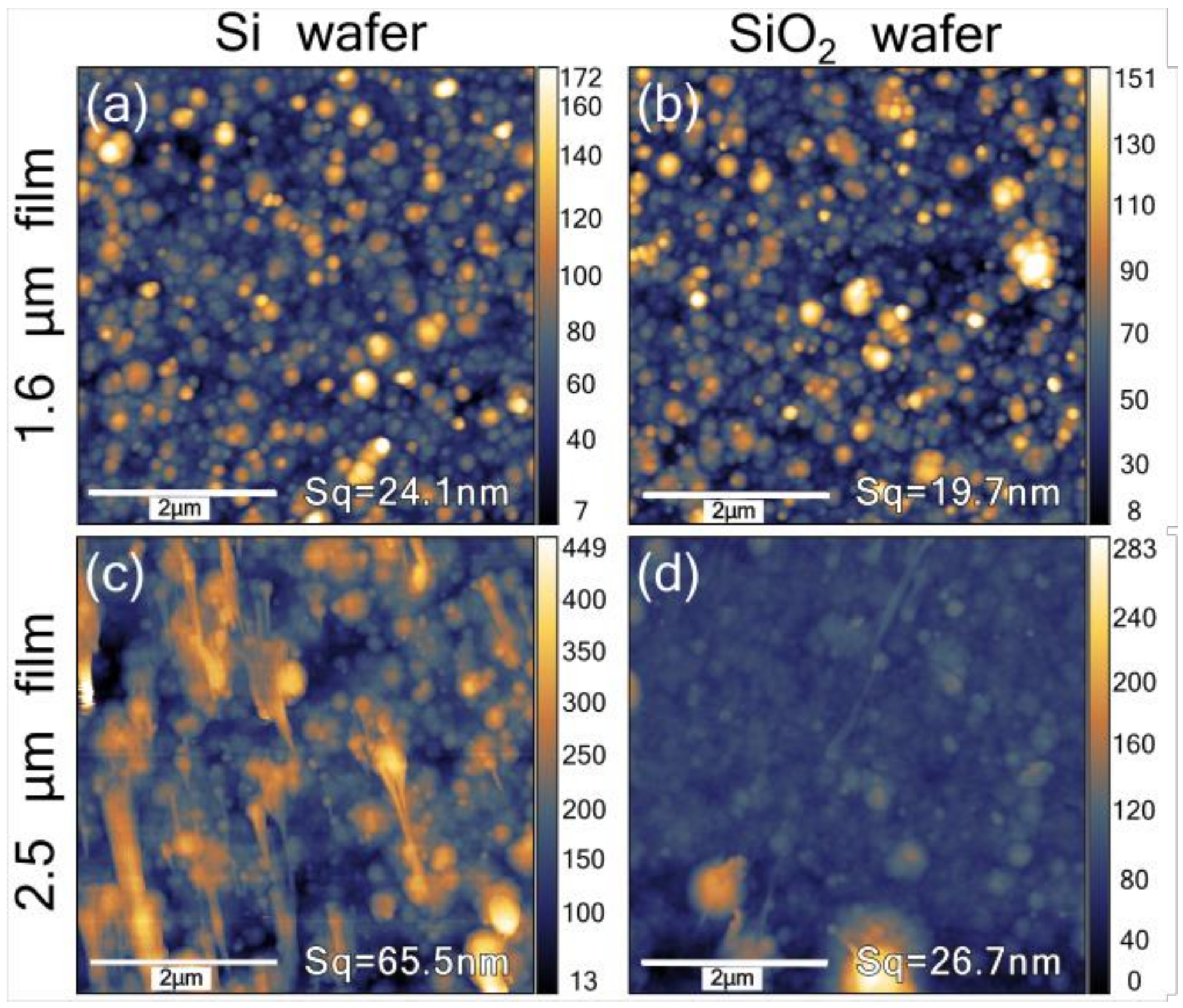
3.4. AFM Topography Measurements

The topography of the AF4 coatings was investigated to see if any differences can be observed and how the deposition process could affect the topography. Surface morphology of the AF4 coatings shows the difference between the cases of Si and SiO2 substrates as well as various film thicknesses (1.6 and 2.5 μm), which can be observed in Figure 6.
Despite the similar appearance, the 1.6 μm AF4 parylene coating on the Si wafer shows higher rms roughness than the one deposited on the SiO2 substrate by almost 25%. Similar behavior is observed for the thicker 2.5 μm films, where, however, the contrast in the roughness values is much higher, reaching up to 200%. Although the latter case shows more uniform surface, one can occasionally observe large round clusters of the polymer of about 300 nm in height. The case of the Si substrate, however, displays numerous elongated thread-like structures, which presumably originate from the polymer chains unable to recrystallize during the deposition. This is not the case for the 1.6 μm coatings. It thus suggests a certain temperature gradient within the films, leading to the disparity in the surface morphologies.
The topography is also in correspondence with the crystallinity and mechanical properties, which all suggests that the bonding property differences in the AF4 coatings come from the deposition process itself.

4. Conclusions

The pull-off F/s curves of the AF4 coatings deposited by VDP on Si and SiO2 wafers were parameterized by pull-off energy, which showed a divergence in the energies required to reach the pull-off on the AF4-Si and AF4-SiO2 samples. By only analyzing the bond strengths, a small or negligible difference was observed. The F/s curves of the AF4 coating deposited on the SiO2 substrate, in contrast to the Si substrate, showed an increased ductility with a strain hardening mechanism occurring for the AF4 coating. By nanoindentation measurements, it was shown that the elastic modulus of the AF4 coating on the SiO2 substrate was about twice as high as that of the AF4 coating on Si. Since the elastic modulus is a cohesive property of the coating, it can explain the higher pull-off energy of the AF4 coating on the SiO2 in comparison to the Si substrate. This is in accordance with our findings from [25], where it was shown that the AF4 coating delaminates mainly cohesively by pull-off testing. Adhesion of the AF4 coatings on Si and SiO2 substrates seems to be good, since the AF4 coating itself fails rather cohesively and adhesive failure is rarer. The divergence in the pull-off energies is therefore based on the divergence in the cohesive properties rather than the adhesive properties. The difference in the cohesive properties is directly correlated to the microstructure of AF4 coatings, as characterized by XRD and Raman spectroscopy. The characterization results showed that the crystallinity of the AF4 coating on SiO2 is higher than on the Si substrates owing to the stronger interaction of the polymeric chains in the earlier case, which can be explained by the higher temperature on the SiO2 substrate in comparison to the Si substrate during the film growth of the AF4 coating.
As our work shows what a high impact the deposition process and the substrate material can have on the AF4 coatings properties, it is very important to carefully design the deposition process for reaching AF4 coatings with same or similar properties, which can then be applied to harsh environments where thermal, corrosive, mechanical and UV stability must be given. MEMS, sensors or power devices with AF4 packaging coatings can be used, for example, in space, biomedical or mining applications, where the excellent AF4 properties can be decisive for a reliable working process of electronics devices.

Supplementary Materials

The following supporting information can be downloaded at: https://www.mdpi.com/article/10.3390/coatings13020237/s1, Figure S1: F/s curves of the pull-off tests on the 1.6 μm and 2.5 μm thick AF4 parylene coatings deposited on Si and SiO2 substrates; Figure S2: (a) X-ray diffraction patterns and (b) Raman spectra of the 2.5 μm parylene AF-4 films deposited on the Si and SiO2 wafers. The 2.5 μm parylene coatings exhibit similar behavior to the 1.6 μm thick ones but introduce the deviation, which is purely thickness-dependent: parylene molecules seem to polymerize less efficiently at the higher film thickness due to the temperature gradient present; Table S1: Parylene AF-4 mode assignment; Table S2: Calculation of the area ratio for the selected modes.

Author Contributions

Conceptualization, T.S., D.S. and G.M.; methodology, T.S., D.S. and G.M.; software, T.S. and D.S.; validation, T.S. and D.S.; formal analysis, T.S. and D.S.; investigation, T.S. and D.S.; resources, G.M.; data curation, T.S., D.S. and G.M.; writing—original draft preparation, T.S. and D.S.; writing—review and editing, T.S., D.S. and G.M.; visualization, T.S. and D.S.; supervision, G.M.; project administration, G.M.; funding acquisition, T.S., D.S. and G.M. All authors have read and agreed to the published version of the manuscript.

Funding

This project was performed within the COMET Centre ASSIC Austrian Smart Systems Integration Research Center, which is funded by BMK, BMDW and the Austrian provinces of Carinthia and Styria within the framework of COMET—Competence Centers for Excellent Technologies. The COMET programme is run by FFG.

Institutional Review Board Statement

This study did not require ethical approval.

Informed Consent Statement

Not applicable.

Data Availability Statement

The data presented in this study are available on request from the corresponding author.

Conflicts of Interest

The authors declare no conflict of interest. The funders had no role in the design of the study; in the collection, analyses, or interpretation of data; in the writing of the manuscript; or in the decision to publish the results.

References

  1. Kim, B.J.; Meng, E. Micromachining of parylene C for bioMEMS. Polym. Adv. Technol. 2016, 27, 564–576. [Google Scholar] [CrossRef]
  2. Tian, L.; Yin, Y.; Zhao, J.; Jin, H.; Shang, Y.; Yan, S.; Dong, S. Parylene F coatings for combating marine biofouling. Mater. Lett. 2021, 285, 129141. [Google Scholar] [CrossRef]
  3. Hassler, C.; von Metzen, R.P.; Ruther, P.; Stieglitz, T. Characterization of parylene C as an encapsulation material for implanted neural prostheses. J. Biomed. Mater. B Appl. Biomater. 2010, 93, 267–274. [Google Scholar] [CrossRef]
  4. Mariello, M.; Kim, K.; Wu, K.; Lacour, S.P.; Leterrier, Y. Recent advances in encapsulation of flexible bioelectronic implants: Materials, Technologies, and Characterization Methods. Adv. Mater. 2022, 34, 2201129. [Google Scholar] [CrossRef] [PubMed]
  5. Golda-Cepa, M.; Engvall, K.; Hakkarainen, M.; Kotarba, A. Recent progress on parylene C polymer for biomedical applications: A review. Prog. Organ. Coat. 2020, 140, 105493. [Google Scholar] [CrossRef]
  6. Zhu, J.; Liu, X.; Shi, Q.; He, T.; Sun, Z.; Guo, X.; Lee, C. Development trends and perspectives of future sensors and MEMS/NEMS. Micromachines 2020, 11, 7. [Google Scholar] [CrossRef] [Green Version]
  7. Kim, B.J.; Meng, E. Review of polymer MEMS micromachining. J. Micromech. Microeng. 2016, 26, 013001. [Google Scholar] [CrossRef]
  8. Ortigoza-Diaz, J.; Scholten, K.; Larson, C.; Cobo, A.; Hudson, T.; Yoo, J.; Meng, E. Techniques and considerations in the microfabrication of parylene c microelectromechanical systems. Micromachines 2018, 9, 422. [Google Scholar] [CrossRef] [Green Version]
  9. Selbmann, F.; Baum, M.; Meinecke, C.; Wiemer, M.; Kuhn, H.; Joseph, Y. Low-temperature parylene-based adhesive bonding technology for 150 and 200 mm wafers for fully biocompatible and highly reliable microsystems. ECS J. Solid State Sci. Technol. 2021, 10, 074010. [Google Scholar] [CrossRef]
  10. Xu, H.; Yang, Z.; Guo, Y.; Xu, Q.; Dou, S.; Jin, Y.; Wang, W. Copolymerization of Parylene C and Parylene F to Enhance Adhesion and Thermal Stability without Coating Performance Degradation; SSRN: Rochester, NY, USA, 2022; pp. 1–14. Available online: https://ssrn.com/abstract=4259971 (accessed on 15 January 2023).
  11. Seymour, J.P.; Elkasabi, Y.M.; Chen, H.Y.; Lahann, J.; Kipke, D.R. The insulation performance of reactive parylene films in implantable electronic devices. Biomaterials 2009, 30, 6158–6167. [Google Scholar] [CrossRef]
  12. Hartmann, F.; Jakešová, M.; Mao, G.; Nikić, M.; Kaltenbrunner, M.; Đerek, V.; Głowacki, E.D. Scalable microfabrication of folded parylene-based conductors for stretchable electronics. Adv. Electron. Mater. 2021, 7, 2001236. [Google Scholar] [CrossRef]
  13. Xie, X.; Rieth, L.; Merugu, S.; Tathireddy, P.; Solzbacher, F. Plasma-assisted atomic layer deposition of Al2O3 and parylene C bi-layer encapsulation for chronic implantable electronics. Appl. Phys. Lett. 2012, 101, 093702. [Google Scholar] [CrossRef] [PubMed] [Green Version]
  14. Marszalek, T.; Gazicki-Lipman, M.; Ulanski, J. Parylene C as a versatile dielectric material for organic field-effect transistors. Beilstein J. Nanotechnol. 2017, 8, 1532–1545. [Google Scholar] [CrossRef] [PubMed] [Green Version]
  15. Trantidou, T.; Tariq, M.; Terracciano, C.M.; Toumazou, C.; Prodromakis, T. Parylene C-based flexible electronics for ph monitoring applications. Sensors 2014, 14, 11629–11639. [Google Scholar] [CrossRef] [PubMed] [Green Version]
  16. Qiu, Y.; Jung, Y.H.; Lee, S.; Shih, T.Y.; Lee, J.; Xu, Y.H.; Ma, Z. Compact parylene-c-coated flexible antenna for WLAN and upper-band UWB applications. Electron. Lett. 2014, 50, 1782–1784. [Google Scholar] [CrossRef]
  17. Buchwalder, S.; Borzì, A.; Diaz Leon, J.J.; Bourgeois, F.; Nicolier, C.; Nicolay, S.; Burger, J. Thermal analysis of parylene thin films for barrier layer applications. Polymers 2022, 14, 3677. [Google Scholar] [CrossRef]
  18. Kahouli, A.; Sylvestre, A.; Jomni, F.; André, E.; Garden, J.L.; Yangui, B.; Legrand, J. Dielectric properties of parylene AF4 as low-k material for microelectronic applications. Thin Solid Films 2012, 520, 2493–2497. [Google Scholar] [CrossRef]
  19. Dolbier, W.R., Jr.; Beach, W.F. Parylene-AF4: A polymer with exceptional dielectric and thermal properties. J. Fluorine Chem. 2003, 122, 97–104. [Google Scholar] [CrossRef]
  20. Hicks, C.; Duffy, B.; Hargaden, G.C. Synthesis and modification of octafluoro [2.2] paracyclophane (parylene AF4). Org. Chem. Front. 2014, 1, 716–725. [Google Scholar] [CrossRef] [Green Version]
  21. Senkovich, J.J. Parylene AF-4 via the trapping of a phenoxy leaving group. Chem. Vapor. Depos. 2013, 19, 327–331. [Google Scholar] [CrossRef]
  22. Lagomarsini, C.; Jean-Mistral, C.; Kachroudi, A.; Monfray, S.; Sylvestre, A. Outstanding performance of parylene polymers as electrets for energy harvesting and high-temperature applications. J. Appl. Polym. Sci. 2019, 137, 48790. [Google Scholar] [CrossRef]
  23. Karakurt, I.; Zhong, J.; Lin, L. 3D printed flexible triboelectric energy harvesters via conformal coating of parylene AF4. In Proceedings of the 32nd international conference on micro electro mechanical systems (MEMS), Seoul, Republic of Korea, 27–31 January 2019. [Google Scholar]
  24. Watson, A.M.; Dease, K.; Terrab, S.; Roath, C.; Gopinath, J.T.; Bright, V.M. Focus-tunable low-power electrowetting lenses with thin parylene films. Appl. Opt. 2015, 54, 6224–6229. [Google Scholar] [CrossRef] [PubMed] [Green Version]
  25. Sinani, T.; Miskovic, G. Adhesion evaluation of parylene AF4 to silicon and glass substrate. In Proceedings of the 45th international spring seminar on electronics technology (ISSE), Vienna, Austria, 11–15 May 2022; pp. 1–6. [Google Scholar]
  26. Vencl, A.; Arostegui, S.; Favaro, G.; Zivic, F.; Mrdak, M.; Mitrović, S.; Popovic, V. Evaluation of adhesion/cohesion bond strength of the thick plasma spray coatings by scratch testing on coatings cross-sections. Tribol. Int. 2011, 44, 1281–1288. [Google Scholar] [CrossRef]
  27. Sickfeld, J. Pull-off test, an internationally standardized method for adhesion testing-assessment of the relevance of test results. In Adhesion Aspects of Polymeric Coatings; Springer: Boston, MA, USA, 1983; pp. 543–567. [Google Scholar]
  28. Awaja, F.; Gilbert, M.; Kelly, G.; Fox, B.; Pigram, P.J. Adhesion of polymers. Prog. Polymer Sci. 2009, 34, 948–968. [Google Scholar] [CrossRef]
  29. Harder, T.A.; Yao, T.J.; He, Q.; Shih, C.Y.; Tai, Y.C. Residual stress in thin-film parylene-C. In Proceedings of the MEMS IEEE international conference, Las Vegas, NV, USA, 24 January 2002. [Google Scholar]
  30. Ramos, N.M.; Simões, M.L.; Delgado, J.M.; Freitas, V.P.D. Applicability of the pull-off test: Teachings from a large sample of in situ tests. In Hygrothermal Behavior, Building Pathology and Durability; Springer: Berlin/Heidelberg, Germany, 2013; pp. 165–181. [Google Scholar]
  31. Goodno, B.J.; Gere, J.M. Mechanics of Materials; Cengage Learning: Boston, MA, USA, 2020. [Google Scholar]
  32. Hsu, J.M.; Rieth, L.; Kammer, S.; Orthner, M.; Solzbacher, F. Effect of thermal and deposition processes on surface morphology, crystallinity, and adhesion of Parylene-C. Sens. Mater. 2008, 20, 87–102. [Google Scholar]
  33. Song, Z.; Park, J.H.; Kim, H.R.; Lee, G.Y.; Kang, M.J.; Kim, M.H.; Pyun, J.C. Carbon electrode obtained via pyrolysis of plasma-deposited parylene-c for electrochemical immunoassays. Analyst 2022, 147, 3783–3794. [Google Scholar] [CrossRef]
  34. Ramaswamy, S.; Gleason, K.K. Overview of strategies for the cvd of organic films and functional polymer layers. Chem. Vapor Depos. 2009, 15, 77–90. [Google Scholar]
  35. Mihály, J.; Sterkel, S.; Ortner, H.M.; Kocsis, L.; Hajba, L.; Furdyga, É.; Mink, J. FTIR and FT-Raman spectroscopic study on polymer based high pressure digestion vessels. Croat. Chem. Acta 2006, 79, 5. [Google Scholar]
  36. Solonenko, D.; Gasiorowski, J.; Apaydin, D.; Oppelt, K.; Nuss, M.; Keawsongsaeng, W.; Thamyongkit, P. Doping-induced polaron formation and solid-state polymerization in benzoporphyrin-oligothiophene conjugated systems. J. Phys. Chem. C 2017, 121, 24397–24407. [Google Scholar] [CrossRef]
Figure 1. (a) Chemical structure of parylene AF4 and (b) the Gorham process presented in three steps for depositing AF4 coatings.
Coatings 13 00237 g001
Figure 2. Schematic representation of a pull-off F/s curve.
Coatings 13 00237 g002
Figure 3. (a) Bond strengths and (b) pull-off energies for the different AF4 coatings presented in graphs from the data in Table 1.
Coatings 13 00237 g003aCoatings 13 00237 g003b
Figure 4. Data from Table 2. Presented in graphs.
Coatings 13 00237 g004
Figure 5. (Left) X-ray diffraction patterns and (right) Raman spectra of the 1.6 μm parylene AF4 films deposited on the Si and SiO2 substrates.
Coatings 13 00237 g005
Figure 6. Surface morphology images of the 1.6 μm AF4 coating on Si (a) and SiO2 (b) substrates and 2.5 μm AF4 films deposited on Si (c) and SiO2 (d) substrates obtained via atomic force microscopy. The rms surface roughness, Sq, is given in the corresponding images.
Coatings 13 00237 g006
Table 1. Bond strength and pull-off energy results for all the investigated AF4 coatings by pull-off testing.
Sample TypeBond Strength [kPa]Pull-Off Energy [mJ]
Si substrate-1.6 μm AF4220 ± 88 kPa1.4 ± 0.5 mJ
Si substrate-2.5 μm AF4234 ± 85 kPa1.7 ± 0.8 mJ
SiO2 substrate-1.6 μm AF4303 ± 82 kPa3.0 ± 1.0 mJ
SiO2 substrate-2.5 μm AF4240 ± 55 kPa6.3 ± 1.8 mJ
Table 2. Nanoindentation elastic modulus results for the AF4 coatings.
Sample TypeElastic Modulus [GPa]
Si substrate-1.6 μm AF43.2 ± 0.4 GPa
Si substrate-2.5 μm AF43.8 ± 0.4 GPa
SiO2 substrate-1.6 μm AF45.8 ± 1.0 GPa
SiO2 substrate-2.5 μm AF47.7 ± 2.0 GPa
Disclaimer/Publisher’s Note: The statements, opinions and data contained in all publications are solely those of the individual author(s) and contributor(s) and not of MDPI and/or the editor(s). MDPI and/or the editor(s) disclaim responsibility for any injury to people or property resulting from any ideas, methods, instructions or products referred to in the content.

