
Controlling of Chemical Bonding Structure, Wettability, Optical Characteristics of SiCN:H (SiC:H) Films Produced by PECVD Using Tetramethylsilane and Ammonia Mixture


Abstract
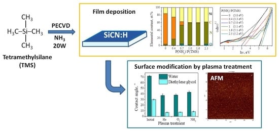
:
1. Introduction
2. Materials and Methods
2.1. Materials
2.2. PECVD and Surface Modification
2.3. Plasma Characterization
2.4. Characterization of Chemical Bonding Structure and Composition
2.5. Characterization of Thickness and Optical Properties
2.6. Surface Topology
2.7. Wettability and Free Surface Energy
3. Results and Discussion
3.1. Effect of Deposition Temperature during the PECVD Process
3.2. Variation of NH3 Concentration in Initial Gas Mixture
3.3. Surface Modification by He, O2, NH3 Plasma
4. Conclusions
Author Contributions
Funding
Institutional Review Board Statement
Informed Consent Statement
Data Availability Statement
Acknowledgments
Conflicts of Interest
References
- Sha, B.; Lukianov, A.N.; Dusheiko, M.G.; Lozinskii, V.B.; Klyui, A.N.; Korbutyak, D.V.; Pritchin, S.E.; Klyui, N.I. Carbon-rich amorphous silicon carbide and silicon carbonitride films for silicon-based photoelectric devices and optical elements: Application from UV to mid-IR spectral range. Opt. Mater. 2020, 106, 109959. [Google Scholar] [CrossRef]
- Khatami, Z.; Bleczewski, L.; Neville, J.J.; Mascher, P. X-ray Absorption Spectroscopy of Silicon Carbide Thin Films Improved by Nitrogen for All-Silicon Solar Cells. ECS J. Solid State Sci. Technol. 2020, 9, 083002. [Google Scholar] [CrossRef]
- Khatami, Z.; Nowikow, C.; Wojcik, J.; Mascher, P. Annealing of silicon carbonitride nanostructured thin films: Interdependency of hydrogen content, optical, and structural properties. J. Mater. Sci. 2018, 53, 1497–1513. [Google Scholar] [CrossRef]
- Chou, T.H.; Kuo, T.W.; Lin, C.Y.; Lai, F.S. A low cost n-SiCN/p-PS/p-Si heterojunction for high temperature ultraviolet detecting applications. Sens. Actuators A Phys. 2018, 279, 462–466. [Google Scholar] [CrossRef]
- Plujat, B.; Glénat, H.; Hamon, J.; Gazal, Y.; Goullet, A.; Hernandez, E.; Quoizola, S.; Thomas, L. Near-field scanning microscopy and physico-chemical analysis versus time of SiCN:H thin films grown in Ar/NH3/TMS gas mixture using MW-Plasma CVD at 400 °C. Plasma Process. Polym. 2018, 15, 1800066. [Google Scholar] [CrossRef]
- Rumyantsev, Y.M.; Chagin, M.N.; Shayapov, V.R.; Yushina, I.V.; Kichai, V.N.; Kosinova, M.L. Synthesis and Properties of Thin Films Formed by Vapor Deposition from Tetramethylsilane in a Radio-Frequency Inductively Coupled Plasma Discharge. Glass Phys. Chem. 2018, 44, 174–182. [Google Scholar] [CrossRef]
- Zhuang, C.; Schlemper, C.; Fuchs, R.; Zhang, L.; Huang, N.; Vogel, M.; Staedler, T.; Jiang, X. Mechanical behavior related to various bonding states in amorphous Si–C–N hard films. Surf. Coat. Technol. 2014, 258, 353. [Google Scholar] [CrossRef]
- Fainer, N.I.; Kosinova, M.L.; Rumyantsev, Y.M.; Maximovskii, E.A.; Kuznetsov, F.A. Thin silicon carbonitride films are perspective low-k materials. J. Phys. Chem. Solids 2008, 69, 661. [Google Scholar] [CrossRef]
- Szymanowski, H.; Olesko, K.; Kowalski, J.; Fijalkowski, M.; Gazicki-Lipman, M.; Sobczyk-Guzenda, A. Thin SiNC/SiOC Coatings with a Gradient of Refractive Index Deposited from Organosilicon Precursor. Coatings 2020, 10, 794. [Google Scholar] [CrossRef]
- Wrobel, A.M.; Blaszczyk-Lezak, I. Remote Hydrogen Microwave Plasma CVD of Silicon Carbonitride Films from a Tetramethyldisilazane Source. Part 2: Compositional and Structural Dependencies of Film Properties. Chem. Vap. Depos. 2007, 13, 595–600. [Google Scholar] [CrossRef]
- Guruvenket, S.; Andrie, S.; Simon, M.; Johnson, K.W.; Sailer, R.A. Atmospheric-Pressure Plasma-Enhanced Chemical Vapor Deposition of a-SiCN:H Films: Role of Precursors on the Film Growth and Properties. Appl. Mater. Interfaces 2012, 4, 5293–5299. [Google Scholar] [CrossRef] [PubMed]
- Fainer, N.I. From organosilicon precursors to multifunctional silicon carbonitride. Russ. J. Gen. Chem. 2012, 82, 43–52. [Google Scholar] [CrossRef]
- Ermakova, E.; Lis, A.; Kosinova, M.; Rumyantsev, Y.; Maximovskii, E.; Rakhlin, V. Bis(trimethylsilyl)ethylamine: Synthesis, properties and its use as CVD precursor. Phys. Proc. 2013, 46, 209–218. [Google Scholar] [CrossRef] [Green Version]
- Ermakova, E.; Mogilnikov, K.; Asanov, I.; Fedorenko, A.; Yushina, I.; Kichay, V.; Maksimovskiy, E.; Kosinova, M. Chemical Structure, Optical and Dielectric Properties of PECVD SiCN Films Obtained from Novel Precursor. Coatings 2022, 12, 1767. [Google Scholar] [CrossRef]
- Cheng, Y.-L.; Lin, Y.-L. Comparison of SiCxNy barriers using different deposition precursors capped on porous low-dielectric-constant SiOCH dielectric film. Thin Solid Films 2020, 702, 137983. [Google Scholar] [CrossRef]
- Ma, X.; Xu, C.; Mao, Z.; Ji, P.; Jin, C.; Xu, D.; Ding, Y. Synthesis, characterization, and thermal properties of novel silicon 1,1,3,3-tetramethylguanidinate derivatives and use as single-source chemical vapor deposition precursors. Appl. Organomet. Chem. 2020, 34, e5349. [Google Scholar] [CrossRef]
- Wrobel, A.M.; Uznanski, P. Hard silicon carbonitride thin-film coatings by remote hydrogen plasma chemical vapor deposition using aminosilane and silazane precursors. 2: Physical, optical, and mechanical properties of deposited films. Plasma Process. Polym. 2021, 18, 2000241. [Google Scholar] [CrossRef]
- Ng, Y.M.; Ong, C.W.; Zhao, X.A.; Choy, C.L. Polymerization of dual ion beam deposited CNx films with increasing N content. Vacuum Sci. Technol. 1999, 17, 584. [Google Scholar] [CrossRef]
- Fainer, N.I.; Plekhanov, A.G.; Golubenko, A.N.; Rumyantsev, Y.M.; Rakhlin, V.I.; Maximovski, E.A.; Shayapov, V.R. PECVD Synthesis of Silicon Carbonitride Layers Using Methyltris(diethylamino)silane as the New Single-Source Precursor. J. Solid State Sci. Technol. 2015, 4, N3153. [Google Scholar] [CrossRef]
- Fainer, N.I.; Golubenko, A.N.; Rumyantsev, Y.M.; Kesler, V.G.; Ayupov, B.M.; Rakhlin, V.I.; Voronkov, M.G. Tris(diethylamino)silane—A new precursor compound for obtaining layers of silicon carbonitride. Glass Phys. Chem. 2012, 38, 15. [Google Scholar] [CrossRef]
- Wrobel, A.M.; Blaszczyk-Lezak, I.; Uznanski, P.; Glebocki, B. Remote Hydrogen Microwave Plasma Chemical Vapor Deposition of Amorphous Silicon Carbonitride (a-SiCN) Coatings Derived from Tris (dimethylamino) Silane. Plasma Process. Polym. 2011, 8, 542. [Google Scholar] [CrossRef]
- Zhou, Y.; Probst, D.; Thissen, A.; Kroke, E.; Riedel, R.; Hauser, R.; Hoche, H.; Broszeit, E.; Kroll, P.; Stafast, H. Hard silicon carbonitride films obtained by RF-plasma-enhanced chemical vapour deposition using the single-source precursor bis(trimethylsilyl)carbodiimide. J. Eur. Ceram. Soc. 2006, 26, 1325–1335. [Google Scholar] [CrossRef]
- Smirnova, T.P.; Badalyan, A.M.; Yakovkina, L.V.; Sysoeva, N.H.; Asanov, I.P.; Kaichev, V.V.; Bukhtiarov, V.I.; Shmakov, A.N. Silicon carbonitride films synthesized from new sources. Chem. Sustain. Dev. 2001, 9, 23–29. [Google Scholar]
- Ermakova, E.; Kosinova, M. Organosilicon compounds as single-source precursors for SiCN films production. J. Organomet. Chem. 2022, 958, 122183. [Google Scholar] [CrossRef]
- Beake, B.D.; McMaster, S.J.; Liskiewicz, T.W. Contact size effects on the friction and wear of amorphous carbon films. Appl. Surf. Sci. Adv. 2022, 9, 100248. [Google Scholar] [CrossRef]
- Maruno, H.; Nishimoto, A. Adhesion and durability of multi-interlayered diamond-like carbon films deposited on aluminum alloy. Surf. Coat. Technol. 2018, 354, 134–144. [Google Scholar] [CrossRef]
- Nishikawa, J.; Sugihara, N.; Nakano, M.; Hieda, J.; Ohtake, N.; Akasaka, H. Effect of Si incorporation on corrosion resistance of hydrogenated amorphous carbon film. Diamond Relat. Mater. 2018, 90, 207–213. [Google Scholar] [CrossRef]
- Wu, H.Y.; Hsu, C.H.; Liu, T.X.; Ou, Y.C.; Hsu, Y.H.; Wu, W.Y.; Lien, S.Y.; Jiang, Y.L. Silicon nitride cover layer prepared by silane-free plasma chemical vapor deposition for high quality surface passivation of silicon solar cells. Surf. Coat. Technol. 2019, 376, 68–73. [Google Scholar] [CrossRef]
- Plujat, B.; Glénat, H.; Bousquet, A.; Frézet, L.; Hamon, J.; Goullet, A.; Tomasella, E.; Hernandez, E.; Quoizola, S.; Thomas, L. SiCN:H thin films deposited by MW-PECVD with liquid organosilicon precursor: Gas ratio influence versus properties of the deposits. Plasma Process. Polym. 2020, 17, 1900138. [Google Scholar] [CrossRef]
- Silva, J.A.; Quoizola, S.; Hernandez, E.; Thomas, L.; Massines, F. Silicon carbon nitride films as passivation and antireflective coatings for silicon solar cells. Surf. Coat. Technol. 2014, 242, 157–163. [Google Scholar] [CrossRef]
- Soum-Glaude, A.; Bousquet, I.; Thomas, L.; Flamant, G. Optical modeling of multilayered coatings based on SiC(N)H materials for their potential use as high-temperature solar selective absorbers. Sol. Energy Mater. Sol. Cells 2013, 117, 315–323. [Google Scholar] [CrossRef]
- Chen, S.-W.; Wang, Y.-S.; Hu, S.-Y.; Lee, W.-H.; Chi, C.-C.; Wang, Y.-L. A Study of Trimethylsilane (3MS) and Tetramethylsilane (4MS) Based α-SiCN:H/α-SiCO:H Diffusion Barrier Films. Materials 2012, 5, 377–384. [Google Scholar] [CrossRef] [PubMed]
- Pech, D.; Schupp, N.; Steyer, P.; Hack, T.; Gachon, Y.; Héau, C.; Loir, A.S.; Sánchez-López, J.C. Duplex SiCN/DLC coating as a solution to improve fretting—Corrosion resistance of steel. Wear 2009, 266, 832–838. [Google Scholar] [CrossRef]
- Ermakova, E.N.; Rumyantsev, Y.M.; Rakhlin, V.I.; Kosinova, M.L. Plasma-chemical synthesis of transparent dielectric Si–C–O–H films from trimethylphenoxysilane. High Energy Chem. 2016, 50, 224–227. [Google Scholar] [CrossRef]
- Kramida, A.; Ralchenko, Y.; Reader, J. NIST ASD Team; National Institute of Standards and Technology: Gaithersburg, MD, USA, 2022. Available online: https://search.datacite.org/works/10.18434/t4w30f (accessed on 15 October 2022).
- Cui, J.H.; Xu, Z.F.; Zhang, J.L.; Nie, Q.Y.; Xu, G.H.; Ren, L.L. Online diagnosis of electron excitation temperature in CH4+H2 discharge plasma at atmospheric pressure by optical emission spectra. Sci. China Ser. G Phys. Mech. Astron 2008, 51, 1892–1896. [Google Scholar] [CrossRef]
- Tauc, J.; Grigorovici, R.; Vancu, A. Optical Properties and Electronic Structure of Amorphous Germanium. Phys. Stat. Sol. B 1966, 15, 627–637. [Google Scholar] [CrossRef]
- Kwok, D.Y.; Neumann, A.W. Contact angle measurements and contact angle interpretation. Adv. Colloid Interface Sci. 1999, 81, 167. [Google Scholar] [CrossRef]
- Owens, D.K.; Wendt, R.C. Estimation of the surface free energy of polymers. J. Appl. Polym. Sci. 1969, 13, 1741–1747. [Google Scholar] [CrossRef]
- Wu, S. Polymer Interface and Adhesion; Marcel Dekker: New York, NY, USA, 1982; ISBN 9780824715335. [Google Scholar]
- Ivashchenko, V.I.; Porada, O.K.; Kozak, A.O.; Manzhara, V.S.; Sinelnichenko, O.K.; Ivashchenko, L.A.; Shevchenko, R.V. An effect of hydrogenation on the photoemission of amorphous SiCN films. Int. J. Hydrogen Energy 2022, 47, 7263–7273. [Google Scholar] [CrossRef]
- Matsutani, T.; Tai, Y.; Kawasaki, T. Nitrogen ion beam thinning of a-SiCN diaphragm for environmental cell prepared by low-energy ion beam enhanced chemical vapor deposition. Vacuum 2020, 182, 109770. [Google Scholar] [CrossRef]
- Long, D.A. Tables and Charts. In Infrared and Raman Characteristic Group Frequencies, 3rd ed.; John Wiley and Sons: Hoboken, NJ, USA; George Socrates: Chichester, UK, 2001. [Google Scholar] [CrossRef]
- Langford, A.A.; Fleet, M.L.; Nelson, B.P.; Lanford, W.A.; Maley, N. Infrared absorption strength and hydrogen content of hydrogenated amorphous silicon. Phys. Rev. B 1992, 45, 13367. [Google Scholar] [CrossRef] [PubMed]
- Chagin, M.N.; Sulyaeva, V.S.; Shayapov, V.R.; Kolodin, A.N.; Khomyakov, M.N.; Yushina, I.V.; Kosinova, M.L. Synthesis, Properties and Aging of ICP-CVD SiCxNy:H Films Formed from Tetramethyldisilazane. Coatings 2022, 12, 80. [Google Scholar] [CrossRef]
- Kafrouni, W.; Rouessac, V.; Julbe, A.; Durand, J. Synthesis and characterization of silicon carbonitride films by plasma enhanced chemical vapor deposition (PECVD) using bis(dimethylamino)dimethylsilane (BDMADMS), as membrane for a small molecule gas separation. Appl. Surf. Sci. 2010, 257, 1196–1203. [Google Scholar] [CrossRef]
- Wrobel, A.M.; Uznanski, P.; Walkiewicz-Pietrzykowska, A.; Jankowski, K. Amorphous silicon carbonitride thin-film coatings produced by remote nitrogen microwave plasma chemical vapour deposition using organosilicon precursor. Appl. Organomet. Chem. 2017, 31, e3871. [Google Scholar] [CrossRef]
- Khatami, Z.; Bosco, G.B.F.; Wojcik, J.; Tessler, L.R.; Mascher, P. Influence of Deposition Conditions on the Characteristics of Luminescent Silicon Carbonitride Thin Films. ECS J. Solid State Sci. Technol. 2018, 7, N7. [Google Scholar] [CrossRef] [Green Version]
- Khatami, Z.; Mascher, P. Photoluminescence of silicon carbonitride thin films: The interdependence of post-deposition annealing and growth temperature. J. Lumin. 2019, 214, 116563. [Google Scholar] [CrossRef]
- Uznanski, P.; Walkiewicz-Pietrzykowska, A.; Jankowski, K.; Zakrzewska, J.; Wrobel, A.M.; Balcerzak, J.; Tyczkowski, J. Atomic Hydrogen Induced Chemical Vapor Deposition of Silicon Oxycarbide Thin Films Derived from Diethoxymethylsilane Precursor. Appl. Organomet. Chem. 2020, 34, e5674. [Google Scholar] [CrossRef]
- Veres, M.; Koós, M.; Tóth, S.; Füle, M.; Pócsik, I.; Tóth, A.; Mohai, M.; Bertóti, I. Characterisation of a-C:H and oxygen-containing Si:C:H films by Raman spectroscopy and XPS. Diamond Relat. Mater. 2005, 14, 1051–1056. [Google Scholar] [CrossRef]
- Sobczyk-Guzenda, A.; Oleśko, K.; Gazicki-Lipman, M.; Szymański, W.; Balcerzak, J.; Wendler, B.; Szymanowski, H. Chemical structure and optical properties of a-SiNC coatings synthesized from different disilazane precursors with the RF plasma enhanced CVD technique—A comparative study. Mater. Res. Express 2019, 6, 016410. [Google Scholar] [CrossRef]
- Chang, W.Y.; Chang, C.Y.; Leu, J. Optical properties of plasma-enhanced chemical vapor deposited SiCxNy films by using silazane precursors. Thin Solid Films 2017, 636, 671–679. [Google Scholar] [CrossRef]
- Belmahi, M.; Bulou, S.; Thouvenin, A.; Poucques, L.; Hugon, R.; Brizoual, L.; Miska, P.; Genève, D.; Vasseur, J.L.; Bougdira, J. Microwave plasma process for SiCN:H thin films synthesis with composition varying from SiC:H to SiN:H in H2/N2/Ar/Hexamethyldisilazane gas mixture. Plasma Process. Polym. 2014, 11, 551–558. [Google Scholar] [CrossRef]
- Sinha, A.K.; Lugujjo, E. Lorentz-Lorenz correlation for reactively plasma deposited Si-N films. Appl. Phys. Lett. 1978, 32, 245. [Google Scholar] [CrossRef]
- Swanepoel, R. Determination of the thickness and optical constants of amorphous silicon. J. Phys. E Sci. Instrum. 1983, 16, 1214. [Google Scholar] [CrossRef] [Green Version]
- Bachar, A.; Bousquet, A.; Mehdi, H.; Monier, G.; Robert-Goumet, C.; Thomas, L.; Belmahi, M.; Goullet, A.; Sauvage, T.; Tomasella, E. Composition and optical properties tunability of hydrogenated silicon carbonitride thin films deposited by reactive magnetron sputtering. App. Surf. Sci. 2018, 444, 293–302. [Google Scholar] [CrossRef]
- Saito, N.; Goto, T.; Tomioka, Y.; Yamaguchi, T. Improvement of photoconductivity of a-SiC:H films by introducing nitrogen during magnetron sputtering process. J. Appl. Phys. 1991, 69, 1518–1521. [Google Scholar] [CrossRef]
- Kozak, A.O.; Ivashchenko, V.I.; Porada, O.K.; Ivashchenko, L.A.; Tomila, T.V.; Manjara, V.S.; Klishevych, G.V. Structural, optoelectronic and mechanical properties of PECVD Si–C–N films: An effect of substrate bias. Mater. Sci. Semicond. Process. 2018, 88, 65–72. [Google Scholar] [CrossRef]
- Nguyen, H.H.; Jayapal, R.; Dang, N.S.; Nguyen, V.D.; Trinh, T.T.; Jang, K.; Yi, J. Investigation of charge storage and retention characteristics of silicon nitride in NVM based on InGaZnO channels for system-on-panel applications. Microelectron. Eng. 2012, 98, 34–40. [Google Scholar] [CrossRef]
- Honda, K.; Yoshinaga, K.; Nagata, Y. Amorphous Carbon-Based Semiconductor Capable of Controlling Its Optical Gap and Conductivity by Incorporating Silicon and Nitrogen Atoms. ECS J. Solid State Sci. Technol. 2016, 5, P590. [Google Scholar] [CrossRef]
- Rossi, D.; Landers, R.; Bortoleto, J.R.R.; Durrant, S.F. Characterization of PECVD a-C:H:Si:O:Cl films. J. Vac. Sci. Technol. A 2017, 35, 04D103. [Google Scholar] [CrossRef]
- Wrobel, A.M.; Walkiewicz-Pietrzykowska, A.; Uznanski, P.; Glebocki, B. a-SiC:H Films by Remote Hydrogen Microwave Plasma CVD From Ethylsilane Precursors. Chem. Vap. Depos. 2013, 19, 242–250. [Google Scholar] [CrossRef]
- Nogueira, S.; da Silva, M.L.P.; Tan, I.H.; Furlan, R. Production of hylhtly hydrophobic films using low-frequency and high density plasma. Rev. Bras. De Apl. De Vácuo 2006, 25, 45. [Google Scholar]
- Batocki, R.G.S.; Mota, R.P.; Honda, R.Y.; Santos, D.C.R. Amorphous silicon carbonitride films modified by plasma immersion ion implantation. Vacuum 2014, 107, 174–177. [Google Scholar] [CrossRef]
- Bhaskar, N.; Sulyaeva, V.; Gatapova, E.; Kaichev, V.; Rogilo, D.; Khomyakov, M.; Kosinova, M.; Basu, B. SiCxNyOz coatings enhance endothelialisation, bactericidal and reduce blood cell activation. ACS Biomater. Sci. Eng. 2020, 6, 5571–5587. [Google Scholar] [CrossRef]
- Mora-Cortes, L.F.; Rivas-Muñoz, A.N.; Neira-Velázquez, M.G.; Contreras-Esquivel, J.C.; Roger, P.; Mora-Cura, Y.N.; Soria-Arguello, G.; Bolaina-Lorenzo, E.D.; Reyna-Martínez, R.; Zugasti-Cruz, A.; et al. Biocompatible enhancement of poly (ethylene terephthalate) (PET) waste films by cold plasma aminolysis. J. Chem. Technol. Biotechnol. 2022, 97, 3001–3010. [Google Scholar] [CrossRef]
- Choi, Y.; Tran, H.-V.; Lee, T.R. Self-Assembled Monolayer Coatings on Gold and Silica Surfaces for Antifouling Applications: A Review. Coatings 2022, 12, 1462. [Google Scholar] [CrossRef]
- Zhu, L.; Dikin, D.A.; Percec, S.; Ren, F. Improving Interlayer Adhesion of Poly(p-phenylene terephthalamide) (PPTA)/Ultra-high-molecular-weight Polyethylene (UHMWPE) Laminates Prepared by Plasma Treatment and Hot Pressing Technique. Polymers 2021, 13, 2600. [Google Scholar] [CrossRef]
- Hegemann, D.; Brunner, H.; Oehr, C. Plasma treatment of polymers for surface and adhesion improvement. Nucl. Instrum. Methods Phys. Res. B 2003, 208, 281–286. [Google Scholar] [CrossRef]
- Urbanowicz, A.M.; Shamiryan, D.; Zaka, A.; Verdonck, P.; De Gendt, S.; Baklanov, M.R. Effects of He Plasma Pretreatment on Low-k Damage during Cu Surface Cleaning with NH3 Plasma. J. Electrochem. Soc. 2010, 157, H565. [Google Scholar] [CrossRef]
- Shayapov, V.R.; Chagin, M.N.; Kolodin, A.N.; Kosinova, M.L. Deposition of Films from a Mixture of Hexamethylcyclotrisilazane Vapor and Argon in Inductively Coupled Plasma. Glass Phys. Chem. 2019, 45, 525–531. [Google Scholar] [CrossRef]
- Racka-Szmidt, K.; Stonio, B.; Żelazko, J.; Filipiak, M.; Sochacki, M. A Review: Inductively Coupled Plasma Reactive Ion Etching of Silicon Carbide. Materials 2022, 15, 123. [Google Scholar] [CrossRef]
- Kumar, D.; Swain, B.P. Investigation of structural and mechanical properties of silicon carbonitride thin films. J. Alloys Compd. 2019, 789, 295. [Google Scholar] [CrossRef]
- Zhang, C.; Qu, L.; Yuan, W. Effects of Si/C Ratio on the Phase Composition of Si-C-N Powders Synthesized by Carbonitriding. Materials 2020, 13, 346. [Google Scholar] [CrossRef] [PubMed] [Green Version]
- Gray, R.C.; Carver, J.C.; Hercules, D.M. An ESCA study of organosilicon compounds. J. Electron. Spectros. Relat. Phenom. 1976, 8, 343–357. [Google Scholar] [CrossRef]
- Vassallo, E.; Cremona, A.; Ghezzi, F.; Dellera, F.; Laguardia, L.; Ambrosone, G.; Coscia, U. Structural and optical properties of amorphous hydrogenated silicon carbonitride films produced by PECVD. Appl. Surf. Sci. 2006, 252, 7993–8000. [Google Scholar] [CrossRef]
- Peng, L.; Kim, S.W.; Iacovo, S.; Inoue, F.; Phommahaxay, A.; Sleeckx, E.; De Vos, J.; Zinner, D.; Wagenleitner, T.; Uhrmann, T.; et al. Advances in SiCN-SiCN Bonding with High Accuracy Wafer-to-Wafer (W2W) Stacking Technology. In Proceedings of the 2018 IEEE International Interconnect Technology Conference (IITC), Santa Clara, CA, USA, 4–7 June 2018; pp. 179–181. [Google Scholar] [CrossRef]
- Son, S.; Min, J.; Jung, E.; Kim, H.; Kim, T.; Jeon, H.; Kim, J.; Kim, S.; Moon, K.; Na, H.; et al. Characteristics of Plasma-activated Dielectric Film Surfaces for Direct Wafer Bonding. In Proceedings of the 2020 IEEE 70th Electronic Components and Technology Conference (ECTC), Orlando, FL, USA, 3–30 June 2020; pp. 2025–2032. [Google Scholar] [CrossRef]
- Ghosh, H.; Mitra, S.; Saha, H.; Datta, S.K.; Banerjee, C. Argon plasma treatment of silicon nitride (SiN) for improved antireflection coating on c-Si solar cells. Mater. Sci. Eng. B 2017, 215, 29–36. [Google Scholar] [CrossRef]
- Li, D.; Xu, K.; Zhang, Y. A Review on Research Progress in Plasma-Controlled Superwetting Surface Structure and Properties. Polymers 2022, 14, 3759. [Google Scholar] [CrossRef]


| Film | Gas Mixture | Deposition Conditions | Elemental Composition and Binding Structure | Properties | Ref. |
|---|---|---|---|---|---|
| SiNx:H | TMS + NH3 | PECVD; P = 1200 W; T = 120 °C; u(TMS) = 5–35 sccm; u(total) = 60 sccm. Post-annealing at 450 °C | Si–N is dominant at u(TMS) > 25 sccm, the presence of N–H, Si–H, Si–C, C–H | Rear passivation layer. SiNx:H films deposited at 30 and 35 sccm have dense structure, stable to the etching during storage in HCl. | [28] |
| SiCN:H | TMS + NH3 | MW-PECVD *; P = 1000 W; T = 400 °C; r = u(NH3)/u(TMS) = 11.2 and 1.5 | r = 11.2: Si0.5C0.3N0.2, Si–N bond is dominant by XPS; r = 1.5: Si0.36C0.55N0.08, Si–C + Si–N bonds by XPS | AFM roughness increases with growth of TMS percentage in the gas flow | [5] |
| SiCx:H, SiCxNy:H | TMS + Ar, TMS + N2 | ICP CVD *; P = 50–500W, T = 50–450 °C, p(Ar or N2) = 3.5–4 × 10⁻³ Torr; p(TMS) = 0–3 × 10⁻³ Torr | Si0.05C0.6N0.2O0.2 with predominant Si–C (Si–CHx–Si) binding | Optical bandgap: 2.8–3 eV at P > 100 W, 3.6 eV at P = 50 W, T = 200 °C, TMS/N2 = 0.6 | [6] |
| SiCN:H | TMS + N2 | ECR CVD *; P = 200 W; u(N2)/u(TMS) = 0.7–1.3 | Si0.45C0.12N0.3O0.3 at r = 1.3 Si0.55C0.02N0.45O0.02 at r = 0.7 Si–C, Si–N, C–N, Si–O and C–C bonds, Si–N dominates | H = 17.6–27.6 GPa E = 163.7–230.7 GPa | [7] |
| SiCxNy:H | TMS + NH3 | PECVD; P = 1500 W; T = 400 °C; r = [TMS]/[NH3] = 0.015–0.5 | Si0.43C0.11N0.47 at r = 0.015 (dominant is Si–N); Si0.34C0.44N0.22 at r = 0.5 (dominant is Si–C) | Refractive index 1.85–2.1, growth rate 0.49–22 nm/min, passivation behavior: τeff = 420 μs | [30] |
| SiCNH | TMS + NH3 | PECVD; VDC = 50 V; T = 350 °C; u(NH3) = 26sccm; u(TMS) = 6 sccm | r(TMS/NH3) = 0.23 led to SiN:H films deposition | Refractive index (640 nm) = 1.75 | [31] |
| α-SiCN:H | TMS + NH3 | PECVD; 350 °C | Si/N = 2.06, Si–C is dominant | Dielectric constant 5.68. Tested as Diffusion Barrier Film | [32] |
| SiC, SiCN | TMS + NH3 | PECVD; V = −500 V; T = 180 °C; r = u(NH3)/u(TMS) = 0 or 1 | Dominant bonds: Si–C for r = 0; Si–N for r = 1 | Anti-corrosion properties in NaCl-H2O: SiCN—more effective corrosion resistance; tribology: SiCN layer degraded after 200 cycles | [33] |
| Deposition | Treatment | ||||||||
|---|---|---|---|---|---|---|---|---|---|
| P(TMS), Torr | Add. Gas | P (Add. Gas), Torr | T, °C | Plasma Power, W | Gas | P, Torr | Plasma Power, W | T, °C | Time, min |
| 1.5 × 10⁻² | He | 6 × 10⁻³ | 100–400 | 20 | No treatment | ||||
| 1.5 × 10⁻² | NH3 | 6 × 10⁻³ | 100–400 | 20 | No treatment | ||||
| 1.2 × 10⁻² | NH3 | 8 × 10⁻³ | 400 | 20 | No treatment | ||||
| 1.0 × 10⁻² | NH3 | 1.0 × 10⁻² | 400 | 20 | No treatment | ||||
| 8 × 10⁻³ | NH3 | 1.2 × 10⁻² | 400 | 20 | No treatment | ||||
| 6 × 10⁻³ | NH3 | 1.5 × 10⁻² | 400 | 20 | No treatment | ||||
| 1.5 × 10⁻² | NH3 | 6 × 10⁻³ | 400 | 20 | He | 6 × 10⁻³ | 20 | 100 | 5 |
| 1.5 × 10⁻² | NH3 | 6 × 10⁻³ | 400 | 20 | NH3 | 6 × 10⁻³ | 20 | 100 | 5 |
| 1.5 × 10⁻² | NH3 | 6 × 10⁻³ | 400 | 20 | O2 | 6 × 10⁻³ | 20 | 100 | 5 |
| Vibration | Band Position (in This Study), cm−1 | Band Position (Literature), cm−1 | Ref. |
|---|---|---|---|
| Si–C stretching | 790 | 796–805 | [41] |
| N–Si3 asymmetric stretching | 840 | 850 | [30] |
| Si–N stretching | 920 | 911 | [41] |
| Si–CHx–Si wagging | 1040 | 1020 | [42] |
| Si–CH3 symmetric bending | 1255 | 1260 | [42] |
| C–H symmetric deformation | 1354 | 1335–1390 | [43] |
| C=C/C=N stretching | 1650 | 1500 (C=C) 1600 (C=N) | [7] |
| SiHn stretching (n = 1–3) | 2110 | 2000–2100 | [44] |
| C≡N | 2200 | 2200 | [42,45] |
| C–H stretching | 2865 2905 2956 | 2896–2953 | [41] |
| N–H stretching | 3400 | 3382 | [41] |
| Plasma Treatment | WCA, ° | Free Surface Energy, mN/m (Neumann/Owens–Wendt/Wu) | RMS, nm | XPS and FTIR Bonding Structure, Main Bonds |
|---|---|---|---|---|
| Initial | 71 | 40.2/39.6/43.2 | 1.63 | Si–C, C–H (less Si–N) |
| He | 36 | 54.3/58.6/62.3 | 0.67 | Si–O, Si–C, Si–N |
| O2 | 37 | 54.1/58.4/62.0 | 0.63 | Si–O, (less Si–C, Si–N) |
| NH3 | 42 | 52.1/54.8/59.0 | 0.71 | Si–N, Si–C, C–N/C=N |
Disclaimer/Publisher’s Note: The statements, opinions and data contained in all publications are solely those of the individual author(s) and contributor(s) and not of MDPI and/or the editor(s). MDPI and/or the editor(s) disclaim responsibility for any injury to people or property resulting from any ideas, methods, instructions or products referred to in the content. |
© 2023 by the authors. Licensee MDPI, Basel, Switzerland. This article is an open access article distributed under the terms and conditions of the Creative Commons Attribution (CC BY) license (https://creativecommons.org/licenses/by/4.0/).
Share and Cite
Ermakova, E.; Kolodin, A.; Fedorenko, A.; Yushina, I.; Shayapov, V.; Maksimovskiy, E.; Kosinova, M. Controlling of Chemical Bonding Structure, Wettability, Optical Characteristics of SiCN:H (SiC:H) Films Produced by PECVD Using Tetramethylsilane and Ammonia Mixture. Coatings 2023, 13, 310. https://doi.org/10.3390/coatings13020310
Ermakova E, Kolodin A, Fedorenko A, Yushina I, Shayapov V, Maksimovskiy E, Kosinova M. Controlling of Chemical Bonding Structure, Wettability, Optical Characteristics of SiCN:H (SiC:H) Films Produced by PECVD Using Tetramethylsilane and Ammonia Mixture. Coatings. 2023; 13(2):310. https://doi.org/10.3390/coatings13020310
Chicago/Turabian StyleErmakova, Evgeniya, Alexey Kolodin, Anastasiya Fedorenko, Irina Yushina, Vladimir Shayapov, Eugene Maksimovskiy, and Marina Kosinova. 2023. "Controlling of Chemical Bonding Structure, Wettability, Optical Characteristics of SiCN:H (SiC:H) Films Produced by PECVD Using Tetramethylsilane and Ammonia Mixture" Coatings 13, no. 2: 310. https://doi.org/10.3390/coatings13020310