Article

Comparison of Self-Assembled Monolayers Using 3-Aminopropyltrimethoxysilane and Decyltrimethoxysilane in Vapor Phase for Porous SiOCH Dielectrics

Department of Electrical Engineering, National Chi-Nan University, Nan-Tou 54561, Taiwan
*
Author to whom correspondence should be addressed.
Coatings 2023, 13(3), 507; https://doi.org/10.3390/coatings13030507
Submission received: 10 January 2023 / Revised: 8 February 2023 / Accepted: 23 February 2023 / Published: 24 February 2023

Abstract

:
Self-assembled monolayers (SAMs) are the emerging materials to act as barriers in the back-end-of-line interconnects for advanced technological nodes. In this study, SAMs were formed on the porous SiOCH (p-SiOCH) films by using different precursors: 3-Aminopropyltrimethoxysilane (APTMS) or decyltrimethoxysilane (DTMOS), in the vapor phase. Effects of SAMs precursors on the electrical characteristics and reliability of p-SiOCH films were characterized and compared. Experimental results indicated that both SAMs derived from APTMS and DTMOS enhanced the breakdown field and time-dependent dielectric breakdown, provided Cu barrier capacity, and promoted adhesion with Cu. In particular, APTMS-SAMs had a larger improvement, but a larger increase in the dielectric constant was observed as compared to DTMOS-SAMs. Therefore, SAMs derived from APTMS are a promising candidate for sub-nanometer barrier application for advanced interconnects.

1. Introduction

Porous low-dielectric-constant (low-k) dielectrics are served as an interconnecting insulator in the back-end-of-line (BEOL) Cu interconnects for advanced integrated circuits (ICs) [1,2,3]. As compared to the traditional SiO2 insulator, porous low-k dielectrics provide lower parasitic capacitance between metal lines, thereby reducing the resistance–capacitance (RC) delay and improving the performance of ICs [4,5].
However, the porous low-k materials are susceptible to being mechanically and electrically weak, thereby inducing more challenges and difficulties as they are integrated into BEOL Cu interconnects. In particular, plasma-induced damage and migration of Cu atoms/ions are crucial issues for integrating porous low-k dielectrics [6,7,8,9,10]. Plasma-induced damage occurs during the patterning of the porous low-k dielectrics by using oxygen-containing gas plasma. The terminal methyl (-CH3) groups in the low-k dielectrics are depleted and transformed into hydroxyl (Si-OH) groups by oxygen ions and radicals, resulting in the degradation of electric performance and reliability [6,7,8].
Under thermal or electrical stress, Cu atoms/ions would migrate into the dielectric insulator, thus causing the instability of electric performance and the degradation of reliability [9,10]. To prevent the migration of Cu atoms/ions, metal barriers, such as Ti(N), Ta(N), Mn(N), or Ru(N), are required to encapsulate Cu wires. Additionally, these metal barriers have been reported to promote Cu adhesion [9,10,11,12]. However, such metal barriers, which are typically deposited by physical vapor deposition, have high resistivity and poor step coverage, thus limiting further scaling in the advanced technology nodes.
In order to solve the above-mentioned issues, more efforts have been made to develop new technologies. Self-assembled monolayer (SAM) processing is a suitable technic because it can repair plasma-induced damage and prevent the migration of Cu atoms/ions simultaneously [13,14]. SAM is formed by the reaction between the film surface’s hydroxyl groups and the head groups of the precursor molecule and serves as a Cu barrier due to an ordered bi-dimensional nanoscale structure. The deposition of SAM is processed by treating the organosilane molecules in the liquid or vapor phase. The properties of the formation SAMs are determined by the used organosilane molecules, which consist of head, backbone, and terminal groups. Typically, the head group is silane-based and can form the chemical bonding to tailor to the surface of the substrate. The backbone, which is typically a hydrocarbon-based chain, provides Van der Waals forces to form a well-ordered molecular layer and controls the thickness of SAMs. The terminal group reacts with the upper substrate to form a strong chemical bonding [14,15,16,17,18,19].
In this study, the formation of SAMs at the surface of p-SiCOH films is investigated. Two organosilane molecules, decyltrimethoxysilane (DTMOS) and 3-aminopropyltrimethoxysilane (APTMS) were used as the precursors to prepare SAMs. SAMs were grown by treating these organosilane molecules in the vapor phase. Effects of SAM precursors on the electrical properties and reliability of p-SiCOH films are characterized and compared, and barrier efficiency and adhesion promotion are evaluated.

2. Experimental

2.1. Samples Preparation

In this study, SAMs were grown onto the porous low-k/silicon substrates by using two organosilane molecules in the vapor phase. The used silicon wafer was boron-doped p-type and the porous low-k film was SiOCH with an introduction of porosity (p-SiOCH). The p-SiOCH films were deposited at 300 °C in a plasma-enhanced chemical vapor deposition (PE-CVD) system (Applied Material Corp. producer system). The used precursors were diethoxymethylsilane (DEMS), oxygen (O2), and alpha-terpinene (ATRP). DEMS and O2 were used to construct the network matrix of the low-k film. ATRP served as a sacrificial porogen precursor. In the deposition process, DEMS and ATRP precursors were introduced into the reactor by He gas carrier. The used RF power was 600 W and the working pressure was controlled at 1 × 10⁻⁴ Pa. After deposition, ultraviolet curing at 350 °C with a 200~450 nm wavelength was carried out. The purpose is to remove the sacrificial porogen and then produce nano-pores within the film. The curing time was fixed at 300 s [20,21]. For the formation of the p-SiOCH film, its thickness was controlled at 130.0 ± 10.0 nm by adjusting the deposition time. The dielectric constant was 2.56 ± 0.05, determined by using the capacitance–voltage (C-V) measurements. From the isotherm of ethanol adsorption and desorption method by using ellipsometric porosimetry, the produced p-SiOCH film had a porosity of 15.5% and a pore diameter of 1.35 nm.
After the deposition of p-SiOCH films, the samples were irradiated by O2 plasma in a capacitance-coupled reactor (Junsun, New Taipei, Taiwan). The used RF power (13.45 MHz), O2 flow rate, and treatment time were 50 W, 10 sccm, and 30 s, respectively. The purpose of O2 plasma irradiation is to produce hydroxyl groups at the surface of the p-SiOCH film. Next, the O2 plasma-irradiated samples were treated by APTMS or DTMOS molecules in the vapor phase; Table 1 lists the properties of the used APTMS and DTMOS molecules. APTMS and DTMOS molecules have the same head group but different backbone chains and terminal groups. DTMOS molecule with the terminal -CH3 group has a longer chain than APTMS molecule with the terminal -NH2 group; thus, the longer molecule length is projected. The DTMOS and APTMS precursors were heated to 100 °C, and the vaporized molecules were then transported to the reaction chamber by argon gas with a total flow of 30 sccm. During the treatment by APTMS and DTMOS molecules, the working pressure was maintained at 0.5 torr, and the processing time was fixed at 15 min.
Next, metal–insulator–silicon (MIS) capacitors were fabricated for electrical and reliability characteristics evaluation. The Cu film was deposited onto the SAMs-formed samples using thermal evaporation through a shadow mask, thus fabricating the structure of MIS capacitors. The formation Cu electrode was square, with a thickness of ~100 nm and an area of 9.0 × 10⁻⁴ cm2.

2.2. Sample Characterization

An optical-probe system with an ellipsometer (Film TekTM 3000SE, Keithley, 6517A, Austin, TX, USA) was used to determine the thickness of a film. The water contact angle (WCA; Reme Hardt, Mode-100-00-230) was measured to determine the surface hydrophilicity. Fourier transform infrared spectroscopy (FT-IR, Bio-Rad Win-IR PRO, Milpitas, CA, USA) was performed to investigate the chemical structure of a film. A stud-pull tape test was conducted to evaluate the adhesion capacity. Eighty square dots with a structure of Cu/SAMs/p-SiOCH were adhered by a commercial tape having an adhesive strength of 5 N/cm. Then, peeling-off tests were conducted and the number of delaminated dots was calculated. Electrical and reliability characteristics, including capacitance–voltage (C-V), current–voltage (I-V), and time-dependence dielectric breakdown (TDB), were conducted on the fabricated MIS capacitors. C-V measurement was operated at the frequency of 1 MHz by using a semiconductor parameter analyzer (HP4280A). I-V measurement was performed by using an electrometer (Keithley 6517A). In this measurement, the response leakage current was monitored with ramping of the applied voltage; the ramped rate was 0.1 V/s. In the TDDB test, a constant electric field was applied and the leakage current was monitored with stressing time. As the monitored leakage current suddenly increases by at least three orders of magnitude, the reached stressing time is defined as the time to failure (TTF). Electrical stress at positive polarity with varying fields was applied to evaluate the barrier capacity. After Electrical stress, C-V and I-V measurements were conducted. All measurements were performed at 25 °C.

3. Results and Discussion

For the pristine p-SiOCH film, the thickness was 130.0 nm and the WCA value was 79.8°. After O2 plasma irradiation, the thickness reduction was 1.2 nm and the WCA value decreased to 26.4°. These changes were attributed to the bombardment effect and the depletion of the terminal -CH3 groups upon O2 plasma irradiation [6,7]. The surface hydroxyl groups were also formed, which favors the siloxane chemical grafting [21,22].
Following, O2 plasma-irradiated samples were treated by APTMS or DTMOS molecules in the vapor phase to form SAMs. Table 2 Compares the properties of p-SiOCH films after APTMS and DTMOS vapor treatments. The growth thickness of the formation SAMs were 1.52 ± 0.19 nm and 3.72 ± 0.18 nm for APTMS and DTMOS treatments, respectively, in the vapor phase. The growth thickness of SAM was reported to be determined by the chain length of the used molecular [14]. The DTMOS molecule had a longer chain length than APTMS molecule; hence, the thickness of the formation SAM derived from DTMOS was larger. Additionally, the WCA values recovered to 73.2° and 82.6° for APTMS and DTMOS treatments, respectively. A lower WCA value for APTMS-SAMs is attributed to the terminal -NH2 group in the APTMS molecule, which is more hydrophilic than the terminal -CH3 group in the DTMOS molecule.
An FT-IR spectrum was used to characterize the bonding structures of the film. Figure 1 plots FT-IR spectra of the pristine O2 plasma-irradiated, APTMS-SAMs, and DTMOS-SAMs p-SiOCH films. For the pristine p-SiOCH film, Si-O-Si stretching, Si-CH3 bending, and CHx stretching modes, which are located at the wavenumbers of 1030, 1250, and 2850 cm−1, respectively, are the main peaks [22,23]. The broad Si-O-Si stretching peak in the p-SiOCH film was attributed to the overlap of three types of Si-O-Si stretching mode (network, suboxide, cage) [19]. The FTIR spectra in Figure 1 shows that after APTMS or DTMOS treatment, a broad peak in the 3100–3500 cm−1 region, attributed to adsorbed water induced by O2 plasma irradiation, showed a decreased intensity. In addition, the Si-CH3 peak at around 1280 cm−1 disappeared after O2 plasma irradiation, being likely converted to Si-OH bonds. This transformation turns the hydrophobic p-SiOCH films to be hydrophilic ones, which is consistent with the result of the WCA measurement. After APTMS or DTMOS treatment, the signal of Si-CH3 bonds appeared. The result points to the fact that the Si-OH groups at the surface of the p-SiOCH film were removed and Si-CH3 groups were formed through the reaction of DTMOS or APTMS molecules with Si-OH groups. Hence, a thin layer (SAM) was formed at the surface of the p-SiOCH film.
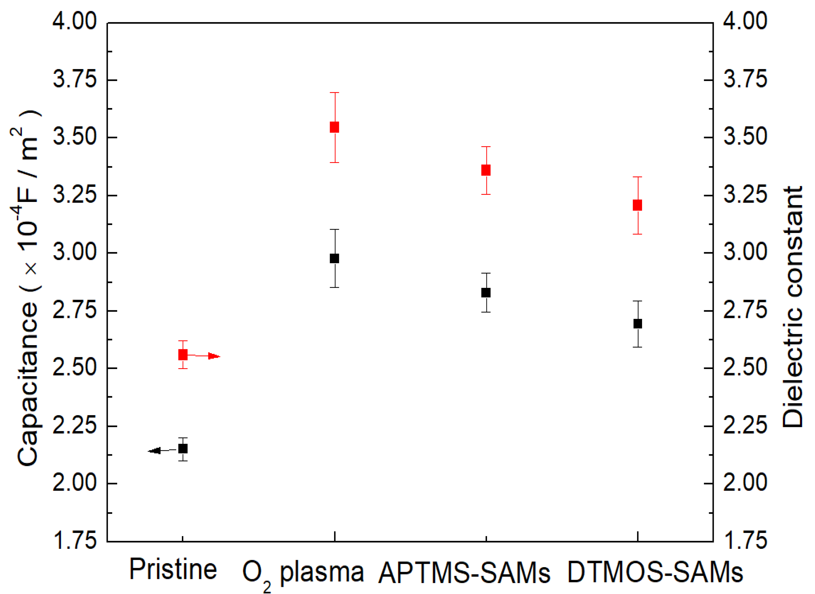
C-V curves of the fabricated MIS capacitors were measured. A typical MIS C-V feature: accumulation, transition, and depletion capacitances in order from negative to positive voltage, was observed for all samples (not shown). According to the measured accumulation capacitance (C) and the equation of k = Cd0A, the dielectric constant (k) of a dielectric film can be determined. Here, ε0 is absolute capacitivity in vacuum (8.85 × 10⁻¹² F/m), d is film thickness, and A is the area of the capacitor. Figure 2 compares the measured accumulation capacitance and the extracted k value for the pristine O2 plasma-irradiated, APTMS-SAMs, and DTMOS-SAMs p-SiOCH films. The k value of the pristine p-SiOCH film was 2.56 ± 0.06. After O2 plasma irradiation, the accumulation capacitance increased, thus increasing the k values to 3.54 ± 0.15. Following APTMS or DTMOS vapor treatment decreased the accumulation capacitance, thereby leading the k values to 3.20 ± 0.12 and 3.36 ± 0.10 for APTMS and DTMOS vapor treatment. Upon treatment, APTMS and DTMOS molecules react with the surface hydroxyl groups to form SAMs. The removal of Si-OH groups is responsible for the reduction of k values. Additionally, the k values of both samples with APTMS and DTMOS vapor treatments were larger than that of the pristine p-SiOCH film, attributing to the fact that APTMS or DTMOS molecules occupy the pores in the p-SiOCH film. APTMS molecules had a deeper diffusion depth into the p-SiOCH film due to their smaller size than DTMOS molecules, thereby stuffing more pores in the p-SiOCH film. This leads to a larger k value in the APTMS vapor-treated sample since the air in the pore has the minimum k value.
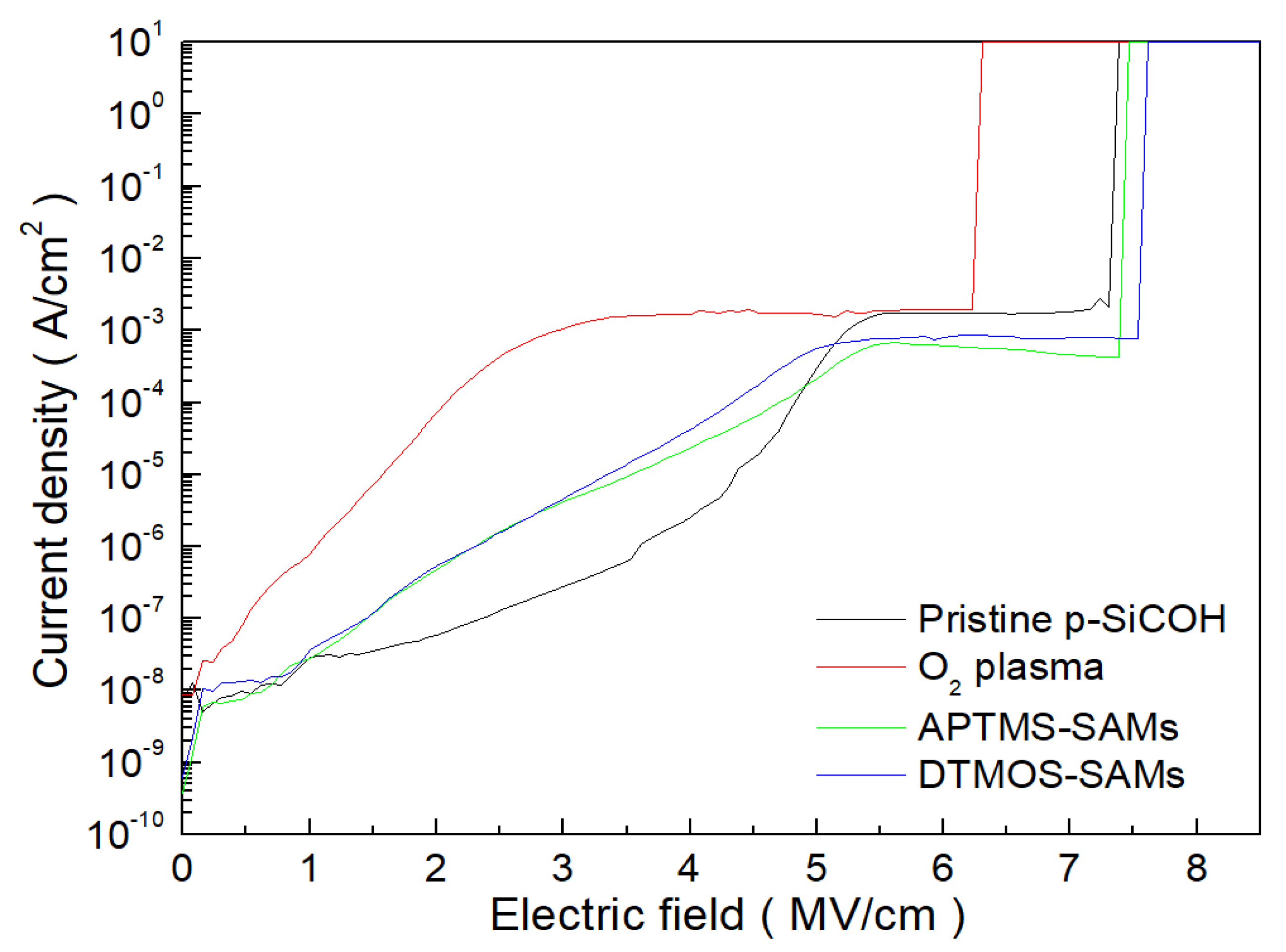
Figure 3 plots current density versus electric field (J-E) curves for the pristine, O2 plasma-irradiated, APTMS-SAMs, and DTMOS-SAMs p-SiOCH films from the I-V measurements. The applied voltage was transformed to the electric field (E) by dividing by the film’s thickness. The measured leakage current was transformed to the current density (J) by dividing it by the area of the electrode. For the pristine p-SiOCH film, the leakage current gradually increased with increasing the electric field, reached saturation, and jumped at least 3 orders of magnitude. The electric field at this jump for the pristine p-SiOCH film was 7.33 MA/cm, which is defined as the breakdown field. After O2 plasma irradiation, the current increased by 2~3 orders of magnitude and the breakdown field decreased by ~0.9 MV/cm, revealing that O2 plasma irradiation destroys the insulation properties of the p-SiOCH film. O2 plasma irradiation induces the formation of Si dangling bonds and polar silanol groups within the p-SiOCH film [6], thus increasing the conduction of leakage current. APTMS or DTMOS vapor treatment improved the electrical properties of the p-SiOCH film; the leakage current was reduced to the same level as the pristine p-SiOCH film and the breakdown field was increased, indicating that APTMS or DTMOS vapor treatment repairs damage induced by O2 plasma (i.e., the removal of Si dangling bonds and polar silanol groups). Additionally, this vapor treatment by organosilane molecules form SAM, providing another resistance against breakdown.
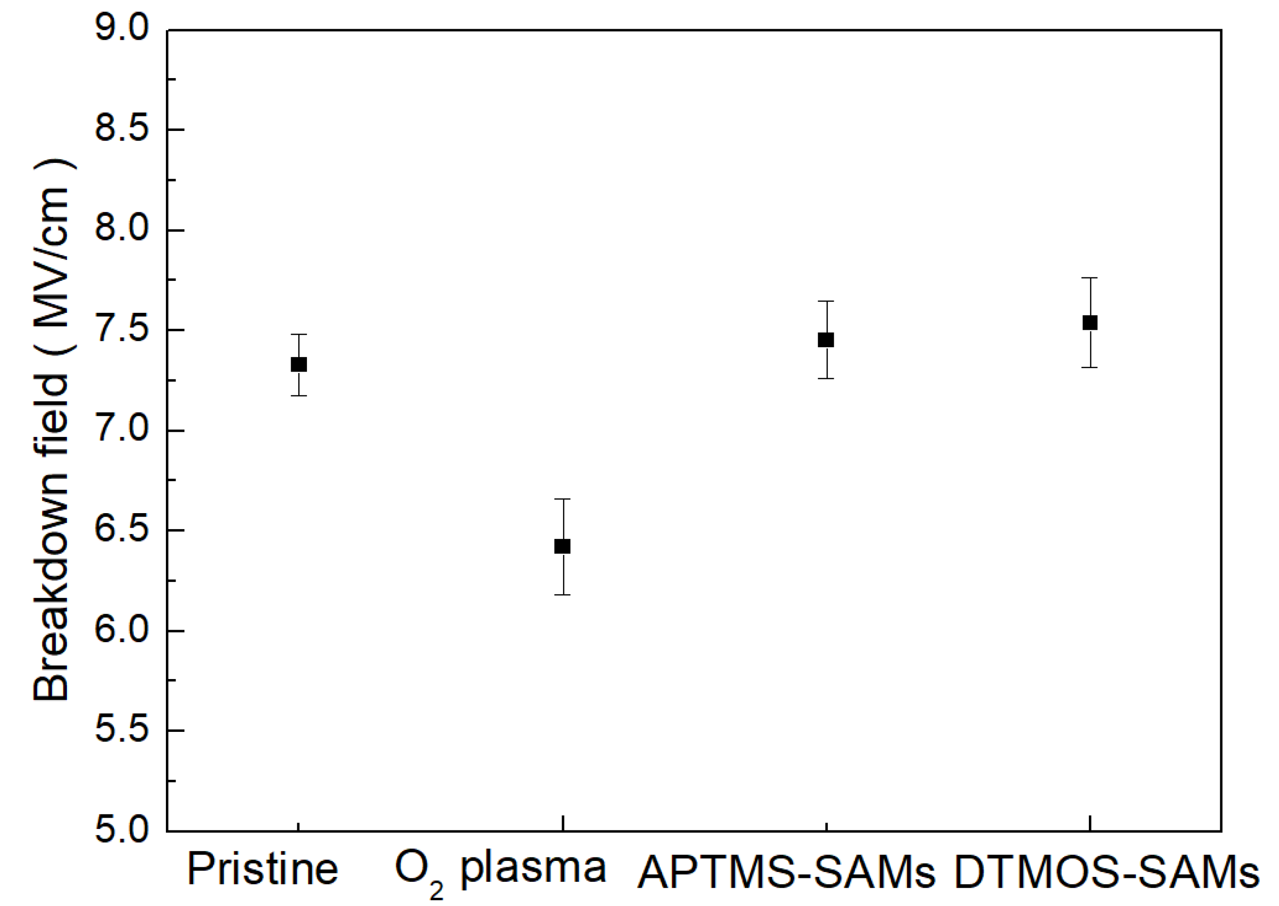
I-V measurements were conducted for each sample of the ten capacitors. Figure 4 compares the statistical breakdown fields for the pristine, O2 plasma-irradiated, APTMS-SAMs, and DTMOS-SAMs p-SiOCH films. For the pristine p-SiOCH film, the breakdown field was 7.33 ± 0.18 MV/cm. After O2 plasma irradiation, the breakdown field reduced to 6.43 ± 0.24 MV/cm due to plasma-induced damage on the film. Subsequent APTMS or DTMOS vapor treatment raised the breakdown field. The breakdown fields of APTMS-SAMs and DTMOS-SAMs samples were slightly larger than that of the pristine p-SiOCH film. The improvement is attributed to the removal of Si dangling bonds and polar silanol groups, the formation of SAMs, and the pore-stuffing effect of APTMS or DTMOS vapor treatment [24,25]. Additionally, DTMOS vapor treatment exhibited a larger increase in the breakdown field than APTMS vapor treatment, suggesting that the chain length of the SAMs precursor plays an important part in the improvement of the breakdown field.
The long-term reliability of the SAMs-formed p-SiOCH films by using APTMS or DTMOS molecules in the vapor phase was assessed by TDDB tests. In TDDB tests, three fields were applied, and ten samples were measured for each condition of the dielectric time to failure (TTF).
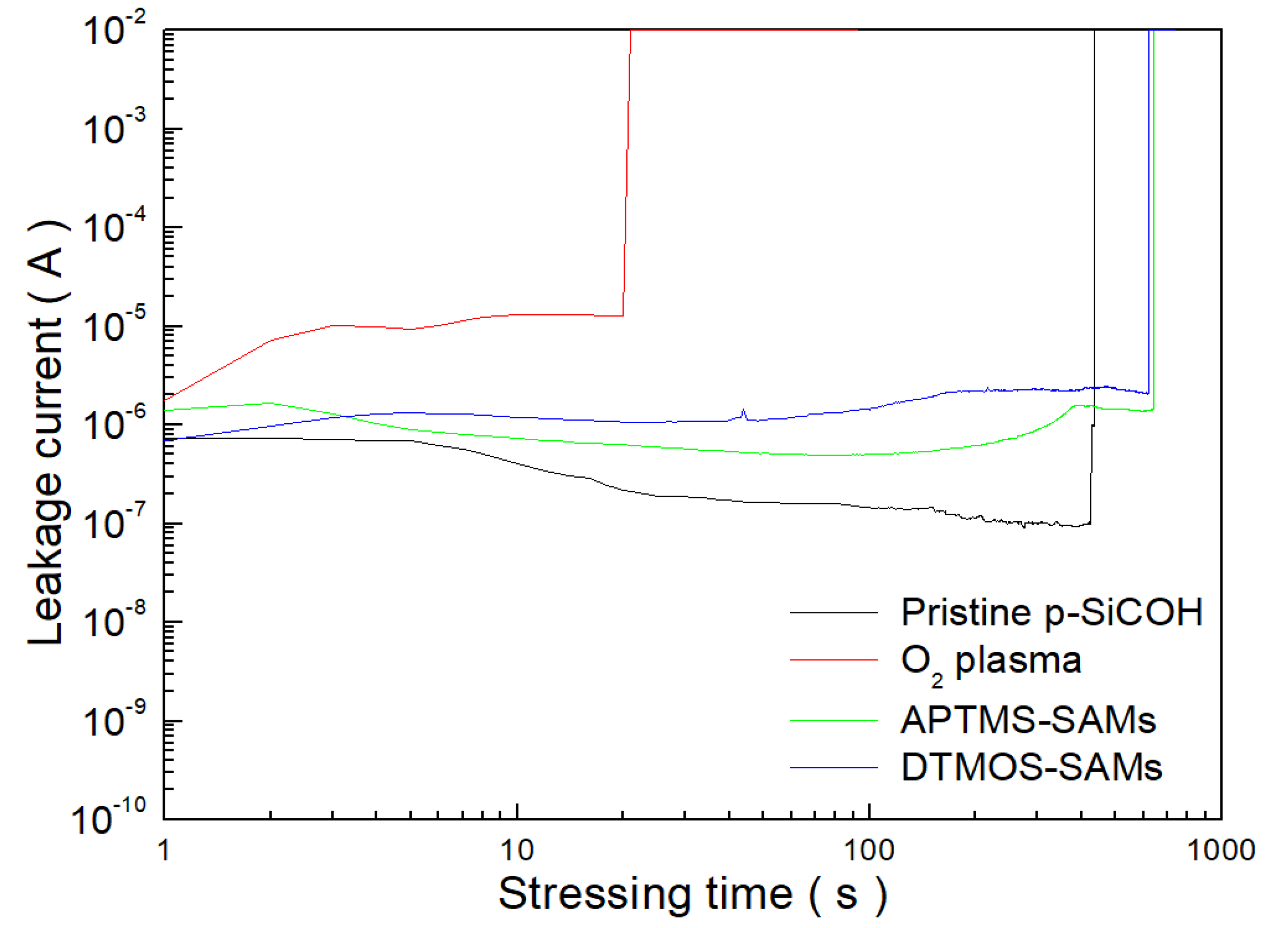
Figure 5 shows the degradation and breakdown characteristics of the pristine, O2 plasma-irradiated APTMS-SAMs and DTMOS-SAMs p-SiOCH films during the electrical stress. For the pristine p-SiOCH film, the leakage current gradually decreased in the initial state and remained constant before breakdown. The decrease in the leakage current at the beginning of the stressing time is believed to be caused by electron trapping [26]. After O2 plasma irradiation, the leakage current increased first as the stressing time increased and then saturated until the breakdown. O2 plasma-induced defects led to the increased leakage current and TDDB degradation. The APTMS-SAMs and DTMOS-SAMs samples displayed different features in the time-dependent leakage current. The leakage current gradually decreased for APTMS-SAMs and increased for DTMOS-SAMs. For DTMOS-SAMs samples, the increasing magnitude was lower than that of O2 plasma-irradiated samples, indicating that O2 plasma-induced defects are repaired by SAMs processing.
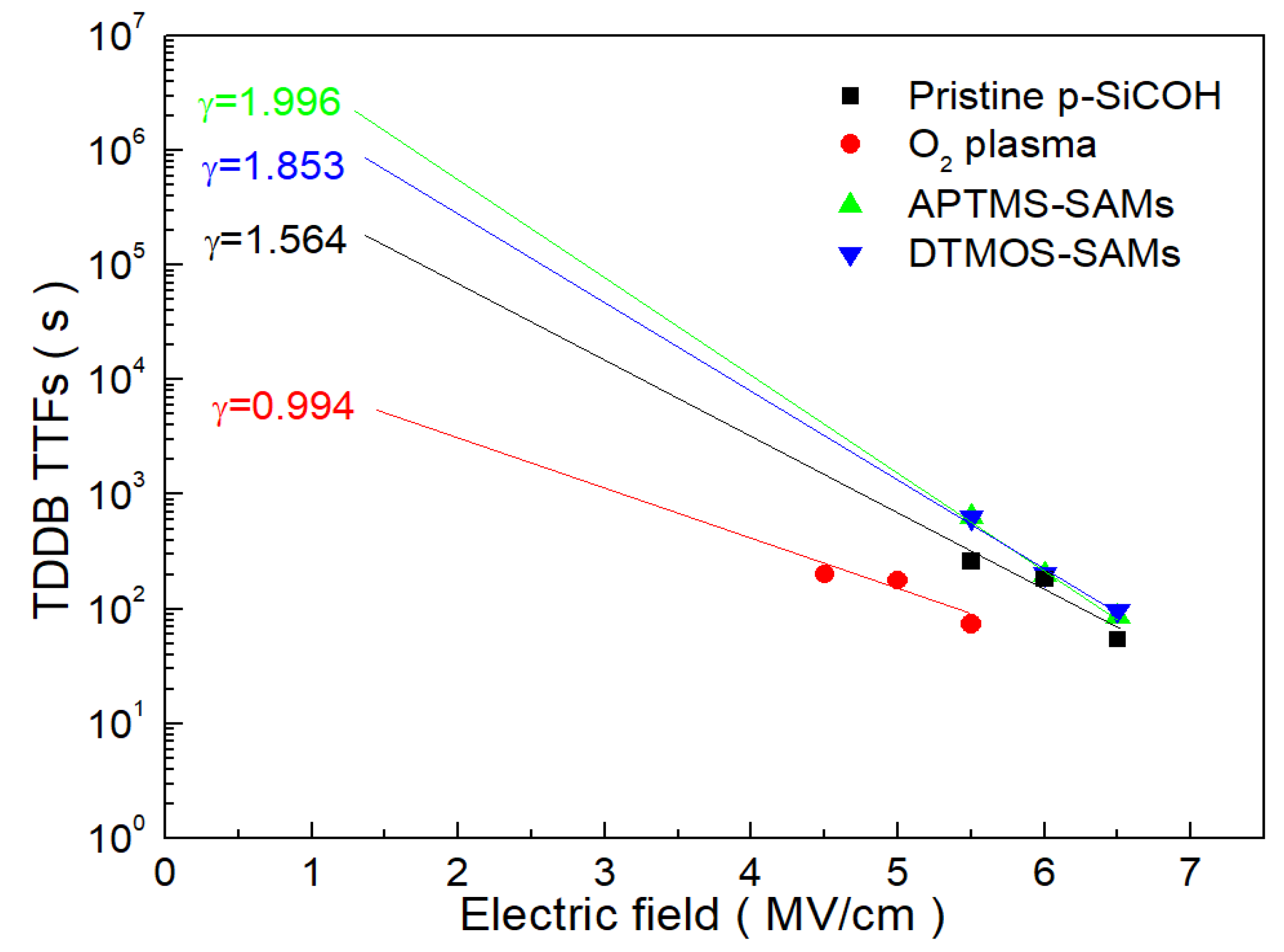
Figure 6 compares TTFs as a function of the stressing field for the pristine, O2 plasma-irradiated APTMS-SAMs and DTMOS-SAMs p-SiOCH films. The TTFs decreased with increasing the applied field for all samples, indicating that the electric field controls the breakdown reliability of a dielectric film. Hence, the E model (TTF ∼exp(-γE)) was used to evaluate the effect of the electric field on the dielectric breakdown time in this study [26,27]. Here, γ is a field acceleration factor; a larger γ value represents a stronger electric-field dependence for TDDB TTFs and has a longer dielectric failure time in a low-operation field. Figure 7 also lists the extracted γ values for p-SiOCH films with various conditions. For p-SiOCH films subjected to O2 plasma irradiation, the TTFs degraded and the degradation magnitude was amplified with decreasing the stressing field. The γ value also reduced to 0.994 from 1.564. Under O2 plasma irradiation, the generated VUV photon, charged particle, and oxygen radicals damage the p-SiOCH film, leading to the degradation of TDDB reliability [28]. Subsequent APTMS or DTMOS vapor treatment on the O2 plasma-irradiated p-SiOCH film promoted TTFs and increased γ value. These TDDB reliability characteristics were larger than those of the pristine p-SiOCH film. As a result, APTMS or DTMOS vapor treatment can repair O2 plasma-induced damage on the p-SiOCH film. Additionally, SAMs are formed at the film’s surface, and pores within the film are sealed and stuffed, thereby leading to TDDB improvement. Comparing TDDB TTFs between APTMS-SAMs and DTMOS-SAMs samples, a crossover in the plot of TDDB TTFs versus stressing field was observed. When stressed at a higher field (6.5 MV/cm), the DTMOS-SAMs sample had a larger TTF, similar to the result of the breakdown field. As the stressing field decreased to 6.0 MV/cm, instead, the APTMS-SAMs sample had larger TTFs; the characteristics yielded the larger γ value for the APTMS-SAMs sample.
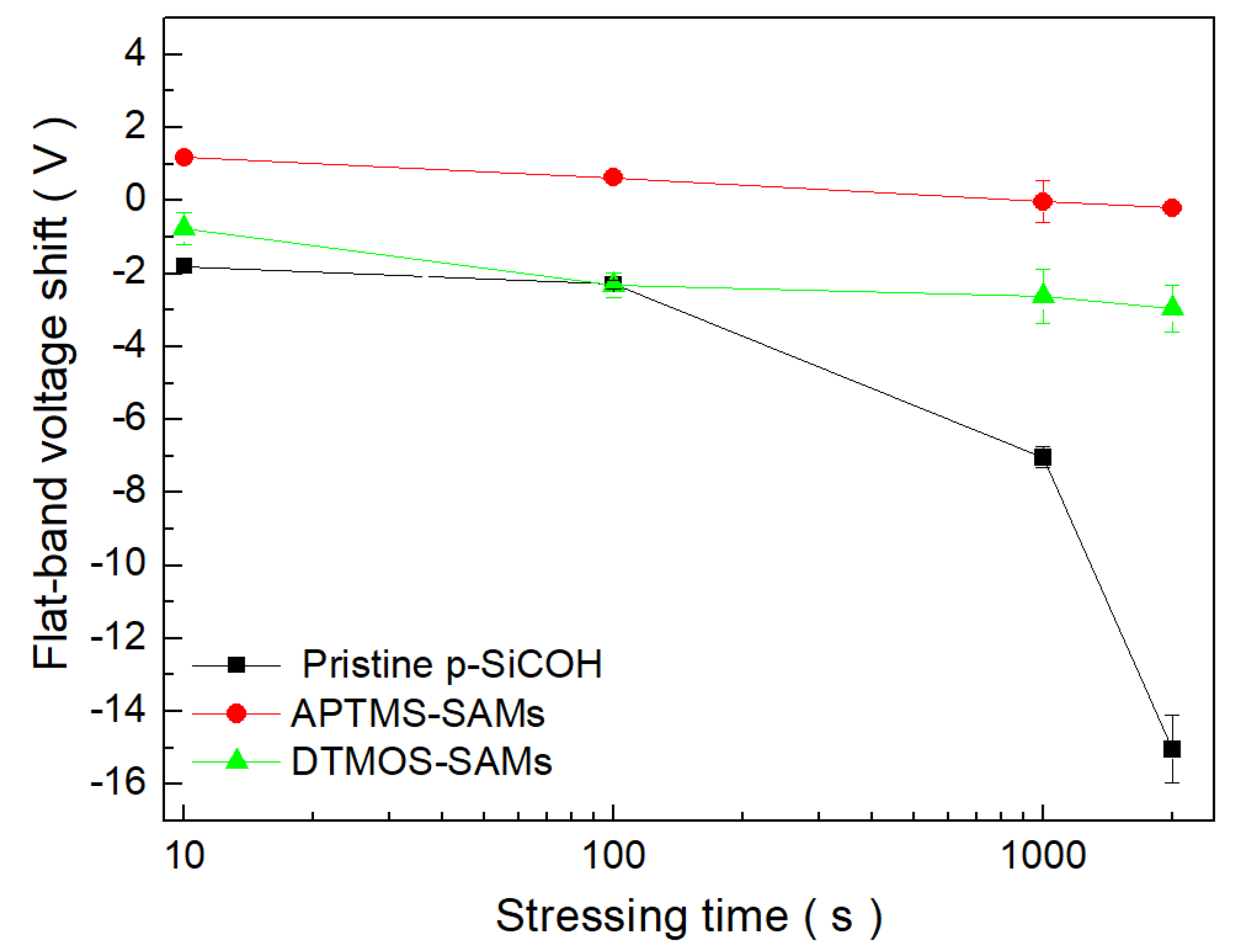
The electrical stress at positive polarity was conducted to evaluate the barrier capacity of the formation SAMs between Cu and p-SiOCH films. Under positive-polarity electrical stress, metal ions are formed and drift into the dielectric with the assistance of the external electric field [25]. In this study, the samples were stressed under a positive-polarity electrical field at various fields. Then, C-V and I-V measurements were made. From the measured C-V curves, the shift of the flatband voltage (Vfb) can be determined, which can be an indicator of the amount of drifted metal ions. Figure 8 plots Vfb shifts under electrical stress at 5 MV/cm with varying stressing-time for the pristine, APTMS-SAMs, and DTMOS-SAMs p-SiOCH films. The data presented here were collected from five measurements. For the pristine p-SiOCH film after positively-biased electric stress, Vfb shifted to the negative-voltage direction and the shifting magnitude increased with stressing time, indicating that positively-charged ions (i.e., Cu ions) are trapped introduced into the film and the amount increased with stressing time [12]. As SAMs formed on the p-SiOCH film either derived from APTMS or DTMOS vapor treatment, the Vfb shifting magnitude became smaller compared to the pristine sample, revealing that both SAMs derived from APTMS and DTMOS vapor treatment can block the drift of Cu ions. For APTMS-SAMs samples, no negative shift in Vfb was detected, but it showed a positive shift. This indicates that Cu ions do not diffuse into the p-SiOCH film, but negative charges are generated and introduced into the film. It can be concluded that SAMs formed by APTMS vapor treatment is a superior barrier for Cu/porous low-k integration scheme.
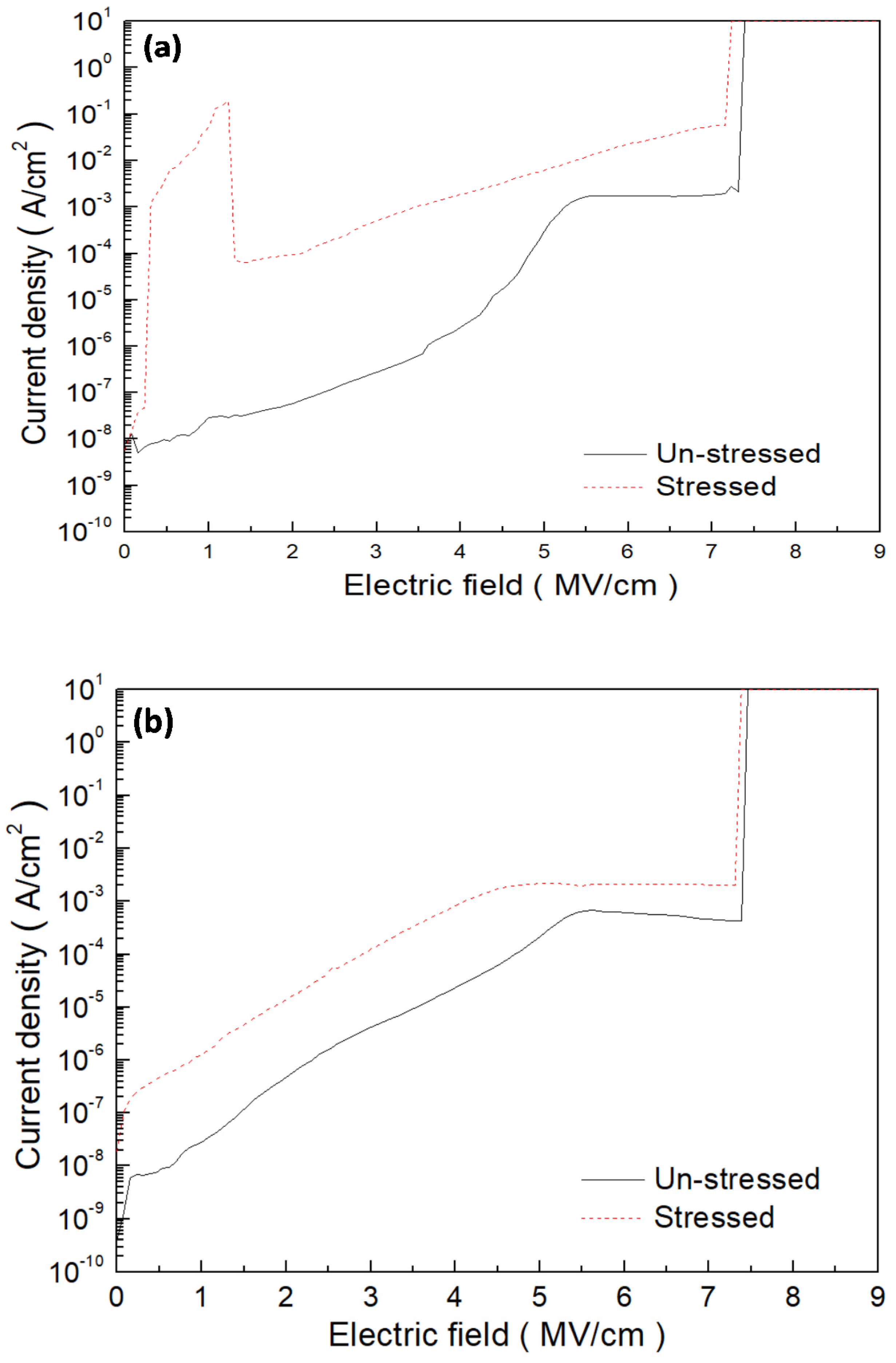
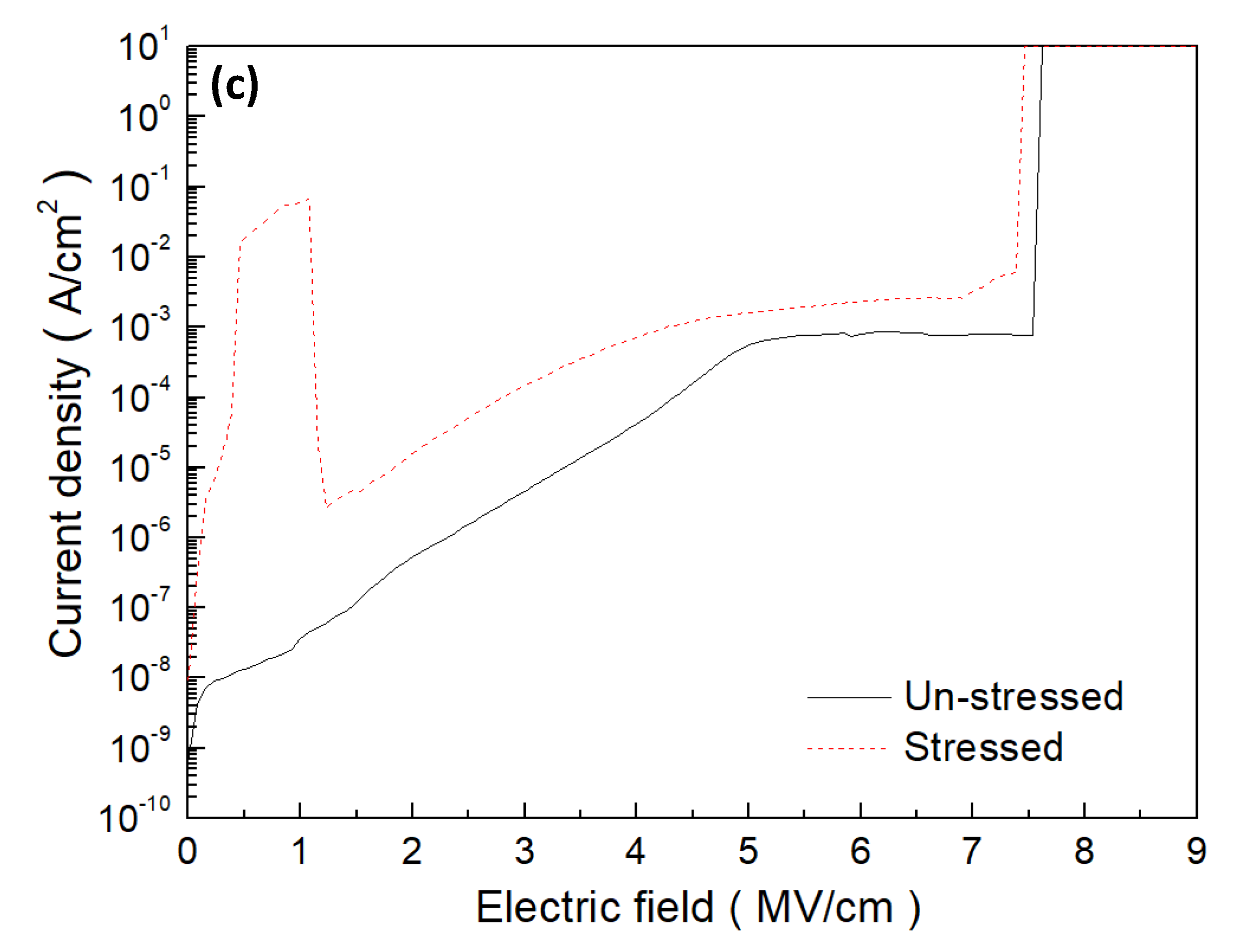
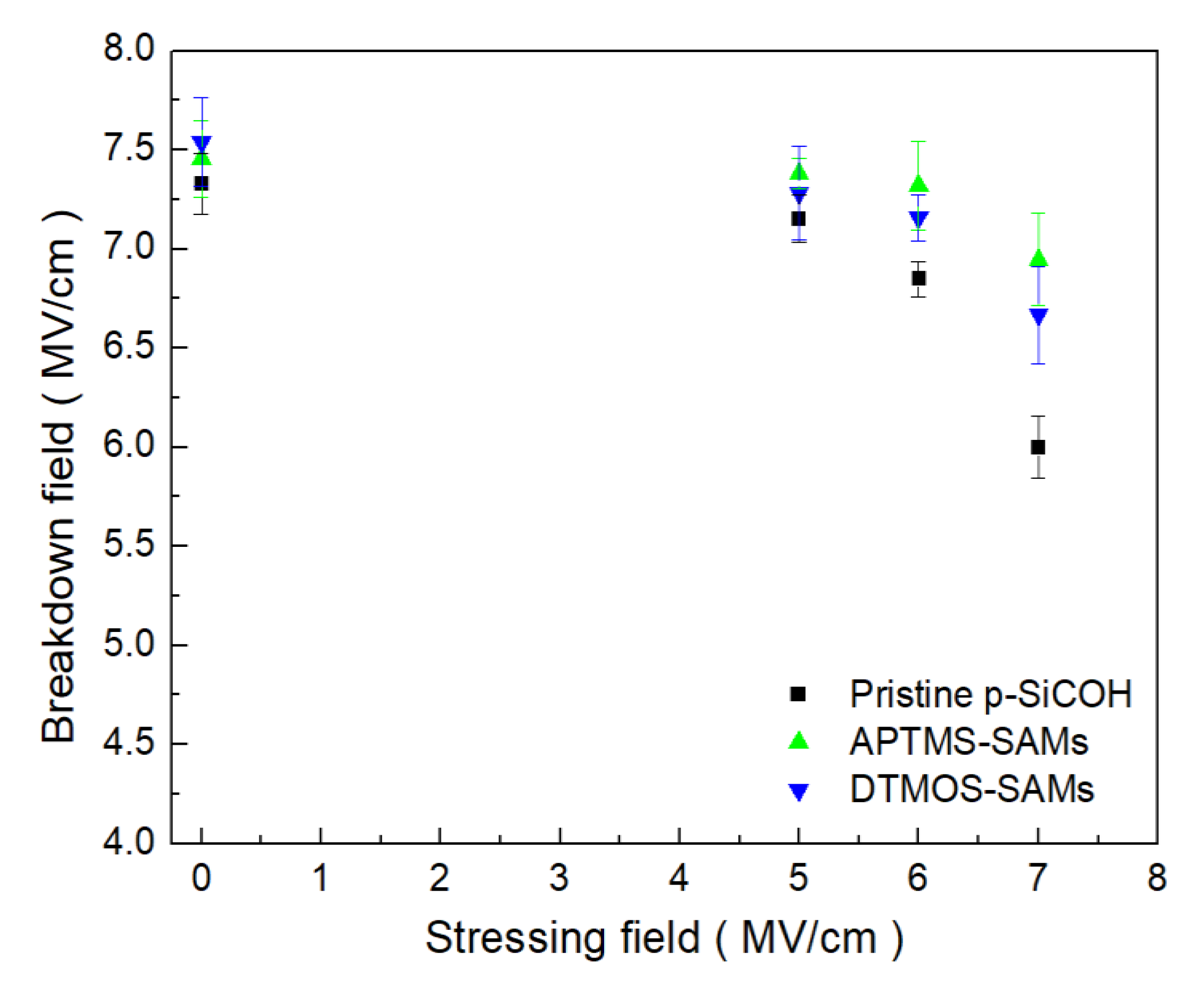
The samples were also applied to electric stress with varying fields for 1000 s and then I-V measurements the samples were conducted. Figure 8a–c plot the comparison of I-V curves before and after electrical stress at 5 MV/cm for the pristine, APTMS-SAMs, and DTMOS-SAMs p-SiOCH films, respectively. For all stressed samples, the leakage current increased and the breakdown field reduced as compared to the fresh samples. In the pristine and DTMOS-SAMs p-SiOCH films after electric stress, a peak (or hump) appeared in the low-voltage range. Under electrical stress, a positive bias is applied to the metal gate of MIS capacitors, allowing mobile ions to drift into the p-SiOCH film. As electrical stress provides enough time for ample metal ions to drift, the subsequent I-V measurement with negative voltage sweep allows mobile charges to drift back to the previously established metal-dielectric interface in the external electric field, thereby contributing to conduction. Therefore, the appearing peak in the I-V curve is associated with the drift of Cu ions [26]. On the other hand, this peak was not observed for APTMS-SAMs samples after electrical stress at 5 MV/cm, indicating that APTMS-SAMs provide a superior barrier capacitor as compared to DTMOS-SAMs. Figure 9 compares the reduction of the breakdown field as a function of the stressing field for the pristine, APTMS-SAMs, and DTMOS-SAMs p-SiOCH films. As the stressing fields increased, the reduction of the breakdown field was amplified for all samples. For the pristine p-SiOCH films, the reduction magnitude with the stressing field became more pronounced, indicating that more Cu ions drift into the film under electrical stress at higher fields. APTMS-SAMs and DTMOS-SAMs samples had a relatively small reduction in the breakdown field, revealing that the formation SAMs has an effective barrier against Cu migration. Similar to other results in this study, APTMS-SAMs samples had the lowest reduction in the breakdown field after being subjected to electrical stress, elucidating that the formation SAMs derived from APTMS has the best blocking ability.
To evaluate the adhesion promotion of the formation SAMs for Cu/p-SiOCH samples, stud-pull tape tests were conducted to measure the adhesion ability. Eighty square dots were tested for each sample. Table 3 lists the tape test results. For the as-deposited Cu/p-SiOCH sample without the insertion of SAMs, 72.5% of samples were delaminated, indicating poor adhesion between the porous low-k film and Cu. As SAMs were inserted between p-SiOCH and Cu films, all 80 square dots remained intact after stud-pull tape for APTMS-SAMs and DTMOS-SAMs samples, representing that the adhesion of Cu/p-SiOCH is greatly improved by the formation of SAMs. Hence, SAMs derived from APTMS or DTMOS are suitable to act as an adhesive in Cu interconnects.

4. Conclusions

In this study, SAMs were formed on the p-SiOCH films by using APTMS or DTMOS molecules in the vapor phase. Effects of the formation SAMs on the electrical characteristics and reliability of p-SiOCH films were characterized and compared. SAMs were successfully formed at the surface of the p-SiOCH film by using APTMS or DTMOS vapor treatment. Both formation SAMs enhanced the breakdown field, TDDB TTFs, Cu barrier capacity, and adhesion with Cu. Additionally, APTMS-SAMs had a larger improvement than DTMOS-SAMs, revealing that APTMS-SAMs are a suitable candidate for Cu barrier and adhesive layers in the advanced Cu/p-SiOCH integration scheme.

Author Contributions

Conceptualization, methodology, writing—original draft preparation, writing—review and editing; Y.-L.C.; validation, formal analysis: J.K., H.-W.Z. and C.-Y.L., investigation: J.K., H.-W.Z. and C.-Y.L. All authors have read and agreed to the published version of the manuscript.

Funding

This research received no external funding.

Institutional Review Board Statement

Not applicable.

Informed Consent Statement

Not applicable.

Data Availability Statement

The authors confirm that the data supporting the findings of this study are available within the article.

Acknowledgments

The author would like to thank the National Science Council of the Republic of China, Taiwan, for financially supporting this research under Contract No. MOST-109-2221-E-260-010-MY2.

Conflicts of Interest

The authors declare no conflict of interest.

References

  1. Maex, K.; Baklanov, M.R.; Shamiryan, D.; Iacopi, F.; Brongersma, S.H.; Yanovitskaya, Z.S. Low dielectric constant materials for microelectronics. J. Appl. Phys. 2003, 93, 8793–8841. [Google Scholar] [CrossRef]
  2. Grill, A. Porous pSiCOH ultralow-k dielectrics for chip interconnects prepared by PECVD. Annu. Rev. Mater. Res. 2009, 39, 49–69. [Google Scholar] [CrossRef]
  3. Grill, A.; Gates, S.M.; Ryan, T.E.; Nguyen, S.V.; Priyadarshini, D. Progress in the development and understanding of advanced low k and ultralow k dielectrics for very large-scale integrated interconnects—State of the art. Appl. Phys. Rev. 2014, 1, 011306. [Google Scholar] [CrossRef] [Green Version]
  4. Grill, A. Plasma enhanced chemical vapor deposited SiCOH dielectrics: From low-k to extreme low-k interconnect materials. J. Appl. Phys. 2003, 93, 1785. [Google Scholar] [CrossRef]
  5. Cheng, Y.L.; Lin, B.H.; Huang, S.W. Effect of O2 Plasma Treatment on Physical, Electrical, and Reliability Characteristics of Low Dielectric Constant Materials. Thin Solid Films 2014, 572, 44–50. [Google Scholar] [CrossRef]
  6. Baklanov, M.R.; de Marneffe, J.-F.; Shamiryan, D.; Urbanowicz, A.M.; Shi, H.; Rakhimova, T.V.; Huang, H.; Ho, P.S. Plasma processing of low-k dielectrics. J. Appl. Phys. 2013, 113, 041101-1. [Google Scholar] [CrossRef]
  7. Shi, H.; Huang, H.; Bao, J.; Liu, J.; Ho, P.S. Roles of ions, photons, and radicals in inducing plasma damage to ultra low-k dielectrics. J. Vac. Sci. Technol. B 2012, 30, 011206-1. [Google Scholar] [CrossRef]
  8. Hosseini, M.; Koike, J. Amorphous CoTix as a liner/diffusion barrier material for advanced copper metallization. J. Alloys Compd. 2017, 721, 134–142. [Google Scholar] [CrossRef]
  9. Fang, K.L.; Tsui, B.Y. Metal drift induced electrical instability of porous low dielectric constant film. J. Appl. Phys. 2003, 93, 5546. [Google Scholar] [CrossRef] [Green Version]
  10. Chen, F.; Bravo, O.; Harmon, D.; Shinosky, M.; Aitken, J. Cu/low-k dielectric TDDB reliability issues for advanced CMOS technologies. Microelectron. Reliab. 2008, 48, 1375–1383. [Google Scholar] [CrossRef]
  11. Li, Z.; Tian, Y.; Teng, C.; Cao, H. Recent Advances in Barrier Layer of Cu Interconnects. Materials 2020, 48, 5049. [Google Scholar] [CrossRef] [PubMed]
  12. Hosseini, M.; Ando, D.; Sutou, Y.; Koike, J. Co and CoTix for contact plug and barrier layer in integrated circuits. Microelectron. Eng. 2018, 189, 78. [Google Scholar] [CrossRef]
  13. Caro, A.M.; Maes, G.; Borghs, G.; Whelan, C.M. Screening self-assembled monolayers as Cu diffusion barriers. Microelectron. Eng. 2008, 85, 2047–2050. [Google Scholar] [CrossRef]
  14. Brady-Boyd, A.; O’Connor, R.; Armini, S.; Selvaraju, V.; Hughes, G.; Bogan, J. On the use of (3-trimethoxysilylpropyl)diethylenetriamine self-assembled monolayers as seed layers for the growth of Mn based copper diffusion barrier layers. Appl. Surf. Sci. 2018, 427, 260–266. [Google Scholar] [CrossRef]
  15. Aldakov, D.; Bonnassieux, Y.; Geffroy, B.; Palacin, S. Selective electroless copper deposition on self-assembled dithiol monolayers. ACS Appl. Mater. Interfaces 2009, 1, 584–589. [Google Scholar] [CrossRef] [PubMed]
  16. Uedono, A.; Armini, S.; Zhang, Y.; Kakizaki, T.; Krause-Rehberg, R.; Anwand, W.; Wagner, A. Surface sealing using self-assembled monolayers and its effect on metal diffusion in porous low-K dielectrics studied using monoenergetic positron beams. Appl. Surf. Sci. 2016, 368, 272–276. [Google Scholar] [CrossRef]
  17. Sharma, S.; Kumar, M.; Rani, S.; Kumar, D. Deposition and characterization of 3-aminopropyltrimethoxysilane monolayer diffusion barrier for copper metallization. Metall. Mater. Trans. B 2014, 46, 928–932. [Google Scholar] [CrossRef]
  18. Ganesan, P.G.; Singh, A.P.; Ramanath, G. Diffusion barrier properties of carboxyland amine-terminated molecular nanolayers. Appl. Phys. Lett. 2004, 85, 579. [Google Scholar]
  19. Cheng, Y.L.; Lee, C.Y.; Peng, W.F.; Chen, G.S.; Fang, J.S. Comparison of Self-Assembled Monolayers on SiO2 and Porous SiOCH, Dielectrics by Decyltrimethoxysilane Vapor Treatment. Coatings 2022, 12, 926. [Google Scholar] [CrossRef]
  20. Cheng, Y.L.; Lee, C.Y.; Huang, J.W.; Chen, G.S.; Fang, J.S. Comparison of Various Low Dielectric Constant Materials. Thin Solid Films 2018, 660, 871–878. [Google Scholar]
  21. Cheng, Y.L.; Leon, K.W.; Huang, J.F.; Chang, W.Y.; Chang, Y.M.; Leu, J. Effect of moisture on electrical properties and reliability of low dielectric constant materials. Microelectron. Eng. 2014, 114, 12–16. [Google Scholar] [CrossRef]
  22. Vanstreels, K.; Ciofi, I.; Barbarin, Y.; Baklanov, M. Influence of porosity on dielectric breakdown of ultralow-k dielectrics. J. Vac. Sci. Technol. B 2013, 31, 050604. [Google Scholar] [CrossRef]
  23. Kao, K.C.; Chang, W.Y.; Chang, Y.M.; Leu, J.; Cheng, Y.L. Comprehensively Study of UV Curing Time Effect on Physical, Electrical, and Reliability Properties for Low Dielectric Constant Materials. J. Vac. Sci. Technol. A 2014, 32, 061514. [Google Scholar] [CrossRef] [Green Version]
  24. Armini, S.; Prado, J.L.; Krishtab, M.; Swerts, J.; Verdonck, P.; Meersschaut, J.; Conard, T.; Blauw, M.; Struyf, H.; Baklanov, M.R. Pore sealing of k 2.0 dielectrics assisted by self-assembled monolayers deposited from vapor phase. Microelectron. Eng. 2014, 120, 240–245. [Google Scholar] [CrossRef]
  25. Ishikawa, D.; Kobayashi, A.; Nakano, A.; Kimura, Y.; Matsushita, K.; Kobayashi, N.; Ditmer, G.; Kiermasz, A. Plasma-enhanced atomic layer deposition sealing property on extreme low-k film with k = 2.0 quantified by mass metrology. Jpn. J. Appl. Phys. 2013, 52, 05FG01. [Google Scholar] [CrossRef]
  26. He, M.; Lu, T.-M. Metal-Dielectric Interfaces in Gigascale Electronics: Thermal and Electrical Stability; Series in Materials Science; Springer: Berlin/Heidelberg, Germany, 2012; Volume 157. [Google Scholar]
  27. Mcpherson, J.W. Time dependent dielectric breakdown physics—Models revisited. Microelectron. Reliab. 2012, 52, 1753–1760. [Google Scholar] [CrossRef]
  28. Chen, F.; Shinosky, M.A. Electron fluence driven, Cu catalyzed, interface breakdown mechanism for BEOL low-k time dependent dielectric breakdown. Microelectron. Reliab. 2014, 54, 529–540. [Google Scholar] [CrossRef]
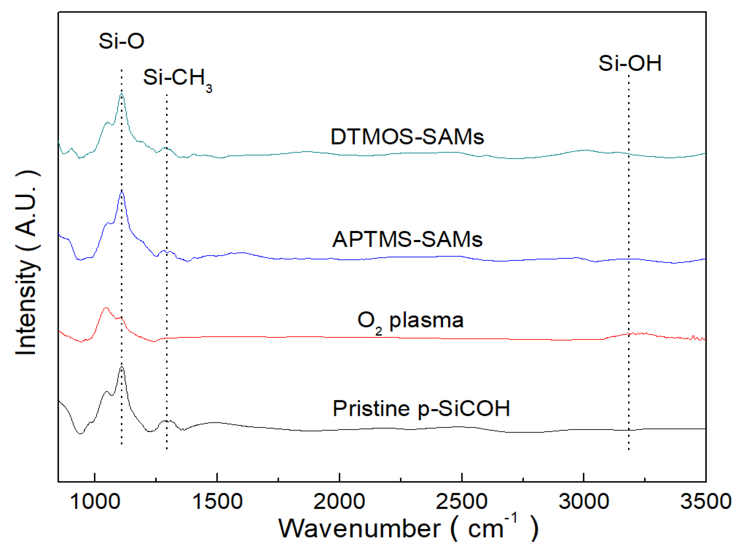
Figure 1. FT-IR spectra of pristine, O2 plasma-irradiated, APTMS-SAMs, and DTMOS-SAMs p-SiOCH films.
Coatings 13 00507 g001
Figure 2. Comparison of accumulation capacitance and dielectric constant of pristine, O2 plasma-irradiated, APTMS-SAMs, and DTMOS-SAMs p-SiOCH films.
Coatings 13 00507 g002
Figure 3. J-E curves of pristine, O2 plasma-irradiated, APTMS-SAMs, and DTMOS-SAMs p-SiOCH films.
Coatings 13 00507 g003
Figure 4. Comparison of breakdown fields of pristine, O2 plasma-irradiated, APTMS-SAMs, and DTMOS-SAMs p-SiOCH films.
Coatings 13 00507 g004
Figure 5. Plots of leakage current versus the stress time (I-t) for pristine, O2 plasma-irradiated, APTMS-SAMs, and DTMOS-SAMs p-SiOCH films under TDDB tests.
Coatings 13 00507 g005
Figure 6. TDDB TTFs of pristine, O2 plasma-irradiated, APTMS-SAMs, and DTMOS-SAMs p-SiOCH films as a function of the stressing electric field.
Coatings 13 00507 g006
Figure 7. Flatband voltage shifts of pristine, APTMS-SAMs and DTMOS-SAMs p-SiOCH films after electric stress at 5 MV/cm with varying intervals.
Coatings 13 00507 g007
Figure 8. Comparison of I-E curves after being subjected to electric stress at 5 MV/cm: (a) pristine; (b) APTMS-SAMs; (c) DTMOS-SAMs p-SiOCH films.
Coatings 13 00507 g008aCoatings 13 00507 g008b
Figure 9. Reduction of breakdown field after electric stress at various fields for pristine, APTMS-SAMs, and DTMOS-SAMs p-SiOCH films.
Coatings 13 00507 g009
Table 1. Chemical formula and properties of APTMS and DTMOS molecules.
SAMs PrecursorMolecular FormularStructureMolar Mass (g/mole)Density (g/cm3)Boiling Point at 760 mmHg (°C)Projected Length (nm)
Head GroupChainFunctional Group
APTMSNH2(CH2)3Si(OCH3)3-Si(OCH3)3(CH2)3-NH2179.291.021941.45
DTMOSCH3((CH2)9)Si(OCH3)3-Si(OCH3)3(CH2)9-CH3262.4610.9213.62.25
Table 2. Properties of the formation SAMs derived from APTMS and DTMOS molecules.
SAMsThickness (nm)Contact Angle (Degree)Roughness (RMS; nm)
APTMS-SAMs1.52 ± 0.1973.20.314
DTMOS-SAMs3.72 ± 0.1882.60.351
Table 3. Results of stud-pull tape tests for the pristine, APTMS-SAMs, and DTMOS-SAMs p-SiOCH films.
StructureStud-Pull Tape Result
Cu/p-SiOCH/Si58/80 (72.5%)
Cu/APTMS-SAMs/p-SiOCH/Si0/80 (0%)
Cu/DTMOS-SAMs/p-SiOCH/Si0/80 (0%)
Note: Failure/Test samples (Failure rate).
Disclaimer/Publisher’s Note: The statements, opinions and data contained in all publications are solely those of the individual author(s) and contributor(s) and not of MDPI and/or the editor(s). MDPI and/or the editor(s) disclaim responsibility for any injury to people or property resulting from any ideas, methods, instructions or products referred to in the content.