Abstract
In this study, we fabricate a counter electrode by coating a Pt ribbon onto a fluorine-doped tin oxide glass substrate with a Pt layer. The Pt ribbon gives rise to a protrusive structure of the counter electrode, produced by photolithography, sputtering and lift-off processes. The experimental results reveal that the photoelectric efficiency of the dye-sensitized solar cell (DSSC) with the Pt ribbon (5.32%) is 21% higher than that of the DSSC without a Pt ribbon (4.38%). This infers that Pt ribbons can increase the photoelectric efficiencies of DSSCs. The DSSC with the Pt ribbon has a large photoelectric efficiency of 5.32%, not only because the protrusive structure has specific channels for directional electron transport, but also because of its large surface area. The method that is proposed herein has the advantages of a low production cost and easy fabrication that can be applied to various electrode structures.
1. Introduction
Solar cells are photovoltaic devices because they can convert solar energy into electricity [1,2,3,4,5,6]. Dye-sensitized solar cells (DSSCs) have attracted much attention in recent years owing to their appealing manufacturing costs, simple design and high flexibility.
A review paper has reported that the preparation methods of the counter electrodes in DSSCs include electrochemical deposition, chemical vapor deposition, thermal decomposition, hydrothermal reaction, polymerization, chemical reduction and sputtering deposition [7]. All of these methods aim to obtain counter electrodes with high conductivity, high catalytic activity, good stability and low costs. Each of the preparation methods has its own advantages and disadvantages. There is no omnipotent method for depositing counter electrodes, and the preparation methods are chosen on the basis of the specific situation [7].
Counter electrodes such as Pt metal, carbon materials, conductive polymers and hybrid materials play important roles in determining the energy conversion efficiencies and manufacturing costs of DSSCs. A counter electrode must possess a large conductivity, high catalytic activity, good stability and low cost. Pt metal meets the first three requirements for counter electrodes and is the most frequently used material in counter electrodes [7]. Carbon materials, conductive polymers and hybrid materials satisfy one or two of the four requirements [7]. Pt is expensive compared to other counter electrodes. However, Fang et al. reported that the thicknesses of Pt layers exerts an insignificant effect on the photovoltaic efficiencies of DSSCs [8]. Therefore, the fabrication costs of DSSCs with Pt counter electrodes can be decreased by using a small amount of Pt. Therefore, Pt metal is studied in this work.
A conventional counter electrode is made of a layer that comprises Pt nanoparticles. Pt nanoparticles facilitate the reduction of oxidized electrolyte molecules owing to their large surface area, good electrocatalytic activity and large conductivity. Fang et al. studied the effect of the thickness of the Pt layer on the energy conversion efficiency of a DSSC [8]. Their experimental results revealed that the photoelectric efficiency of the DSSC increases from 0.38% to 4.92% as the thickness of the Pt layer increases from 0 nm to 10 nm, since the large grain size of the Pt nanoparticles in a thick layer promotes the reduction of the oxidized electrolyte. However, the photoelectric efficiency of the DSSC exhibited no significant change as the thickness of the Pt layer increased from 10 nm to 415 nm. As a result, a thin Pt layer is enough to induce a large photoelectric efficiency in a DSSC. Özkan et al. studied the effect of the inkjet printing and drop casting of Pt layers on the photoelectric efficiencies of DSSCs [9]. The efficiency (7.6%) of the DSSC fabricated by inkjet printing exceeds that (6.5%) of the DSSC fabricated by drop casting because the Pt nanoparticles have a larger grain size in inkjet printing than in drop casting. This result reveals that inkjet printing can significantly increase the efficiencies of DSSCs. Venkatesan et al. investigated the effect of a Pt layer deposited with poly(3,4-ethylene dioxythiophene) (PEDOT) on the photoelectric efficiency of a DSSC [10]. Their experimental results revealed that the photoelectric efficiency (14.29%) of the DSSC involving the PEDOT-deposited Pt layer exceeded that (12.50%) of the DSSC with a plain Pt layer because the aggregation of the PEDOT molecules on the Pt nanoparticles increases the surface area of the counter electrode in the former. This result displays that the deposition of PEDOT on plain Pt layers enhances the efficiency of DSSCs. These three references reveal that a large surface area of the counter electrodes facilitates the reduction of oxidized electrolyte molecules, increasing the efficiency of DSSCs.
This study proposes a method for increasing the photoelectric efficiencies of DSSCs using Pt patterns via photolithography, sputtering and lift-off processes. In the same way, photolithography, sputtering and lift-off processes can also be used to deposit other materials for increasing the photoelectric efficiencies of DSSCs. Therefore, the method proposed herein can be used for different types of counter electrodes.
2. Materials and Methods
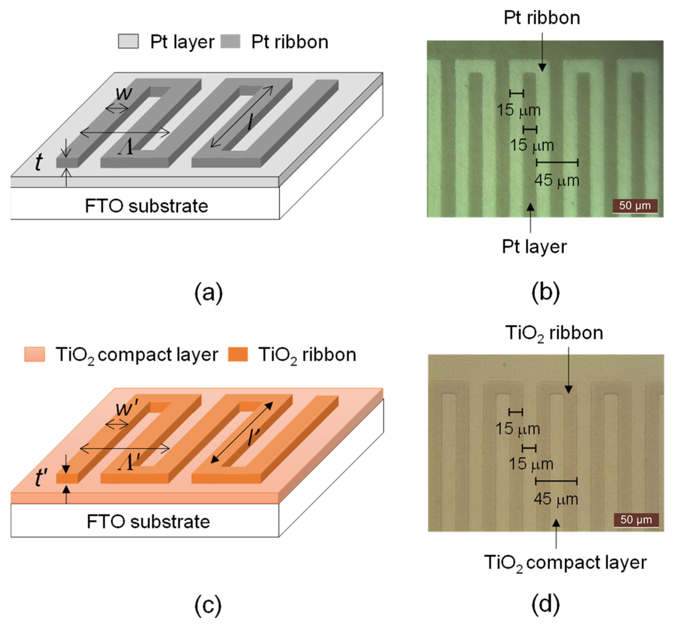
Figure 1a,b displays the schematic diagram and microscopic picture of a Pt ribbon that was deposited on a fluorine-doped tin oxide (FTO) glass substrate (Macro Fortunate, New Taipei City, Taiwan) with a 135-nm-thick Pt layer, respectively. The side length (sl), period (Λ), width (w) and thickness (t) of the Pt ribbon are 5 mm, 60 μm, 15 μm and 90 nm, respectively. The Pt ribbon, Pt layer and FTO substrate compose the counter electrode of the DSSC in this research.
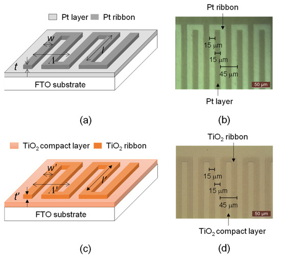
Figure 1.
(a) Schematic diagram and (b) microscopic picture of a Pt ribbon deposited on an FTO substrate with a Pt layer. (c) Schematic drawing and (d) microscopic picture of a TiO2 ribbon deposited on an FTO substrate with a TiO2 compact layer.
A EPG516 photoresist (PR) layer (Everlight Chemical, Taipei, Taiwan) was deposited on the FTO glass substrate with a 135-nm-thick Pt layer. The FTO substrate with the PR layer was put on a hot plate for soft baking. The image of the pattern of a mask was projected onto the PR layer after UV illumination. The irradiated PR layer was placed into EPD48 developer (Everlight Chemical, Taipei, Taiwan) for development, and then fixed in deionized water. The PR pattern was obtained after fixing. A CS-400 sputtering machine (Junsun Tech, New Taipei City, Taiwan) was used to deposit a 90-nm-thick Pt layer on the PR pattern. The sputtering machine has a Pt target (Well-Being Enterprise, Taipei, Taiwan) with a diameter of 2 inches in the vacuum chamber of the sputtering machine. The distance between the FTO glass substrate and the target is 15 cm, and the temperature of the substrate was held at 23 °C during the deposition of Pt. A sputtering power of 40 W was applied to the target and the pressure in the vacuum chamber was 7 × 10⁻³ torr during the deposition of Pt. The time for the deposition of Pt was 20 min in this study. A 90-nm-thick Pt layer was deposited on the PR pattern using the sputtering machine, and then the FTO glass substrate was immersed in acetone for removing the PR pattern. The Pt ribbon was obtained following the removal of the PR pattern.
Figure 1c,d displays a schematic drawing and microscopic picture of the TiO2 ribbon that was deposited on a FTO substrate with a 135-nm-thick TiO2 compact layer. The side length (l′), period (Λ′), width (w′) and thickness (t′) of the TiO2 ribbon are 5 mm, 60 μm, 15 μm and 90 nm, respectively. The TiO2 ribbon was fabricated by photolithography, sputtering and lift-off processes. The TiO2 compact layer not only facilitates the contact of a porous semiconductor layer and transparent conductive oxide layer but also prevents the contact of the transparent conductive oxide layer and the dye molecules [11,12].
A blade coater was used to coat a TiO2 paste layer (P300, Ruilong, Miaoli County, Taiwan), made of TiO2 nanoparticles with sizes ranging from 25 nm to 50 nm, on the TiO2 ribbon. To crystallize the TiO2 nanoparticles, the TiO2 paste layer was annealed by a chamber furnace (ELF, Carbolite-Gero, Hope Valley, England, UK). The temperature of the TiO2 paste layer was increased from 25 °C to 500 °C with a 5 °C/min interval, and was kept constant at 500 °C for 45 min. The TiO2 paste layer was cooled from 500 °C to 25 °C in the environment. The X-ray diffraction spectrum of the annealed paste layer reveals that the TiO2 nanoparticles have a crystallinity of 100% (data not shown).
D719 dye belongs to the first-generation of dyes used in DSSCs, and many researchers recognize it as a standard product. In addition, D719 dye is cheap and accessible. Therefore, D719 dye was used in this study. A N719 mixture was prepared by mixing 59.4 mg D719 dye (Merck, Taipei, Taiwan), 0.05 L acetonitrile and 0.05 L tert-butanol. Therefore, the N719 mixture had a 0.5 mM concentration in this study. The N719 mixture was stirred by a magnetic stirrer bar for 24 h. The TiO2 paste layer was places in this mixture for 30 h. The TiO2 compact layer, TiO2 ribbon, TiO2 paste layer and N719 mixture constitute the photoelectrode in this study.
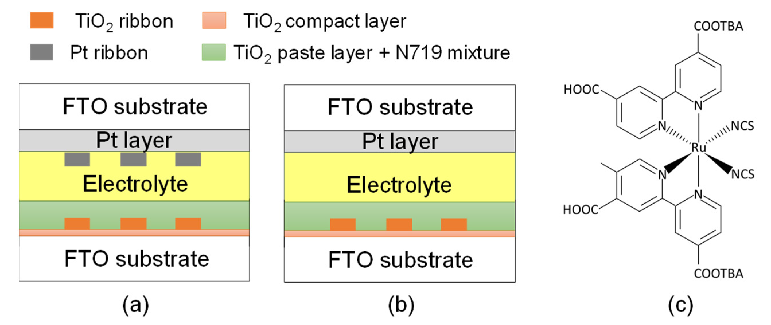
Figure 2a,b displays the configurations of DSSCs with and without a Pt ribbon, respectively. The photoelectrode and counter electrode create an empty cell with a gap of 20 μm. The TiO2 ribbon and Pt ribbon are aligned with each other. The empty cell was filled with an electrolyte (EL-200, Everlight Chemical, Tainan, Taiwan). The DSSC with the Pt and TiO2 ribbons was obtained following the filling of the electrolyte. The DSSC in Figure 2b exhibits the same structure as that in Figure 2a. However, the DSSC in Figure 2b does not have a Pt ribbon. A DSSC without a Pt ribbon was used to assess the photoelectric efficiency of the DSSC with the Pt ribbon. Figure 2c presents the structure of D719 dye.

Figure 2.
Configuration of DSSCs (a) with and (b) without a Pt ribbon. (c) Structure of D719 dye.
The amount of D719 dye adsorbed on the TiO2 paste layers of the DSSCs with and without the Pt ribbon were measured by ultraviolet-visible spectrometry [13]. The experimental results revealed that D719 dye has an identical adsorption amount of 0.34 mM in the DSSCs with and without the Pt ribbon, which is 69% of the concentration of the N719 mixture. The identical adsorption amount arises because the photoelectrodes are the same in the DSSCs with and without the Pt ribbon.
A JSM-6510 scanning electron microscope (JEOL, Tokyo, Japan) and an INNV2-BASE atomic force microscope (Bruker, Massachusetts, USA) were used to investigate the surface morphology of the counter electrodes of the DSSCs with and without the Pt ribbon. The incident photon-to-electron efficiency (IPCE) spectra of the DSSCs with and without the Pt ribbon were measured using an LSQE-N measurement system (LiveStrong Optoelectronics, Kaohsiung, Taiwan).
All the experiments in this study were performed on twenty DSSCs with Pt ribbons and twenty DSSCs without Pt ribbons. The experimental data in this study are the averages of the measured values of the DSSCs with and without the Pt ribbons.
3. Results and Discussions
Figure 3a,b displays the scanning electron microscopy images of the Pt ribbon that was deposited on the Pt layer at 0° and 45° incident angles, respectively. The Pt ribbon was successfully made by photolithography, sputtering and lift-off processes. The protrusive structure of the Pt ribbon increases the surface area of the counter electrode but also offers specific channels for directional electron transport. Figure 3c,d reveals the scanning electron microscopy images of the TiO2 ribbon deposited on the TiO2 compact layer at 0° and 45° incident angles, respectively. The protrusive structure of the TiO2 ribbon increases the surface area of the photoelectrode but also offers specific channels for directional electron transport.
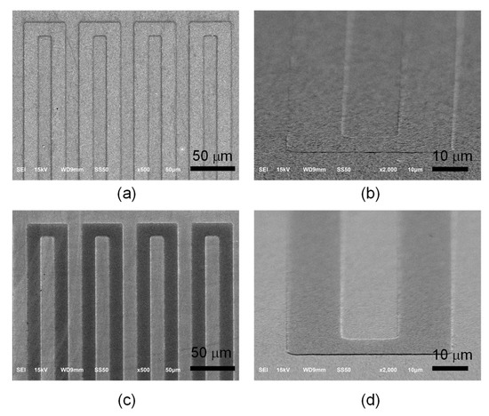
Figure 3.
Scanning electron microscopy images of Pt ribbon deposited on a Pt layer at (a) 0° and (b) 45° incident angles. Scanning electron microscopy images of TiO2 ribbon deposited on a TiO2 compact layer at (c) 0° and (d) 45° incident angles.
Figure 4a,b displays the top and side views of the atomic force microscopy images of the Pt ribbon deposited on the Pt layer, respectively. Figure 4c,d displays the top and side views of the atomic force microscopy images of the TiO2 ribbon deposited on the TiO2 compact layer, respectively. The results in Figure 4a–d show the actual relief of the surfaces of the Pt and TiO2 ribbons.
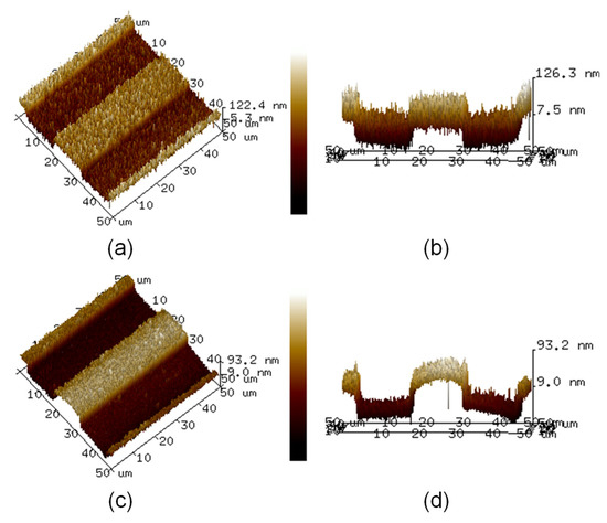
Figure 4.
(a) Top and (b) side views of atomic force microscopy images of Pt ribbon deposited on Pt layer. (c) Top and (d) side views of atomic force microscopy images of TiO2 ribbon deposited on TiO2 compact layer.
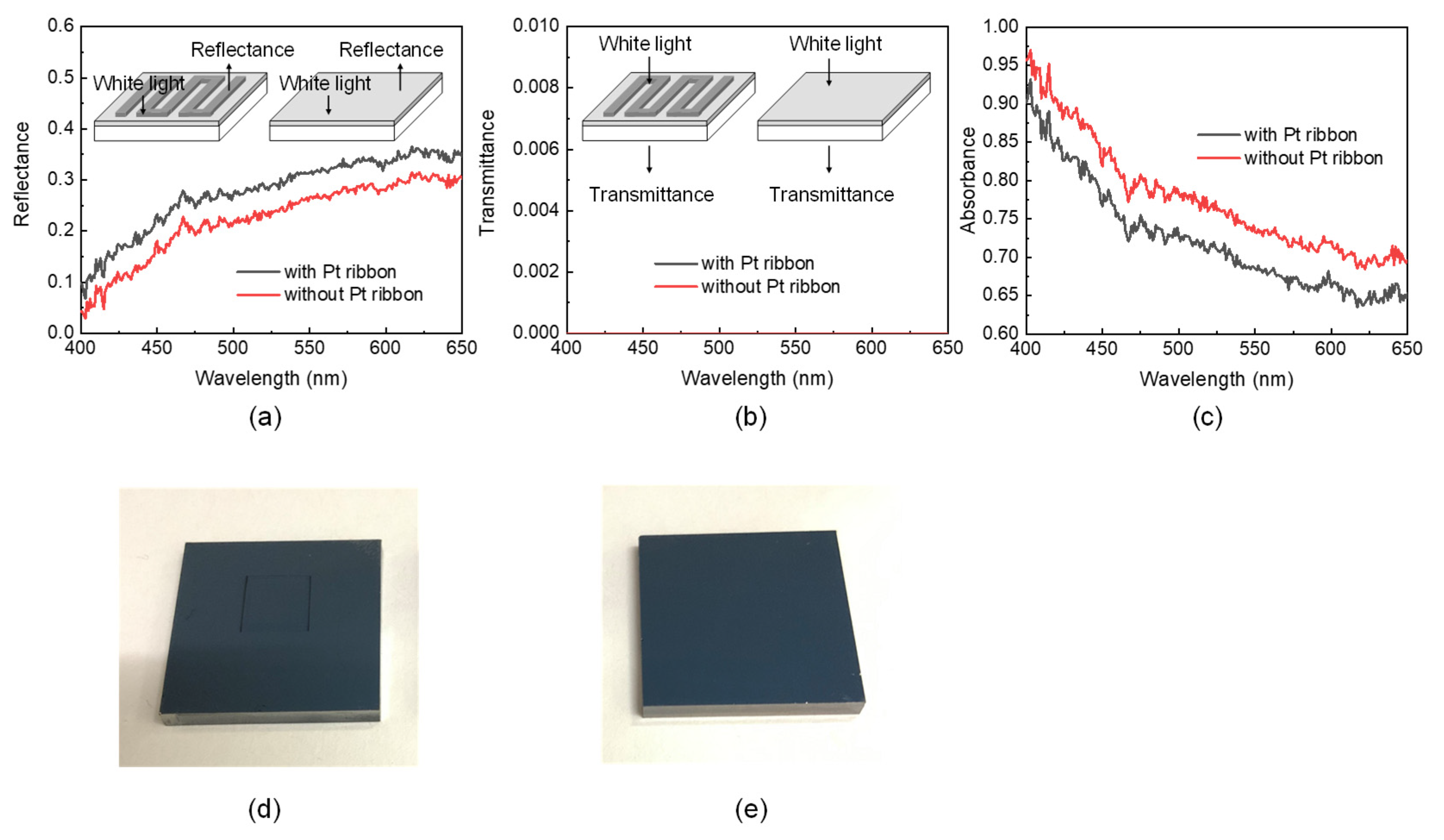
The insets of Figure 5a,b reveal the measurement of the reflection (transmission) spectra of the FTO substrates with and without the Pt ribbon. The spectra were obtained in an LSRT-R reflection and transmission system (LiveStrong Optoelectronics, Kaohsiung, Taiwan). The spectral resolution of the system was 1 nm, and its wavelength ranges from 300 nm to 900 nm. The light is normally incident from the side of the Pt ribbon (Pt layer) for measuring the reflection and transmission spectra of the FTO substrate with (without) the Pt ribbon. The reflection (transmission) of a white plate (air) is utilized to normalize those of the FTO substrates with and without the Pt ribbon.

Figure 5.
(a) Reflection, (b) transmission and (c) absorption spectra of FTO substrates with and without a Pt ribbon. Insets in (a)[(b)] present the measurement of the reflection (transmission) spectra of the FTO substrates with and without a Pt ribbon. Photos of FTO substrates (d) with and (e) without a Pt ribbon.
Figure 5a–c displays the reflection, transmission and absorption spectra of the FTO substrates with and without a Pt ribbon, respectively. The absorption spectra were obtained from Figure 5a,b via A + T + R = 1, where A, T and R are the absorbance, transmittance and reflectance of a material, respectively, at a particular wavelength. The FTO glass substrate with the Pt ribbon has a larger reflectance (smaller absorbance) at each of the wavelengths ranging from 400 nm to 650 nm than that without a Pt ribbon. This result implies that a DSSC with a Pt ribbon may have a larger photoelectric efficiency than a DSSC without a Pt ribbon because the Pt ribbon and Pt layer of the former reflect more incident photons back to the TiO2 paste layer than the Pt layer of the latter.
Each of the FTO substrates with and without the Pt ribbon has a 135-nm-thick Pt layer. Figure 5d,e presents photos of the FTO substrates with and without the Pt ribbon, respectively. The two FTO substrates appear black; thus, the Pt layers strongly absorb the incident light. The strong absorption of the Pt layers causes zero transmittance of the FTO substrates at each of the wavelengths ranging from 400 nm to 650 nm. The zero transmittance of the FTO substrates with and without the Pt ribbon implies that incident photons will not be removed from the counter electrodes of DSSCs with and without a Pt ribbon. The results in Figure 5a–c reveal that Pt ribbons may increase the photoelectric efficiencies of DSSCs.
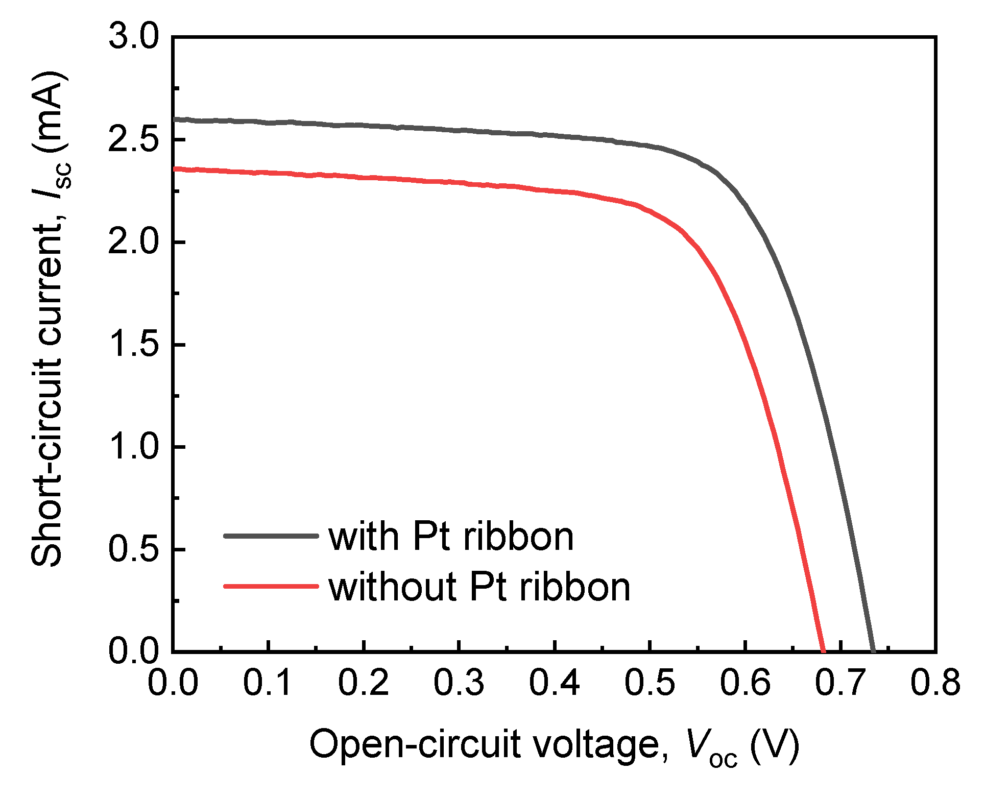
Figure 6 presents the dependencies of the short circuit currents (ISC) of the DSSCs with and without the Pt ribbon on the open circuit voltages (VOC). The ISC–VOC curves in Figure 6 were obtained using a AM 1.5 solar simulator (XES-40S2, San-EI Electric, Osaka, Japan) and a 2400 source meter (Keithley, Cleveland, OH, USA). The active area of each of the DSSCs with and without the Pt ribbon is 5 mm × 6 mm.
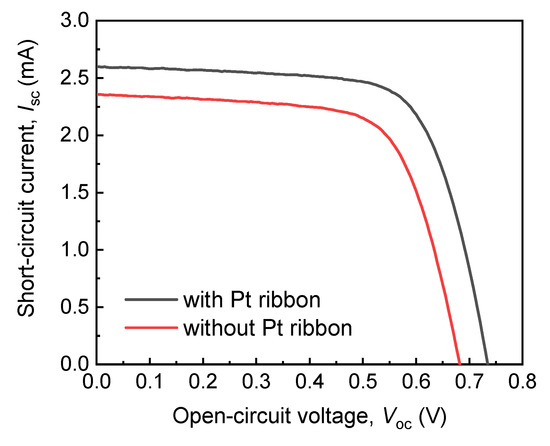
Figure 6.
Dependencies of short circuit currents (ISC) of DSSCs with and without a Pt ribbon on open circuit voltages (VOC).
Table 1 presents the open circuit voltages, short circuit currents, fill factors (FFs) and photovoltaic efficiencies of the DSSCs with and without a Pt ribbon. The DSSC with the Pt ribbon has a larger VOC, ISC and FF than that without a Pt ribbon. These results indicates that the photoelectric efficiency of the DSSC with the Pt ribbon exceeds that of the DSSC without a Pt ribbon by 21%. The large photoelectric efficiency of the DSSC with the Pt ribbon results from the protrusive structure of the Pt ribbon and specific electron transport channels of the structure.

Table 1.
Open circuit voltages, short circuit currents, fill factors and photovoltaic efficiencies of DSSCs with and without a Pt ribbon.
The fill factor is related to the series resistance and shunt resistance of a DSSC. The series resistance refers to the sum of the resistances that occur between the layers of a DSSC and at its external contacts. An increased series resistance will reduce the photovoltaic current in a DSSC, reducing the photovoltaic efficiency of the DSSC. To reduce series resistances, DSSCs must be designed with low material resistances and improved contact designs. The shunt resistance refers to the resistance that involves power losses due to the electron hole recombination in the manufacturing defects of a DSSC. A decreased shunt resistance will increase the recombination current in a DSSC, reducing the photovoltaic efficiency of the DSSC. To increase shunt resistances, DSSCs must be designed with few manufacturing defects. The series resistance and shunt resistance act in opposition, and the fill factor is a measure of how balanced they are within a DSSC.
The material resistances, contact designs and manufacturing defects were carefully controlled in the DSSCs with and without a Pt ribbon in this study. This fact reveals that the degree of the balance between the series resistance and the shunt resistance is similar in each of the cells. Therefore, the DSSCs with and without the Pt ribbon have similar fill factors. This result reveals that the photoelectric efficiencies of the DSSCs with and without the Pt ribbon change more significantly than their fill factors. Many other papers have also reported that the photoelectric efficiencies of DSSCs change more significantly than their fill factors [14,15,16].
Figure 7 displays the IPCE spectra of the DSSCs with and without a Pt ribbon. The DSSC with a Pt ribbon has a larger IPCE in the range of wavelengths studied here compared to the DSSC without a Pt ribbon. This result confirms the DSSC with the Pt ribbon has a larger short circuit current than that without a Pt ribbon due to , where JSC refers to the short circuit current density of a DSSC; q represents the charge of an electron; φ(λ) refers to the wavelength-dependent photon flux of incident light; and IPCE(λ) represents the wavelength-dependent IPCE of the DSSC.
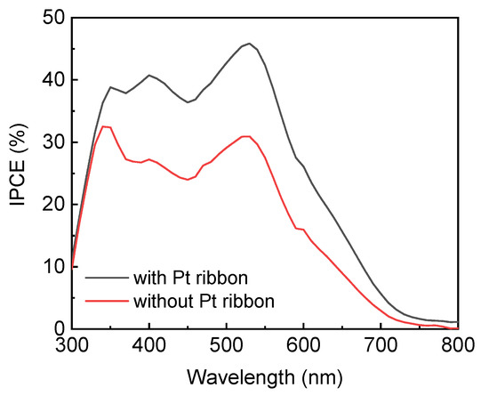
Figure 7.
IPCE spectra of DSSCs with and without a Pt ribbon.
The electrochemical impedance spectra of the DSSCs with and without a Pt ribbon were obtained from a ZIVE SP1 impedance analyzer (WonATech, Seoul, Republic of Korea) at a bias voltage of 10 mV and a solar intensity of 100 mW/cm2. Figure 8a,b displays the Nyquist and Bode plots of the DSSCs with and without a Pt ribbon.
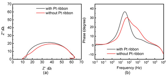
Figure 8.
(a) Nyquist and (b) Bode plots of DSSCs with and without a Pt ribbon.
The series resistances (Rs, Rct and Rrec), peak frequencies (fp) of the Bode plots and electron lifetimes (τ) for the DSSCs with and without a Pt ribbon are presented in Table 2. Rs refers to the series resistance related to the electron transport at the FTO/photoelectrode interface; Rct represents the series resistance related to the electron transport at the electrolyte/counter electrode interface and Rrec refers to the series resistance related to the electron transport at the photoelectrode/electrolyte interface. fp is the peak frequency of the second semi-circle of a DSSC from the Bode plot. τ is given by τ = 1/(2π × fp).

Table 2.
Series resistances (Rs, Rct and Rrec), peak frequencies (fp) of Bode plots and electron lifetimes (τ) for DSSCs with and without a Pt ribbon.
The DSSC with the Pt ribbon has a smaller Rct than that without a Pt ribbon. Therefore, the electron transport from an external circuit to the DSSC is more efficient in the DSSC with the Pt ribbon than in that without a Pt ribbon. The DSSC with the Pt ribbon has a larger τ than that without a Pt ribbon. As a result, the electron hole recombination is less likely in the DSSC with the Pt ribbon than in that without a Pt ribbon. The small Rct and large τ of the DSSC with the Pt ribbon reveal that the Pt ribbon increases the photoelectric efficiency of the DSSC. DSSCs with and without a Pt ribbon have similar Rs and Rrec, owing to their identical electrolyte layers and photoelectrodes.
4. Conclusions
This study develops a method for coating Pt ribbon onto an FTO substrate through photolithography, sputtering and lift-off processes. An FTO glass substrate without a Pt ribbon is fabricated to evaluate the performance of an FTO substrate with a Pt ribbon. The FTO substrate with the Pt ribbon has a large reflectance at wavelengths ranging from 400 nm to 650 nm compared to that without a Pt ribbon. This result implies that a DSSC with a Pt ribbon may have a larger photoelectric efficiency than a DSSC without a Pt ribbon because the Pt ribbon and Pt layer of the former reflect more incident photons back into the TiO2 paste layer than the Pt layer of the latter. The photoelectric efficiency (5.32%) of the DSSC with a Pt ribbon is larger than that (4.38%) of the DSSC without a Pt ribbon by 21%, not only because the protrusive structure of the Pt ribbon increases the surface area of the counter electrode, but also because it contains specific channels for directional electron transport. This result is confirmed by the electrochemical impedance spectra and the incident photon-to-electron efficiency spectra of the DSSCs with and without a Pt ribbon. Pt ribbon has potential in the development of next generation solar cells.
Author Contributions
Conceptualization, C.-Y.H.; methodology, W.-F.L.; validation, W.-F.L.; formal analysis, W.-F.L. and C.-Y.H.; investigation, W.-F.L., Y.-C.C., J.-H.Y. and C.-Y.H.; resources, W.-F.L., T.-F.L., J.-H.L., Y.-N.L., W.-H.L. and C.-Y.H.; data curation, W.-F.L., Y.-C.C., J.-H.Y., T.-F.L. and C.-Y.H.; writing—original draft preparation, W.-F.L. and C.-Y.H.; writing—review and editing, W.-F.L., W.-C.H., T.-F.L. and C.-Y.H.; visualization, W.-F.L., Y.-C.C., J.-H.Y. and C.-Y.H.; supervision, W.-C.H. and C.-Y.H.; project administration, C.-Y.H.; funding acquisition, T.-F.L. and C.-Y.H. All authors have read and agreed to the published version of the manuscript.
Funding
This research was funded by the Ministry of Science and Technology (MOST) of Taiwan under contract nos. MOST 111-2112-M-029-006 and MOST 111-2221-E-035-006.
Institutional Review Board Statement
Not applicable.
Informed Consent Statement
Not applicable.
Data Availability Statement
Data are contained within the article.
Conflicts of Interest
The authors declare no conflict of interest.
References
- Dürr, M.; Schmid, A.; Obermaier, M.; Rosselli, S.; Yasuda, A.; Nelles, G. Low-temperature fabrication of dye-sensitized solar cells by transfer of composite porous layers. Nat. Mater. 2005, 4, 607–611. [Google Scholar] [CrossRef] [PubMed]
- Lee, B.K.; Kim, J.J. Enhanced efficiency of dye-sensitized solar cells by UV–O3 treatment of TiO2 layer. Curr. Appl. Phys. 2009, 9, 404–408. [Google Scholar] [CrossRef]
- Li, Y.; Liang, C.; Wang, G.; Li, J.; Chen, S.; Yang, S.; Xing, G.; Pan, H. Two-step solvent post-treatment on PTAA for highly efficient and stable inverted perovskite solar cells. Photonics Res. 2020, 8, A39–A49. [Google Scholar] [CrossRef]
- Jia, Z.; Chen, Z.; Chen, X.; Yao, J.; Yan, B.; Sheng, R.; Zhu, H.; Yang, Y. 19.34 cm2 large-area quaternary organic photovoltaic module with 12.36% certified efficiency. Photonics Res. 2021, 9, 324–330. [Google Scholar] [CrossRef]
- Lai, W.F.; Chao, P.L.; Lin, X.Y.; Chen, Y.P.; Liu, J.H.; Lin, T.F.; Hsu, W.C.; Huang, C.Y. Characteristics of dye-sensitized solar cells with TiO2 stripes. Materials 2022, 15, 4212. [Google Scholar] [CrossRef] [PubMed]
- Hsu, C.P.; Lee, K.M.; Huang, T.W.; Lin, C.Y.; Lee, C.H.; Wang, L.P.; Tsai, S.Y.; Ho, K.C. EIS analysis on low temperature fabrication of TiO2 porous films for dye-sensitized solar cells. Electrochim. Acta 2008, 53, 7514–7522. [Google Scholar] [CrossRef]
- Wu, J.; Lan, Z.; Lin, J.; Huang, M.; Huang, Y.; Fan, L.; Luo, G.; Lin, Y.; Xie, Y.; Wei, Y. Counter electrodes in dye-sensitized solar cells. Chem. Soc. Rev. 2017, 46, 5975–6023. [Google Scholar] [CrossRef] [PubMed]
- Fang, X.; Ma, T.; Guan, G.; Akiyama, M.; Abe, E. Performances characteristics of dye-sensitized solar cells based on counter electrodes with Pt films of different thickness. J. Photochem. Photobiol. A 2004, 164, 179–182. [Google Scholar] [CrossRef]
- Özkan, M.; Hashmi, S.G.; Halme, J.; Karakoç, A.; Sarikka, T.; Paltakari, J.; Lund, P.D. Inkjet-printed platinum counter electrodes for dye-sensitized solar cells. Org. Electron. 2017, 44, 159–167. [Google Scholar] [CrossRef]
- Venkatesan, S.; Manurung, D.; Teng, H.; Lee, Y.L. Efficiency and stability improvements for room light dye-sensitized solar cells in the presence of electrochemically fabricated composite counter electrodes. J. Power Sources 2022, 518, 230781. [Google Scholar] [CrossRef]
- Liu, Q.Q.; Zhang, D.W.; Shen, J.; Lia, Z.Q.; Shia, J.H.; Chen, Y.W.; Sun, Z.; Yang, Z.; Huang, S.M. Effects of RF and pulsed DC sputtered TiO2 compact layer on the performance dye-sensitized solar cells. Surf. Coat. Technol. 2013, 231, 126–130. [Google Scholar] [CrossRef]
- Yu, H.; Zhang, S.; Zhao, H.; Xue, B.; Liu, P.; Will, G. High-performance TiO2 photoanode with an efficient electron transport network for dye-sensitized solar cells. J. Phys. Chem. C 2009, 113, 16277–16282. [Google Scholar] [CrossRef]
- Boruah, B.S.; Daimari, N.K.; Biswas, R. Functionalized silver nanoparticles as an effective medium towards trace determination of arsenic (III) in aqueous solution. Results Phys. 2019, 12, 2061–2065. [Google Scholar] [CrossRef]
- Pavasupree, S.; Ngamsinlapasathian, S.; Nakajima, M.; Suzuki, Y.; Yoshikawa, S. Synthesis, characterization, photocatalytic activity and dye-sensitized solar cell performance of nanorods/nanoparticles TiO2 with mesoporous structure. J. Photochem. Photobiol. A 2006, 184, 163–169. [Google Scholar] [CrossRef]
- Yang, J.H.; Bark, C.W.; Kim, K.H.; Choi, H.W. Characteristics of the Dye-Sensitized Solar Cells Using TiO2 Nanotubes Treated with TiCl4. Materials 2014, 7, 3522–3532. [Google Scholar] [CrossRef] [PubMed]
- Kathirvel, S.; Sireesha, P.; Su, C.; Chen, B.R.; Li, W.R. Morphological control of TiO2 nanocrystals by solvothermal synthesis for dye-sensitized solar cell applications. Appl. Surf. Sci. 2020, 519, 146082. [Google Scholar] [CrossRef]
Disclaimer/Publisher’s Note: The statements, opinions and data contained in all publications are solely those of the individual author(s) and contributor(s) and not of MDPI and/or the editor(s). MDPI and/or the editor(s) disclaim responsibility for any injury to people or property resulting from any ideas, methods, instructions or products referred to in the content. |
© 2023 by the authors. Licensee MDPI, Basel, Switzerland. This article is an open access article distributed under the terms and conditions of the Creative Commons Attribution (CC BY) license (https://creativecommons.org/licenses/by/4.0/).

