Abstract
This paper explores the synthesis methods and properties of vertically aligned graphene nanosheets (VG) and their applications. VG is obtained using the plasma-enhanced chemical vapor deposition (PECVD) method, and different VG types with other properties can be obtained by changing the process parameters. VG is part of the graphene family; properties such as excellent electrical conductivity, thermal conductivity, chemical stability, and a large, specific surface area make it suitable for biomedical applications. Examples of biomedical applications in which VG is used are biosensors, electrochemical sensors, modified surfaces for bone growth, regeneration, and for antimicrobial effects. First, VG’s properties are reviewed in this review article, and then the most recent progress in its applications and related sciences and technologies are discussed.
1. Introduction
Since 2010, when the Nobel Prize in Physics was awarded for discoveries regarding the two-dimensional material graphene, research on its properties has been extensive. Scientists have been committed to identifying its potential applications, which should prove advantageous over its competitors. This review article focuses on one particular class of graphene-containing complex material: vertical graphene (VG). VG consists of few-layer graphene-containing carbon nanosheets that grow perpendicular to the deposition substrate. The first observation of VG was made in 1997 when Ando noted “carbon roses” during the fabrication of carbon nanotubes [1] (see Figure 1 for the timeline of the discovered graphene). VG is a revolutionary new type of carbonic material that offers a range of benefits over traditional carbon-based materials. Its unique properties of increased strength, durability, and superior electrical and thermal conductivity make it an ideal choice for various applications, from electrical components and batteries to aerospace and automotive parts. Furthermore, thanks to its lightweight and low cost, vertical graphene’s potential for large-scale production opens up exciting possibilities for the future of materials science.

Figure 1.
Timeline of discovered graphene.
The morphology and structure of VG are of significant interest to researchers across various fields. This versatile material comprises graphite atoms arranged in a hexagonal lattice, with one carbon atom at each hexagon corner. As a two-dimensional sheet, graphene’s structure gives it unique electrical, optical, and thermal properties. When graphene is grown in a three-dimensional shape, its geometry can be manipulated to further enhance its unique characteristics [2]. This vertical arrangement allows researchers to explore and exploit the properties of graphene. A schematic representation of VG and its morphology and most essential features can be observed in Figure 2. Combining its intrinsic qualities with innovative external control will enable us to design and fabricate diverse hybrid materials with various properties and applications (see Figure 3).
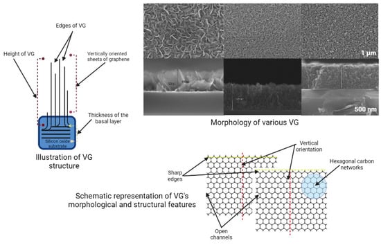
Figure 2.
Schematic representation of VG: structure (the way VG is growing), morphology (SEM images of various VG), and the most important morphological and structural features.
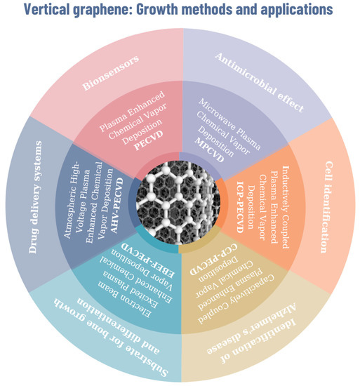
Figure 3.
Graphical interpretation of vertical graphene growth methods and potential applications in the biomedical domain.
The structure of VG on different substrates has been widely studied over the last few years due to its potential for various applications. The VG nanosheets are constructed from interconnected 3D porous networks of graphitic sheets that are aligned perpendicularly to the substrates. These sheets consist of 3–12 layers of graphene and are typically only a few micrometers in size [3]. This interconnected network is anchored onto a nanometer-thick layer of graphitic material that has been grown on the VG substrate interface, creating a unique and robust structure.
The carbon atoms are arranged in a hexagonal network, with each carbon atom covalently bonded to three other carbon atoms in the same plane. This arrangement of carbon atoms gives VG its characteristic honeycomb lattice structure. The structure of this lattice is highly ordered and provides VG with a remarkable combination of strength and flexibility.
The arrangement of the carbon atoms in vertically oriented graphene determines its electrical properties [4,5]. The electrons in the graphene lattice are free to move in two dimensions and create a highly conductive material. In the VG structure, the layers are held together by Van der Waals forces. This makes the layers more flexible, enabling greater control over the material’s properties. Furthermore, the vertical structure of graphene provides better support for functionalizing molecules, allowing for better electrical conductivity and increasing the chemical reactivity of the material. The structure of VG on different substrates has led to a wide range of potential applications, ranging from chemical sensors and nanoelectronics to composites for space applications. With further research, the use of vertical graphene may be further expanded and improved, leading to more effective materials and devices with increased performance [6,7]. The morphology of VG is one of the most critical aspects of its structure, and it is vital to appreciate its many uses fully. By understanding the structure and properties of this fascinating material, we can unlock its potential and benefit from its many advantages [4,5,6,7].
In the following two chapters, we review all available methods of obtaining VG and its applications in the biomedical domain. Then, we explore the potential of vertical graphene for further research in the biomedical field and its potential for further development. We also assess the challenges of obtaining vertical graphene and potential solutions. Finally, we provide an overview of the current opportunities to apply VG in the biomedical domain.
2. Growth Process of VG
Vertically oriented graphene is a robust material with remarkable properties and a wide range of potential applications. Its growth process involves a complex series of steps that start with depositing a thin layer of carbon atoms directly onto a substrate. Some researchers believe that the starting point for VG growth arises from the misalignment of graphitic layers in the “carbon onion” and/or the buffer layer, which acts as a nucleation center. The growth process continues with the adsorption of carbon atoms and their diffusion toward the edges of the sheets. At the same time, the amorphous carbon is removed by atomic hydrogen, either by dissociating the hydrocarbon molecules used as a precursor or by pure H2 added to the gaseous mix [8]. Depending on process parameters, additional nucleation sites can form on the surface of the vertical growing sheets, resulting in ramifications contributing to the growth of secondary or tertiary sheets.
The growth of VG is a complex process, and multiple approaches have been demonstrated to be successful. Numerous published works have reported detailed information on growth processes and associated trends. We will summarize some significant trends and provide qualitative analysis and comparisons to overview the emerging growth processes comprehensively. With this, we can accurately represent the current state of VG growth and its potential for future development.
Vertical graphene is a highly conductive form of graphene, capable of providing valuable information on materials and electronic device components. Obtaining VG can be achieved in several ways, including chemical vapor deposition (CVD) [9] and epitaxial growth [10]. Each method has its process parameters and requirements; thus, it is essential to select the best method for a given application. CVD is a process in which a volatile precursor is injected into a chamber, usually under a vacuum. The reaction chamber is then heated to a temperature that prompts the gas to decompose into a coating material, which then adheres to the material’s surface. Over time, the coating gradually covers the exposed portion of the material, ultimately forming a uniform layer. Scientists should be aware that this process occurs with time and exposure. The process parameters for CVD vary depending on the precursor, the substrate, and the desired thickness of the graphene film [11]. Epitaxial growth is the growth of a graphene film directly on the substrate. The substrate can be either single- or multi-layer graphene and is selected based on the characteristics of the graphene film. The process parameters for epitaxial growth include the type of substrate and the growth temperature range [12]. Researchers can better understand the material and its potential applications by understanding the various methods of obtaining VG and associated process parameters.
2.1. Plasma-Enhanced Chemical Vapor Deposition (PECVD) Method
PECVD is a powerful technique for obtaining high-quality, vertically aligned graphene. Through the use of this method, graphene films with good coverage, uniformity, and thickness can be created. Additionally, this method can be optimized to increase the deposition rate and reduce the growth temperature, making it suitable for various commercial applications [13].
The proposed phenomenological four-stage model of plasma-assisted growth of carbon nanostructures was based on experimental observations [14]. Reactive radicals/ions were formed when the hydrocarbon precursor dissociated under the plasma. The growth kinetics of the nanomaterials and the transport mechanisms of the plasma species in the Plasma-Enhanced Chemical Vapor Deposition (PECVD) process was studied by Muñoz and co-workers [15]. The plasma power, substrate position in the plasma plume, and composition of the feedstock gas all have an impact on the energy and density of the plasma species. In addition, the type of substrate and its temperature can play a significant role in the growth process and, ultimately, lead to different morphologies and structural quality [14]. Therefore, these key factors can critically influence the final nanomaterial structures.
Concerning PECVD, the typically accepted process of VG growth is widely seen to involve three fundamental, consecutive stages: nucleation, growth, and termination [3]. The processes involved in VG growth can be summarized as follows: Firstly, nucleation takes place where defects on the substrate surface serve as a starting point for the growth of a buffer layer for any subsequent VG development. Next, growth occurs as graphenic nanosheets are pushed upwards due to stress and/or a localized electric field and carbon atoms consistently add to the exposed edges of the vertical-based graphene structure. Finally, termination takes place when the plasma’s depositing and etching abilities become equal, and VG growth is concluded as the exposed edges are covered [16]. A schematic growth process of VG on a silicon oxide substrate using the PECVD method is presented in Figure 4.
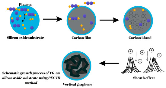
Figure 4.
A schematic growth process of VG on a silicon oxide substrate using the PECVD method.
A layer of either amorphous carbon (a-C) or carbide is commonly created in the nucleation stage and is known as a buffer layer [17,18]. The amorphous carbon layer comes from the contrast in the lattice parameters between the graphite and the substrate material. When carbon atoms react with or dissolve into the substrate, this triggers the formation of a carbide layer [16]. Within the structure, a flat or layered graphitic structure can be observed nestled between the amorphous carbon buffer coating and the perpendicular graphene nanosheets. Surrounding the growth of graphene nanosheets is a protective buffer layer that nullifies any substrate-dependent features that could interfere with uniform morphology. Removal of this buffer layer, achievable through etching techniques such as H or OH radicals, benefits the growth of VG nanosheets [19]. Even though vertically grown graphene (VG) nanosheets have a consistent morphology, the reasons behind this are due to three main factors: electric field, internal stress, and anisotropic growth impacts. The creation of the buffer layer and nucleation sites support the VG nanosheet’s unique vertical direction, which distinguishes it from other film formations, such as multi-walled CNTs or MWCNTs.
Hiramatsu [20] proposed a theoretical model of the VG mechanism of growth using the PECVD method, and it is based on five steps:
- (1)
- The formation of a very thin amorphous carbon layer induced by hydrocarbon radicals (CH4) adsorbed on the substrate followed by ion irradiation to form dangling bonds on the growing surface, resulting in the creation of nucleation sites;
- (2)
- The formation of nano-islands with dangling bonds due to the migration of adsorbed carbon species on the surface;
- (3)
- The adsorption of CHx radicals on the surface enhanced by ion irradiation;
- (4)
- The formation process involves the nucleation of small and disordered nanosheets of graphene at the location of these dangling bonds. This is then accompanied by two-dimensional expansion, which results in the creation of nano-graphene sheets with a haphazard orientation;
- (5)
- When considering nucleated graphene sheets with varying orientations, those that are nearly vertical to the substrate are more likely to grow faster into vertically standing nanosheets, owing to the electromagnetic fields that are produced by the plasma.
When the growth process is prolonged, the vertical nanowalls that are growing will intersect, leading to the formation of interconnected nanowalls similar to a labyrinth. As the growth period continues, the space between the top of these nanowalls gradually increases, leveling out at a certain point and forming two-dimensional graphenic sheets standing vertically on a substrate, with a high aspect ratio known as vertical graphene (VG) [20]. Figure 5 presents the working principle of the PECVD process.
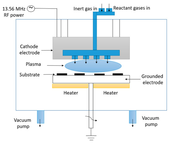
Figure 5.
Working principle of the PECVD process.
2.1.1. Microwave Plasma-Enhanced Chemical Vapor Deposition (MPECVD) Method
MPECVD was the first method employed to synthesize VG and is also commonly used to generate diamonds and carbon nanotubes. There are three kinds of microwave plasma—TE (transverse electric) Mode, TM (transverse magnetic) Mode, and ECR (electron cyclotron resonance) Mode—based on the microwave’s propagation characteristics. In the TE Mode, the electric field runs at a right angle to the propagation direction. As a result, the charged particles move in a direction that is perpendicular to the substrate plane. When operating in TM Mode, the magnetic field and direction of propagation are at right angles to one another, while the electric field runs parallel. This causes the electrons and ionized carbon radicals to move within the surface plane of the substrate in a microwave time scale. In the presence of ECR, the characteristics of electron transport transform into tensors and functions that hinge on the static magnetic flux intensity. This leads to a three-component vector motion of electrons and ionized carbon radicals [21,22,23].
Wu et al. [21] used the MPECVD method to grow carbon nanowalls. This system has a vertical quartz tube in a microwave cavity with a 500 W microwave source. The gases used are mixtures of CH4 and H2. An important parameter affecting carbon nanostructure growth is the H2/CH4 flow rate ratio. In this study, the researchers tested the growth of carbon nanowalls at different H2/CH4 flow rate ratios. They found that any growth with an H2/CH4 flow rate ratio > 50 for 5 min is difficult to obtain. When they reduced this ratio to 30, some amorphous carbon was formed. After many tests, they found that pure carbon nanowalls were received when the gas flow rate ratio was 4–8. The carbon nanowalls grew very fast and had a height of approximately 2 µm, and the width of the nanowall was in the range of 0.1–2 µm.
In 2005, Tanaka et al. [24] reported the growth of VG on a SiO2 substrate by microwave plasma-enhanced chemical vapor deposition. The researchers examined the propagation of the vertical grating (VG) over a SiO2 substrate and discovered that it did not need a catalyst, unlike the procedure of Wu et al. [21]. Furthermore, the investigators observed that the height of VG increased according to the square-root law as it was developed in time; high growth speeds of approximately 10 μm per hour were accomplished. In addition, they found that a valuable gas blend comprising hydrocarbons and hydrogen was employed.
2.1.2. Inductively Coupled Plasma-Enhanced Chemical Vapor Deposition (ICP-PECVD) Method
Scientists can generate inductively coupled plasma (ICP) through RF magnetic fields created by the water- or air-cooled copper coils. This mode is suitable for numerous carbon sources, and the frequency is usually between the tens of kHz to the tens of MHz. The most popular frequency used in industrial and research settings is 13.56 MHz RF. For ICP mode, ionized carbon radicals have the same direction as the current in the coil. This kind of plasma generation usually has two approaches, namely, planar ICP and tube/cylinder ICP, and each has its structure. In common practice, both planar inductively coupled plasma (ICP) and tube/cylinder ICP involves the movement of ionized carbon radicals parallel to the substrate plane [25]. Researchers have gradually devised new techniques for synthesizing VG, employing various carbon sources and variant growth strategies. For example, Seo [26] described a synthesis procedure that utilizes honey as the solid carbon source, a combination of argon and hydrogen as the buffer gas, and ICP-PECVD as both the growing system and heating source for the substrate.
Zhu et al. [27] grew carbon nanosheets using the RF-ICP-PECVD method. They used CH4 as a carbon source with a concentration of 40% in the H2 atmosphere. The process parameters for the growth of carbon nanosheets were as follows: pressure of 90 mTorr and RF power of 900 W at a temperature of 680 °C. This group obtained free-standing carbon nanosheets with thicknesses less than 1 nm without any catalyst or special substrate treatment. They could grow carbon nanosheets on different substrates such as Si, SiO2, W, Mo, Cr, Ta, Ti, and many others. Another research group reported the growth of carbon nanowalls using RF-ICP-PECVD and a mixture of CH4 and Ar. Hishikawa et al. [28] obtained carbon nanowalls with a relatively smooth surface using the following process parameters: pressure of 10–60 mTorr, temperature of 700–850 °C, RF power of 500 W, and flow rates of CH4:Ar at 7:1.4 sscm. In 2017, Cuxart et al. [29] used the ICP-PECVD technique to grow VG. They reported several advantages of this method: (a) during the catalyst-free growth of graphene nanosheets, the electric fields from the plasma were minimized; (b) it obtained VG with low defect density; (c) the growth temperature was reduced; and (d) the gas dissociation process was decoupled to allow better deposition of the graphene nanosheets on the substrate. Thus, it is considered that this method allows better control over the growth parameters and precursor gas, leading to better control over the shape and size of the nanostructures.
2.1.3. Capacitively Coupled Plasma-Enhanced Chemical Vapor Deposition (CCP-PECVD) Method
The development of capacitively coupled plasma (CCP) involves energizing one capacitor plate through RF power or DC voltage while the other plate remains either grounded or unconnected. Integrating CCP with different types of plasma, such as ICP and surface wave sustained plasma (SWP), creates VG, which leads to increased growth rates but also increases procedure complexity. Moreover, researchers have noted that CCP stimulates ionized carbon radicals to move perpendicular to the substrate plane in experimental settings [30,31].
In 2005, Shiji et al. [31] announced the successful creation of VGs, also known as carbon nanowalls (CNWs). These were made using CCP-PECVD, a process that uses fluorocarbon/hydrogen mixtures and radio-frequency plasma to deposit the material on the desired substrate. An investigation was conducted to assess the correlation between the expansion of VG and the conditions of its production, specifically, the diverse gaseous sources of carbon. Additionally, the study analyzed the impact of plasma’s hydrogen-atom density on VG’s expansion process by employing vacuum ultraviolet absorption spectroscopy.
Compared with ICP, CCP, with its parallel-plane geometry, has a more straightforward setup and can operate at higher pressures. However, its relatively low electron density and energy typically make it an insufficient plasma source to grow high-quality VG sheets. In fact, Langmuir probe measurements have found the plasma density and electron temperature of CCP to be approximately 109–1010 cm−3 and 1011 cm−3 for high-frequency CCP, respectively—much lower compared to other high-density plasma sources such as MW and ICP, which can reach densities from 1010 to 1012 cm−3 and 1013 cm−3, respectively [32,33]. Additionally, the high sheath potentials of CCP can damage surface bonds and further hinder the quality of crystals cultivated. Contamination from electrodes is also a potential issue. Therefore, incorporating a nanostructured catalyst was essential for the successful growth of VG when using CCP as an independent plasma source in a combination of an expanding RF plasma and magnetron sputtering setup. This setup allowed the electron density to reach levels of 1011 cm−3. This is the only successful application of CCP in this context [34,35].
2.1.4. Atmospheric-Pressure High Voltage-Enhanced Chemical Vapor Deposition (AHV-PECVD) Method
AHV-PECVD also causes the carbon radicals to move perpendicularly to the substrate surface, though it is typically challenging to grow VG on a large substrate [36]. Bo et al. [36] conducted a rapid synthesis of VG using AHV-PECVD. This research thoroughly outlines a unique reactor structure to manufacture VG sheets in a steady, homogenous production set up by the atmospheric pressure of the PECVD process. Furthermore, they explain the particular experiment executed with a U-shaped reactor design, which entails “dynamic mode” growth (as the metallic substrate is switched between rotational and axial motion during production) and shows the facets it has in comparison to the “static mode” reactor, which keeps the substrate in a fixed position.
2.1.5. Electron Beam Excited Plasma-Enhanced Chemical Vapor Deposition (EBEP-PECVD) Method
The EBEP-PECVD system is a unique fusion of DC discharge and electron extraction/acceleration methods, which facilitates the creation of plasma. The LaB6 disk cathode plays a crucial role in sustaining the DC discharge plasma by extracting electrons and propelling them towards the EBEP zone via a set of multi-hole grids. Unlike other synthesis methods, such as magnetron sputtering, TCVD, and HWCVD, the ionized carbon radicals produced here move mainly perpendicular to the substrate under the influence of the applied electric field. Furthermore, this plasma density is related to the pressure of the atmospheric environment and is consequently much higher than that of lower-pressure systems in a vacuum system [22,37].
Other studies for methods of growing VG include Guo et al.’s [38] discovery of a furnace that generates ionized carbon radicals for VG growth by thermally dividing CH4 at temperatures between 800 and 900 °C, also referred to as thermal chemical vapor deposition (TCVD), and Zheng et al.’s [39] explanation of a thermal decomposition procedure utilizing a 1600 °C SiC substrate for VG development. Additionally, there are other techniques, such as magnetron sputtering and thermal hot wire chemical vapor deposition (HWCVD), that have been described. It is important to note that the production of VG is influenced by two crucial plasma parameters: the movement of charged particles and the density of the plasma.
In the following table (Table 1), we present some other examples of growth methods and the parameters used for obtaining VG.

Table 1.
VG growth methods and process parameters.
3. Applications of VG
The evolution of vertical graphene for different applications is an exciting area of research. From lightweight, high-end materials for aerospace to energy storage breakthroughs, vertical graphene has become a material of increasing interest in material science. With its extraordinary physical, electrical, and optical properties, vertical graphene has been used to develop novel technologies and products with a wide range of applications, such as high-strength composites, flexible electronics, and energy storage devices. As research progresses, we observe vertical graphene’s evolution in applications that can help the environment, enhance safety, improve medical care, and more (see Figure 6). This area of research is advancing rapidly and stands to improve our lives in the near future drastically. Graphene, especially VG, has become a powerful tool in many domains, and its applications in the biomedical field are up-and-coming. In this chapter of the study, we focus on how vertical graphene can be used to advance biomedical research further and develop treatments for diseases. We discuss the potential of vertical graphene for creating more innovative devices and materials and pioneering therapies and regenerative medicine. The possibilities are endless, and the potential to revolutionize medical care is immense.
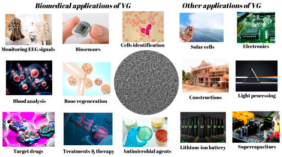
Figure 6.
Examples of applications in which VG could be successfully used.
VG has recently emerged as a powerful tool in the biomedical domain, bringing various innovative technologies to medicine. Applications of vertically oriented graphene for biomedical uses include the following: (1) Developing personalized medical treatments—by utilizing VG technology, treatments can be tailored to the individual, providing more tailored care to those in need. (2) Creating biosensors—graphene-based biosensors can be used to detect various key biological markers to provide more comprehensive, sensitive, and cost-effective healthcare solutions. (3) Enhancing delivery systems—graphene nanomaterials can be applied to delivery systems to improve cargo-lock and release precision, allowing drugs to be administered more quickly and with much higher accuracy. (4) Prosthetics—graphene-based prosthetics are beginning to revolutionize the way people with disabilities interact with the world around them. Using artificial muscles and skin-adaptive graphene technology, prosthetic users could regain some of their natural movement [47]. By leveraging the power of vertical-oriented graphene, a wide variety of new biomedical treatments and technologies are becoming available. These advancements bring better, more effective healthcare solutions to those needing them [48,49].
3.1. Biological Affects and Activity
According to the experiments conducted by Al-Jumaili et al. [48] in 2017, VG has an antimicrobial effect on certain microorganisms through interactions that occur in cell membranes. Previous studies have demonstrated that exposure to graphene can physically damage microorganisms through two possible pathways: insertion and cutting of the cell membrane and extraction of phospholipids from the lipid membrane. The dynamic simulation revealed that when a VG nanosheet is located 3.5–4.7 nm above bacterial membranes, it vibrates back and forth for 10–100 nanoseconds and penetrates the cell walls due to the powerful Van der Waals interaction and hydrophobic effects. Additionally, it has been suggested that graphene nanoparticles effectively strip phospholipids from the lipid barriers of the membranes. The extraction of phospholipids causes lipid breakage and cell membrane distortion caused by solid interaction forces from graphene nanosheets, leading to the irreversible destruction of living systems. Interactions occur between the surface of the graphene nanosheet and bacteria [48].
In 2018, Borghi et al. [49] conducted a study using VG as a bone growth and differentiation substrate. To obtain GNW, they used the PECVD method. Additionally, in this study, they tested the toxicity of graphene and observed that VG is biocompatible if it is transferred onto glass or silicon. Thus, the effect of graphene films on cellular response was tested using osteoblasts (Saos-2 cell line: human bone cells) and mesenchymal stem cells (MSC) in order to achieve an application in bone regeneration. The vertical orientation of graphene has some advantages: it can bind critical biological molecules, it has specific properties of graphene materials, and it can provide cell topographic information. The study demonstrated that human bone cells from a culture could attach and grow on the surface of VG. Compared to the specialized blades on which this type of cell develops, VG had 75% adherence and proliferation. Thus, the conclusion was that the surfaces coated with graphene were biocompatible and that the topography of the coating could have a profound influence on the long-term behavior of the cells, especially the process of cell differentiation and mineralization involved in the generation of bone cells (osteogenesis) [49].
The work reported by Al-Jumaili et al. [50] investigated VG’s physical bactericidal mechanism towards pathogenic bacteria, such as gram-negative cell Escherichia coli and gram-positive cell Staphylococcus aureus, by fabricating graphene with different edge densities. The VG, achieved through a catalyst-free, single-step PECVD system, displayed hydrophobicity and high roughness. Furthermore, its efficacy against specific human pathogens was established via its ability to act as an edge that breached and thus damaged the bacterial cell membrane [50].
Boonkaew et al. [51] demonstrated the viability of a boron/nitrogen co-doped diamond graphene nanowall (DGNW) and a screen-printed graphene electrode (SPGE) combination for the detection of serotonin (5-HT). Compared to the bare SPGE, the DGNW-modified electrode offered enhanced electrochemical performance and increased resistance to contamination in assessing neurotransmitter concentrations. Employing differential pulse voltammetry (DPV), the electrode registered a linear response above 1 and up to a 500 μM 5-HT concentration (R2 > 0.99), with a lower detection limit at 0.28 μM. Applying the setup within a synthetic urine sample also verified its practicality in a natural setting. All in all, the DGNW-modified electrode was shown to be an effective, anti-fouling alternative for electrochemical transduction [51].
3.2. Biosensors
VG provides a powerful platform for the development of biosensors and electrochemical biosensors. Its structure allows for highly sensitive signal capture and transduction, resulting in an outstanding performance in medical diagnostics and environmental monitoring applications. Sensors, biosensors, and electrochemical biosensors generally consist of a receptor and a transducer. The receptor, an organic or inorganic material, interacts specifically with specific target molecules that may be organic, inorganic, or entire cells. The transducer, part of the sensor, transforms the chemical information into a detectable output [52]. Graphene nanomaterials function as transducer biosensors, translating interactions between the receptor and target molecule into a measurable signal. VG has been used to make different biosensors due to the large surface area, electrical conductivity, high electron transfer velocity, and immobilization capability of various molecules. Various methods can accomplish the detection of target molecules. Electrochemical detection is the most popular technique employed today, which relies on conformational changes observed at the electrode/electrolyte interface to assess any biochemical or electrical modifications [53]. This method is based on the binding of the antibody and the antigen. The biosensors in this process require a working electrode (where the reaction occurs), a reference electrode (to complete the electrical current pathway between the two electrodes), and a counter electrode. Electrochemical sensors utilize current, potential, and resistance measurements, enabling the transducer to identify alterations in the electric signal resulting from target molecule-binding reactions [54]. The electrochemical detector detects changes in voltage, current, or impedance caused by various electrochemical characteristics, including electron reduction, conductivity, or capacity changes resulting from DNA hybridization or the oxidation of adenine (A), thymine (T), cytosine (C), and guanine (G) molecules in the DNA structure. These electrochemical signals that are created by the biosensors are assessed with the utilization of cyclic voltammetry (CV), differential pulse voltammetry (DPV), or electrochemical impedance spectroscopy (EIS) [55]. In the electrochemical approach, DNA immobilization is mediated by π-π interactions on the surface of graphene nanomaterials. Graphene margins, functional groups (carboxyl, hydroxyl, and epoxide) of graphene oxide, and reduced graphene oxide may also covalently interact with DNA [56]. In a study, a DNA sensor was investigated to detect double-stranded DNA (dsDNA) with a sensitivity of 10 fM to 10 mM, using the sharp and active edges of reduced graphene nanowalls (RGNW). The authors of this study suggested that the sharp and active edges of RGNW may facilitate the transfer of electrons between DNA and electrodes [57]. The sensor’s detection and sensitivity level can vary greatly depending on the target material. For instance, when detecting dsDNA, VG (also known as graphene nanowalls or GNW) has been found to be the optimal material, capable of detecting levels as low as 0.1 μM, as documented in the literature. In the case of catenary DNA (ssDNA), the gold nanoparticle modification of graphene oxide sensors increases the sensitivity for low detection limits of 0.005 fM [57].
In a 2013 study, Mao et al. developed a sensitive and selective vertical graphene field-effect transistor biosensor. They used the PECVD method to grow the VG directly on the sensor electrode. The FET biosensor detected protein by gauging adjustments in its electrical signal triggered by the connection between the antibody and the antigen. This group of researchers proved that the biosensor exhibits remarkable sensitivity (as low as ~2 ng/mL or 13 pM) and specificity specifically towards designated proteins [58].
In 2017, Qianwei et al. [59] developed a flexible electrochemical biosensor based on vertical graphene to determine real-time lactic acid levels in various probes. It has potential in clinical analysis, sports medicine, and the food industry. First, the PECVD method obtained the VG on a copper substrate. Next, copper was corroded in Fe(NO3)3 and 5% HCl to remove Cu and Fe nanoparticles together. The next step was to wash the substrate with deionized water and transfer the graphene sheet to a PET (polyethylene terephthalate) substrate. Before the biosensor electrodes (counting, working, and reference) were printed, the graphene transferred to the PET substrate was treated with oxygen plasma to improve its hydrophilicity (O2 10 sccm, pres. 0.2 mbar, RF 50 W for 3 min). Next, the working electrode was functionalized with L-lactate oxidase and coated first with chitosan and then with glutaraldehyde; the drying process was carried out at room temperature. Following the measurements, it was concluded that the flexible electrochemical biosensor had excellent sensitivity, specificity, stability, and flexibility [59].
VG has been used in various applications, for example, as material for improving the interfacial strength of composites or for enhancing the electrochemical capacities of electrodes when deposited on the surface of the electrode. In addition, applications involving combining VG with other nanostructures, such as nanoparticles, or in conjugation with soft materials, such as polydimethylsiloxane (PDMS), have been reported for improved performance. However, minimal therapies are dedicated to therapeutical implementation or, most importantly, effectively monitoring chemotherapeutic drugs.
In the study from 2018, Tzouvadaki et al. [60] achieved an ultrasensitive detection method for etoposide, one of the primary drugs used in cancer chemotherapy, reaching a detection limit (LOD) of up to 4.36 nM by using VG. This experiment was based on an electrochemical sensor, with electrodes made from VG on Si, SiO2, and Ni substrates and incubated in 10 mL of 200 mM PBS (phosphate buffer) to perform electrochemical measurements. The reference substance was ferrocyanide/ferician, an electroactive substance often used to calibrate electrochemical sensors. From the characterizations made on the three cases—VG on substrate Ni, Si, or SiO2—the best electrode version was that on the SiO2 substrate, having optimal performances for the electroactive components. This improved electrochemical performance of the biosensor could also be attributed to the large surface and good electrical conductivity of graphene nanostructures. Moreover, the LOD obtained in this paper suggests better performance than other biosensors based on graphene nanostructures for other known electroactive drugs [60].
Tincu et al. [61] reported a biosensor based on vertically-oriented nanosheets overlaid onto conductive interdigitate electrodes modified with anti-EpCAM antibodies. Through a correspondent assessment of the Bode and Nyquist diagrams, such as charge transfer resistance and double electrical capacity, exchange coefficients and Debye length, characteristic relaxation times of mobile charges, and alterations in permittivity, they could differentiate the signature of three types of tumor cells. Using the evaluation method, they reported that the permittivity of 1 MHz was 6.9 nF for MCF-7 cells (human breast cancer), 4.97 nF for HT-29 cells, and 3.63 nF for SW403 cells (two colorectal adenocarcinoma cell lines). Analysis of the electrochemistry has demonstrated the successful functioning of the VG-based electrochemical biosensor in detecting low concentrations (100 cells/mL) of tumor cells on the electrode surface [61].
The study conducted by Burinaru et al. presented a microfluidic device as a promising tool for circulating tumor cell (CTC) detection, quantification, and characterization. A means of detecting CTCs using a microfluidic device and an electrochemical impedance spectroscopy biosensor has been developed that does not require a label and can capture and measure these cells. The antibody-functionalized sensor was designed to detect specific molecules that are typically present in circulating tumor cells (CTCs) while being absent in normal blood cells. The two antibodies utilized were anti-EpCAM and anti-CD36. The efficiency of the microfluidic device was then tested on blood samples obtained from canines dealing with mammary carcinomas, as well as on MCF-7 breast cancer cells. The sensor had a sensibility to the adherence of circulating tumor cells (CTCs), with the capability of identifying the presence of just three MCF-7 cells on its surface [62].
In a study by Yao, vertically oriented graphene arrays (VGAs) were integrated into an application for electronic skin (e-skin), which has potential in prosthetics, soft robotics, wearable equipment, and medical monitoring. By submerging a natural latex film into a dispersion of cyclohexane, VGAs were grown directly on its surface. This led to nonstationary vertical graphene arrays that allowed the e-skin to sense even the slightest changes in pressure and airflow. In addition, the VGAs’ movement across an object’s surface allowed for differentiation in its shape. The electronic skin also boasts exceptional sensitivity to both light and heat, incredibly fast reaction times (6.7 milliseconds), and good durability (13.4 milliseconds). Additionally, its pressure sensing range extends from 2.5 Pa to 1.1 MPa, with a high sensitivity of 2.14 kPa−1 and robust cyclability of up to 2000 cycles. The e-skin is capable of detecting strains ranging from 0.5% to 250%, making it a strain sensor. It also boasts a hypersensitive perception of pressure and airflow, even when subjected to a 50% strain. Additionally, the e-skin is equipped with multiple sensing capabilities that enable it to detect an array of human or robotic motions, ranging from subtle to more obvious movements. By fabricating flexible, vertically-aligned graphene arrays onto a sheet of film, a method can be developed that can serve as an artificial skin to mimic the senses of human skin [63].
A study conducted by Yang et al. [64] presented a vertical graphene-based flexible piezoresistive sensor for routine measurements such as radial and carotid pulses and respiratory rate. The information obtained through the usage of this specific sensor was employed to assess heart rate, its regularity, and the rate of breathing for the purpose of detecting potential hazards such as reduced heart rate, irregular heart rhythm, heart-stopping, and arterial hardening in the individuals observed. Additionally, the easily accessible, non-invasive technology is well-suited for usage in large communities as it assists in promoting awareness about the significance of monitoring vital signs [64].
Chen conducted research whereby an electrochemical immunosensor using a gold-vertical graphene/TiO2 nanotube electrode (Au-VG/TiO2) that did not require any label was developed. The main purpose of this immunosensor was to accurately measure CA125, which is traditionally known as a marker for ovarian cancer. The Au-VG/TiO2 electrode served as the means to boost the signal, with cytosine and dopamine functioning as probes for oxidation and reduction channels, respectively. The VG nanosheets underwent synthesis on a TiO2 nanotube array through chemical vapor deposition (CVD). In addition, Au nanoparticles were embedded profoundly on the surface and in the root of the VG nanosheets through electrodeposition. The electrode surface was utilized for the direct immobilization of the CA125 antibody, taking advantage of its inherent attraction to Au nanoparticles. The successful detection of CA125 in human serum was accomplished using the immunosensor. The spiked serum samples exhibited recoveries ranging from 99.8 ± 0.5% to 100 ± 0.4% [65].
A team of researchers developed a compact, electrochemical sensing platform for the point-of-care detection of AD (Alzheimer’s disease) biomarkers in blood. This portable platform incorporates a working electrode with nanoAu-modified vertical graphene (VG@Au), which offers higher sensitivity, reduced detection limit, enhanced electrical conductivity, stability, and biocompatibility. In addition, the tau protein was assessed in the developed platform as a critical AD marker. The results demonstrated a linear range from 0.1 pg/mL to 1 ng/mL, with a detection limit of 0.034 pg/mL (S/N = 3) for the tau protein in the blood, confirming that this sensing platform is suitable for satisfying the demand for such detection [66].
The monitoring of scalp electroencephalogram (EEG) signals using VG is feasible. However, the scalp cuticle’s high resistance and hair’s round shape pose challenges for graphene to effectively contact the skin. Consequently, this results in elevated contact impedances and low signal-to-noise ratios (SNRs) in EEG signals. In response to this, electrodes made of co-doped vertical graphene (BNVG), containing both boron and nitrogen, have been produced to increase skin affinity and the absorption of sweat. Based on X-ray photoelectron spectroscopy analysis, it has been found that the range of BNVG electrodes exhibits B-doping levels of 1.25–9.85 at% and N-doping levels of 1.12–6.48 at%. A thorough investigation was carried out to explore the impact of B and N atom concentrations on real-time scalp-contact resistances, correlation coefficients between BNVG and Ag/AgCl electrodes, and the SNRs of EEG signals. As a result, it was determined that the BNVG electrode, which contained 4.47 at% B and 3.18 at% N, was the most effective for gathering EEG signals. Furthermore, a cap for EEG measurement equipped with 19 top-performing BNVG electrodes captured innate and triggered EEG signals. The employment of BNVG technology in this EEG cap, alongside moisture or salt solution, presents several advantages and may prove beneficial for both clinical and brain-computer interface applications [67].
AuPt vertical graphene and glassy carbon electrodes were utilized by Sun et al. [68] to propose electrochemical immunosensors for alpha-fetoprotein detection via label-free and sandwich-type approaches. New label-free and sandwich-type electrochemical immunosensors have been developed for measuring alpha-fetoprotein (AFP), which is key for detecting primary liver cancer at an early stage. The sensing techniques used in these sensors involved monitoring the current of the AuPt-VG/glassy carbon electrode (GCE) for oxidation of the redox probe, methyl orange. To immobilize the primary antibody, Ab1, biocompatible, and conductive AuPt nanoparticles were utilized, while VG sheets were added to improve electron transfer at the solid-liquid and solid-solid interfaces. As a result, the sensing electrode amplified the signal, and the sandwich-type sensor displayed higher sensitivity than the label-free sensor. When optimized, the sensor exhibited a wide linear range from 1 fg mL−1 to 100 ng mL−1, with a low detection limit of 0.7 fg mL−1 [68].
In a new study conducted by Abolpour, a highly flexible electrode known as the VG electrode has been utilized to develop an adaptable flow sensor. This innovative sensor operates based on the remarkable piezoresistive effect, which enables it to sensitively detect even the slightest changes in rotational axis, frequency, and amplitude, as well as shape. These findings emphasize the numerous potential benefits of the VG electrode, such as its application in medical treatments, environmental parameter monitoring, and movement observation [69].
4. Conclusions
This paper has examined the recent developments in a new nanocarbon thin-film material composed of vertically standing graphene and carbon nanosheets (known as “vertical graphene”). This material is distinct from planar growth graphene (single-layer or few-layer grown via chemical vapor deposition). Unlike two-dimensional crystals, vertical graphene features a unique three-dimensional hierarchy, boasting an ample number of outside-exposed edges, high porosity, nano-size openings, and an ultra-large surface area.
Many methods exist to obtain VG with different properties depending on the chosen substrate and process parameters. With the desired properties for VG, we can include it in an application from the biomedical domain.
VG has recently emerged as a powerful tool in the biomedical domain, bringing various innovative technologies to medicine. Applications of VG for biomedical uses include the following: (1) Developing personalized medical treatments—by utilizing VG technology, treatments can be tailored to the individual, providing more tailored care to those in need. (2) Creating biosensors—graphene-based biosensors can be used to detect various key biological markers to provide more comprehensive, sensitive, and cost-effective healthcare solutions. (3) Enhancing delivery systems—graphene nanomaterials can be applied to delivery systems to improve cargo-lock and release precision, allowing drugs to be administered more quickly and with much higher accuracy. (4) Prosthetics—graphene-based prosthetics are beginning to revolutionize the way people with disabilities interact with the world around them. Using artificial muscles and skin-adaptive graphene technology, prosthetic users could regain some of their natural movement.
In academic communities, there has been broad study of vertical graphene and its associated challenges, including the standardization of its complex carbon nanostructure; the nomenclature, characterization, and modeling of its hierarchy structure; how to reveal/simulate its growth dynamics, and the application of small-sample processing knowledge to real industry devices at a mass-production level.
Overall, VG is an excellent material, with great potential for biomedical applications. With its excellent electrical conductivity, thermal conductivity, chemical stability, and large surface area, VG is an ideal material for biosensors, electrochemical sensors, modified surfaces for bone growth and regeneration, and antimicrobial effects. This review article comprehensively summarized VG’s properties and the most modern progress in its applications and relevant sciences and technologies. This review concludes that VG is a promising material with great potential in the biomedical field due to its varied applications and advantageous properties.
Author Contributions
Conceptualization, writing—original draft, E.A.; review and editing, E.A., B.A., I.D. and A.A.; funding acquisition, A.A. All authors have read and agreed to the published version of the manuscript.
Funding
Romanian Ministry for Research, Innovation, and Digitalization, Core funding program Project No. 2307.
Institutional Review Board Statement
Not applicable.
Informed Consent Statement
Not applicable.
Data Availability Statement
The data presented in this study are available on request from the corresponding author.
Acknowledgments
This work was carried out through the Core Program within the National Plan for Research, Development, and Innovation 2022-2027, with the support of MCID, project No. 2307, and the European Social Fund from the Sectoral Operational Programme Human Capital 2014-2020, through the Financial Agreement entitled “Training of PhD students and postdoctoral researchers in order to acquire applied research skills—SMART”, contract No. 13530/16.06.2022-SMIS, code 153734.
Conflicts of Interest
The authors declare no conflict of interest.
References
- Ando, Y.; Zhao, X.; Ohkohchi, M. Production of petal-like graphite sheets by hydrogen arc discharge. Carbon 1997, 35, 153. [Google Scholar] [CrossRef]
- Ren, J.; Han, J.; Ma, Y.; Wang, M.; Tong, Z.; Suhr, J.; Xiao, L.; Jia, S.; Chen, X. Morphology and surface engineering of vertical graphene films for dye photodegradation. Ceram. Int. 2022, 48, 9477–9482. [Google Scholar] [CrossRef]
- Bo, Z.; Mao, S.; Jun Han, Z.; Cen, K.; Chen, J.; Ostrikov, K. Emerging energy and environmental applications of vertically-oriented graphenes. Chem. Soc. Rev. 2015, 44, 2108–2212. [Google Scholar] [CrossRef] [PubMed]
- Zhang, Y.; Zou, Q.; Hsu, H.; Raina, S.; Xu, Y.; Kang, J.; Chen, J.; Deng, S.; Xu, N.; Kang, W. Morphology Effect of Vertical Graphene on the High Performance of Supercapacitor Electrode. ACS Appl. Mater. Interfaces 2016, 8, 7363–7369. [Google Scholar] [CrossRef]
- Tiwari, A. (Ed.) Graphene Bioelectronics; Elsevier: Amsterdam, The Netherlands, 2017; ISBN 978-0-12-813349-1. [Google Scholar]
- Anghel, E.; Simionescu, O.G.; Pachiu, C.; Tutunaru, O.; Avram, A.; Demetrescu, I. Preparation, Raman spectroscopy and Morphological analysis of Vertically aligned graphene nanosheets. UPB Sci. Bull. Ser. B 2020, 82, 181–189. [Google Scholar]
- Tincu, B.; Avram, M.; Tucureanu, V.; Mihailescu, C.; Tutunaru, O.; Avram, A.; Anghel, E. Single Layer Graphene and Vertical Graphene as a Promising Candidate for Electrochemical Biosensors. Rev. Chim. 2020, 71, 24–29. [Google Scholar] [CrossRef]
- Sun, J.; Rattanasawatesun, T.; Tang, P.; Bi, Z.; Pandit, S.; Lam, L.; Wasén, C.; Erlandsson, M.; Bokarewa, M.; Dong, J.; et al. Insights into the Mechanism for Vertical Graphene Growth by Plasma-Enhanced Chemical Vapor Deposition. ACS Appl. Mater. Interfaces 2022, 14, 7152–7160. [Google Scholar] [CrossRef]
- Shi, L.; Pang, C.; Chen, S.; Wang, M.; Wang, K.; Tan, Z.; Gao, P.; Ren, J.; Huang, Y.; Peng, H.; et al. Vertical Graphene Growth on SiO Microparticles for Stable Lithium Ion Battery Anodes. Nano Lett. 2017, 17, 3681–3687. [Google Scholar] [CrossRef]
- Yazdi, G.R.; Iakimov, T.; Yakimova, R. Epitaxial Graphene on SiC: A Review of Growth and Characterization. Crystals 2016, 6, 53. [Google Scholar] [CrossRef]
- Yuan, S.L.; Gao, G.; Yang, L.; Chhowalla, J.; Gharahcheshmeh, M.H.; Gleason, M.; Choi, K.; Hong, Y.; Liu, B. Chemical vapor deposition. Nat. Rev. Methods Prim. 2021, 1, 5. [Google Scholar]
- Abbas, Q.; Shinde, P.A.; Abdelkareem, M.A.; Alami, A.H.; Mirzaeian, M.; Yadav, A.; Olabi, A.G. Graphene Synthesis Techniques and Environmental Applications. Materials 2022, 15, 7804. [Google Scholar] [CrossRef] [PubMed]
- Chen, J.; Bo, Z.; Lu, G. Vertically-Oriented Graphene; Springer International Publishing: Cham, Switzerland, 2015; ISBN 978-3-319-15302-5. [Google Scholar]
- Ghosh, S.; Ganesan, K.; Polaki, S.R.; Mathews, T.; Dhara, S.; Kamruddin, M.; Tyagi, A.K. Influence of substrate on nucleation and growth of vertical graphene nanosheets. Appl. Surf. Sci. 2015, 349, 576–581. [Google Scholar] [CrossRef]
- Muñoz, R.; Gómez-Aleixandre, C.J. Fast and non-catalytic growth of transparent and conductive graphene-like carbon films on glass at low temperature. Phys. D Appl. Phys. 2014, 47, 045305. [Google Scholar] [CrossRef]
- Malesevic, A.; Vitchev, R.; Schouteden, K.; Volodin, A.; Zhang, L.; Van Tendeloo, G.; Vanhulsel, A.; Van Haesendonck, C. Synthesis of few-layer graphene via microwave plasma-enhanced chemical vapor deposition. Nanotechnology 2008, 19, 305604. [Google Scholar] [CrossRef] [PubMed]
- Davami, K.; Shaygan, M.; Kheirabi, N.; Zhao, J.; Kovalenko, D.A.; Rummeli, M.H.; Opitz, J.; Cuniberti, G.; Lee, J.-S.; Meyyappan, M. Synthesis and characterization of carbon nanowalls on different substrates by radio frequency plasma enhanced chemical vapor deposition. Carbon 2014, 72, 372–380. [Google Scholar] [CrossRef]
- Cai, M.; Outlaw, R.A.; Butler, S.M.; Miller, J.R. A high density of vertically oriented graphenes for use in electric double layer capacitors. Carbon 2012, 50, 5481–5488. [Google Scholar] [CrossRef]
- Bo, Z.; Yu, K.; Lu, G.; Wang, P.; Mao, S.; Chen, J. Understanding growth of carbon nanowalls at atmospheric pressure using normal glow discharge plasma-enhanced chemical vapor deposition. Carbon 2011, 49, 1849–1858. [Google Scholar] [CrossRef]
- Hiramatsu, M.; Kondo, H.; Hori, M. Graphene Nanowalls Ch.9. In New Progress on Graphene Research; InTech: Rijeka, Croatia, 2013; ISBN 978-953-51-1091-0. [Google Scholar]
- Wu, Y.H.; Yu, T.; Shen, Z.X. Two-dimensional Carbon Nanostructures: Fundamental Properties, Synthesis, Characterization, and Potential Applications. J. Appl. Phys. 2010, 108, 071301. [Google Scholar] [CrossRef]
- Chuang, A.T.H.; Boskovic, B.O.; Robertson, J. Freestanding Carbon Nanowalls by Microwave Plasma-enhanced Chemical Vapour Deposition. Diam. Relat. Mater. 2006, 15, 1103–1106. [Google Scholar] [CrossRef]
- Thomas, R.; Rao, G.M. Synthesis of 3-dimensional Porous Graphene Nanosheets Using Electron Cyclotron Resonance Plasma Enhanced Chemical Vapour Deposition. RSC Adv. 2015, 5, 84927–84935. [Google Scholar] [CrossRef]
- Tanaka, K.; Yoshimura, M.; Okamoto, A.; Ueda, K. Growth of carbon nanowalls on a SiO2 substrate by microwave plasma-enhanced chemical vapor deposition. Jpn. J. Appl. Phys. 2005, 44, 2074–2076. [Google Scholar] [CrossRef]
- Wang, J.J.; Zhu, M.Y.; Outlaw, R.A.; Zhao, X.; Manos, D.M.; Holloway, B.C. Synthesis of Carbon Nanosheets by Inductively Coupled Radio-frequency Plasma Enhanced Chemical Vapor Deposition. Carbon 2004, 42, 2867–2872. [Google Scholar] [CrossRef]
- Seo, D.H.; Rider, A.E.; Kumar, S.; Randeniya, L.K.; Ostrikov, K. Vertical Graphene Gas- and Bio-sensor Via Catalyst-free, Reactive Plasma Reforming of Natural Honey. Carbon 2013, 60, 221. [Google Scholar] [CrossRef]
- Zhu, M.; Wang, J.; Outlaw, R.A.; Hou, K.; Manos, D.M.; Holloway, B.C. Synthesis of carbon nanosheets and carbon nanotubes by radio frequency plasma enhanced chemical vapor deposition. Diam. Relat. Mater. 2007, 16, 196–201. [Google Scholar] [CrossRef]
- Hishikawa, T.; Hiramatsu, M.; Hori, M. Growth of carbon nanowalls using inductively coupled plasma-enhanced chemical vapor deposition. In Proceedings of the 29th International Symposium on Dry Process, Tokyo, Japan, 13–14 November 2007; pp. 253–254. [Google Scholar]
- Cuxart, M.G.; Šics, I.; Goñi, A.R.; Pach, E.; Sauthier, G.; Paradinas, M.; Foerster, M.; Aballe, L.; Fernandez, H.M.; Carlino, V.; et al. Inductively coupled remote plasma-enhanced chemical vapor deposition (rPE-CVD) as a versatile route for the deposition of graphene micro- and nanostructures. Carbon 2017, 117, 331–342. [Google Scholar] [CrossRef]
- Kondo, S.; Hori, M.; Yamakawa, K.; Den, S.; Kano, H.; Hiramatsu, M. Highly Reliable Growth Process of Carbon Nanowalls Using Radical Injection Plasma-enhanced Chemical Vapor Deposition. J. Vac. Sci. Technol. B 2008, 26, 1294. [Google Scholar] [CrossRef]
- Shiji, K.; Hiramatsu, M.; Enomoto, A.; Nakamura, M.; Amano, H.; Hori, M. Vertical Growth of Carbon Nanowalls Using RF Plasma Enhanced Chemical Vapor Deposition. Diam. Relat. Mater. 2005, 14, 831.dik. [Google Scholar] [CrossRef]
- Chabert, P.; Braithwaite, N. Physics of Radio-Frequency Plasmas; Cambridge University Press: New York, NY, USA, 2001; pp. 1–385. [Google Scholar]
- Lieberman, M.A.; Lichtenberg, A.J. Principles of Plasma Discharges and Materials Processing, 2nd ed.; Wiley: Hoboken, NJ, USA, 2005; pp. 1–757. [Google Scholar]
- Vizireanu, S.; Stoica, S.D.; Luculescu, C.; Nistor, L.C.; Mitu, B.; Dinescu, G. Plasma techniques for nanostructured carbon materials synthesis. A case study: Carbon nanowall growth by low pressure expanding RF plasma. Plasma Sources Sci. Technol. 2010, 19, 034016. [Google Scholar] [CrossRef]
- Malesevic, A.; Vizireanu, S.; Kemps, R.; Vanhulsel, A.; Van Haesendonck, C.; Dinescu, G. Combined growth of carbon nanotubes and carbon nanowalls by plasma-enhanced chemical vapor deposition. Carbon 2007, 45, 2932–2937. [Google Scholar] [CrossRef]
- Bo, Z.; Cui, S.M.; Yu, K.H.; Lu, G.H.; Mao, S.; Chen, J.H. Note: Continuous Synthesis of Uniform Vertical Graphene on Cylindrical Surfaces. Rev. Sci. Instrum. 2011, 82, 086116. [Google Scholar] [CrossRef]
- Mori, T.; Hiramatsu, M.; Yamakawa, K.; Takeda, K.; Hori, M. Fabrication of Carbon Nanowalls Using Electron Beam Excited Plasma-enhanced Chemical Vapor Deposition. Diam. Relat. Mater. 2008, 17, 1513–1517. [Google Scholar] [CrossRef]
- Guo, X.; Quin, S.C.; Bai, S.; Yue, H.W.; Li, Y.L.; Chen, Q.; Li, J.S.; He, D.Y. Vertical Graphene Nanosheets Synthesized by Thermal Chemical Vapor Deposition and the Field Emission Properties. J. Phys. D Appl. Phys. 2016, 49, 385301. [Google Scholar] [CrossRef]
- Zheng, S.H.; Li, Z.L.; Wu, Z.S.; Dong, Y.F.; Zhou, F.; Wang, S.; Fu, Q.; Sun, C.L.; Guo, L.W.; Bao, S.H. High Packing Density Unidirectional Arrays of Vertically Aligned Graphene with Enhanced Areal Capacitance for High Power Micro-Supercapacitors. ACS Nano 2017, 11, 4009. [Google Scholar] [CrossRef]
- Dikonimos, T.; Giorgi, L.; Giorgi, R.; Lisi, N.; Salernitano, E.; Rossi, R. DC plasma enhanced growth of oriented carbon nanowall films by HFCVD. Diam. Relat. Mater. 2007, 16, 1240–1243. [Google Scholar] [CrossRef]
- Park, H.J.; Ahn, B.W.; Kim, T.Y.; Lee, J.W.; Jung, Y.H.; Choi, Y.S.; Song, Y.I.; Suh, S.J. Direct synthesis of multi-layer graphene film on various substrates by microwave plasma at low temperature. Thin Solid Films 2015, 587, 8–13. [Google Scholar] [CrossRef]
- Ghosh, S.; Polaki, S.R.; Kumar, N.; Amirthapandian, S.; Kamruddin, M.; Ostrikov, K.K. Process-specific mechanisms of vertically oriented graphene growth in plasmas. Beilstein J. Nanotechnol. 2017, 8, 1658–1670. [Google Scholar] [CrossRef]
- Yang, Q.; Wu, J.; Li, S.; Zhang, L.; Fu, J.; Huang, F.; Cheng, Q. Vertically-oriented graphene nanowalls: Growth and application in Li-ion batteries. Diam. Relat. Mater. 2019, 91, 54–63. [Google Scholar] [CrossRef]
- Giese, A.; Schipporeit, S.; Buck, V.; Wohrl, N. Synthesis of carbon nanowalls from a single-source metal-organic precursor. Beilstein J. Nanotechnol. 2018, 9, 1895–1905. [Google Scholar] [CrossRef]
- Li, J.H.; Zhu, M.J.; An, Z.L.; Wang, Z.Q.; Toda, M.; Ono, T. Constructing in-chip micro-supercapacitors of 3D graphene nanowall/ruthenium oxides electrode through silicon-based microfabrication technique. J. Power Sources 2018, 401, 204–212. [Google Scholar] [CrossRef]
- Lehmann, K.; Yurchenko, O.; Urban, G. Effect of the aromatic precursor flow rate on the morphology and properties of carbon nanostructures in plasma enhanced chemical vapor deposition. RSC Adv. 2016, 6, 32779–32788. [Google Scholar] [CrossRef]
- Tan, Q.; Wu, C.; Li, L.; Shao, W.; Luo, M. Nanomaterial-Based Prosthetic Limbs for Disability Mobility Assistance: A Review of Recent Advances. J. Nanomater. 2022, 2022, 3425297. [Google Scholar] [CrossRef]
- Al-Jumaili, A.; Alancherry, S.; Bazaka, K.; Jacob, M. Review on the Antimicrobial Properties of Carbon Nanostructures. Materials 2017, 10, 1066. [Google Scholar] [CrossRef] [PubMed]
- Borghi, F.F.; Bean, P.A.; Evans, M.D.M.; van der Laan, T.; Kumar, S.; Ostrikov, K. van der Laan; Kumar, S.; Ostrikov, K. Nanostructured Graphene Surfaces Promote Different Stages of Bone Cell Differentiation. Micro-Nano Lett. 2018, 10, 47. [Google Scholar] [CrossRef]
- Al-Jumaili, A.; Zafar, M.A.; Bazaka, K.; Weerasinghe, J.; Jacob, M.V. Bactericidal vertically aligned graphene networks derived from renewable precursor. Carbon Trends 2022, 7, 100157. [Google Scholar] [CrossRef]
- Boonkaew, S.; Dettlaff, A.; Sobaszek, M.; Bogdanowicz, R.; Jonsson-Niedziolka, M. Electrochemical determination of neurotransmitter serotonin using boron/nitrogen co-doped diamond-graphene nanowall-structured particles. J. Electroanal. Chem. 2022, 926, 116938. [Google Scholar] [CrossRef]
- Bahamonde, J.P.; Nguyen, H.N.; Fanourakis, S.K.; Rodrigues, D.F. Recent advances in graphene-based biosensor technology with applications in life sciences. J. Nanobiotechnol. 2018, 16, 75. [Google Scholar] [CrossRef]
- Cho, I.-H.; Lee, J.; Kim, J.; Kang, M.S.; Paik, J.K.; Ku, S. Current technologies of electrochemical immunosensors: Perspective on signal amplification. Sensors 2018, 18, 207. [Google Scholar] [CrossRef]
- Liu, A.; Wang, K.; Weng, S.; Lei, Y.; Lin, L.; Chen, W. Development of electrochemical DNA biosensors. Trends Anal. Chem. 2012, 37, 101–111. [Google Scholar] [CrossRef]
- Song, Y.; Luo, Y.; Zhu, C.; Li, H.; Du, D.; Lin, Y. Recent advances in electrochemical biosensors based on graphene two-dimensional nanomaterials. Biosens. Bioelectron. 2016, 76, 195–212. [Google Scholar] [CrossRef]
- Akhavan, O.; Ghaderi, E.; Rahighi, R. Toward single-DNA electrochemical biosensing by graphene nanowalls. ACS Nano 2012, 6, 2904–2916. [Google Scholar] [CrossRef]
- Dong, H.; Zhu, Z.; Ju, H.; Yan, F. Triplex signal amplification for electrochemical DNA biosensing by coupling probe-gold nanoparticles–graphene modified electrode with enzyme functionalized carbon sphere as tracer. Biosens. Bioelectron. 2012, 33, 228–232. [Google Scholar] [CrossRef] [PubMed]
- Mao, S.; Yu, K.; Chang, J.; Steeber, D.A.; Ocola, L.E.; Chen, J. Direct Growth of Vertically-oriented Graphene for Field-Effect Transistor Biosensor. Sci. Rep. 2013, 3, 1696. [Google Scholar] [CrossRef] [PubMed]
- Chen, Q.; Sun, T.; Song, X.; Ran, Q.; Yu, C.; Yang, J.; Feng, H.; Yu, L.; We, D. Flexible electrochemical biosensors based on graphene nanowalls for the real-time measurement of lactate. Nanotechnology 2017, 28, 315501. [Google Scholar] [CrossRef] [PubMed]
- Tzouvadaki, I.; Aliakbarinodehi, N.; Pineda, D.D.; De Micheli, G.; Carrara, S. Graphene nanowalls for high-performance chemotherapeutic drug sensing and anti-fouling properties. Sens. Actuators B Chem. 2018, 262, 395–403. [Google Scholar] [CrossRef]
- Tincu, B.; Burinaru, T.; Enciu, A.M.; Preda, P.; Chiriac, E.; Marculescu, C.; Avram, M.; Avram, A. Vertical Graphene-Based Biosensor for Tumor Cell Dielectric Signature Evaluation. Micromachines 2022, 13, 1671. [Google Scholar] [CrossRef]
- Burinaru, T.; Adiaconita, B.; Avrama, M.; Preda, P.; Enciu, A.M.; Chiriac, E.; Marculescu, C.; Constantin, T. Electrochemical impedance spectroscopy based microfluidic biosensor for the detection of circulating tumor cells. Mater. Today Commun. 2022, 32, 104016. [Google Scholar] [CrossRef]
- Yao, D.; Wu, L.; Shiwei, A.; Zhang, M.; Fang, H.; Li, D.; Sun, Y.; Gao, X.; Lu, C. Stretchable vertical graphene arrays for electronic skin with multifunctional sensing capabilities. Chem. Eng. J. 2022, 431, 134038. [Google Scholar] [CrossRef]
- Yang, C.; Shen, Z.; Yao, C.; Huang, S.; Huang, X.; Mo, J.; Yang, C.; Chen, M.; Chen, H.-J.; Xie, X.; et al. Integrated Strain Sensors with Stretchable Vertical Graphene Networks for Non-invasive Physiological Assessment. ACS Appl. Electron. Mater. 2022, 4, 964–973. [Google Scholar] [CrossRef]
- Chen, Z.; Li, B.; Liu, J.; Li, H.; Li, C.; Xuan, X.; Li, M. A label-free electrochemical immunosensor based on a gold–vertical graphene/TiO2 nanotube electrode for CA125 detection in oxidation/reduction dual channels. Microchim. Acta 2022, 189, 257. [Google Scholar] [CrossRef]
- Li, Y.; Liu, X.; Li, M.; Liu, Q.; Xu, T. Portable Vertical Graphene@Au-Based Electrochemical Aptasensing Platform for Point-of-Care Testing of Tau Protein in the Blood. Biosensors 2022, 12, 564. [Google Scholar] [CrossRef]
- Zhai, P.; Xuan, X.; Li, H.; Li, C.; Li, P.; Li, M. Boron and nitrogen co-doped vertical graphene electrodes for scalp electroencephalogram recording. Carbon 2022, 189, 71–80. [Google Scholar] [CrossRef]
- Sun, D.; Li, H.; Li, M.; Li, C.; Qian, L.; Yang, B. Electrochemical immunosensors with AuPt-vertical graphene/glassy carbon electrode for alpha-fetoprotein detection based on label-free and sandwich-type strategies. Biosens. Bioelectron. 2019, 132, 68–75. [Google Scholar] [CrossRef] [PubMed]
- Abolpour, M.; Azadi, S.; Belford, A.; Razmjou, A.; Wu, S.; Han, Z.; Asadnia, M. Development of an Ultra-Sensitive and Flexible Piezoresistive Flow Sensor Using Vertical Graphene Nanosheets. Nano-Micro Lett. 2020, 12, 109. [Google Scholar] [CrossRef] [PubMed]


Disclaimer/Publisher’s Note: The statements, opinions and data contained in all publications are solely those of the individual author(s) and contributor(s) and not of MDPI and/or the editor(s). MDPI and/or the editor(s) disclaim responsibility for any injury to people or property resulting from any ideas, methods, instructions or products referred to in the content. |
© 2023 by the authors. Licensee MDPI, Basel, Switzerland. This article is an open access article distributed under the terms and conditions of the Creative Commons Attribution (CC BY) license (https://creativecommons.org/licenses/by/4.0/).