1. Introduction
Choosing the correct optical interference filter can improve the contrast of captured images and reduce the processing time required to extract relevant image data. Contrast is defined as the difference in light intensity between an image and an adjacent background relative to the overall background intensity. Image contrast refers to the measurement of the different brightness levels between the brightest white and the darkest black in the light and dark regions of an image. Achieving the highest image contrast is probably the most important factor when designing any machine vision system. Generally, the human eye requires a minimum contrast value of 0.02 to distinguish between an image and its background. For other detectors, such as cameras or CCD or CMOS devices, the minimum contrast is typically a different value. Improving image contrast is a necessary condition to achieve accurate image recognition. Modulating the spatial frequency of the microscopic image through optical filters to enhance contrast is one solution. An optical filter is a component intended to change the spectral intensity distribution or polarization state of electromagnetic radiation. The variation in the spectral intensity distribution may or may not depend on the wavelength. Optical filters may function via transmission, reflection, or in both manners. Optical filters function to alter the light within the optical imaging system. This can be used for observation purposes or to capture high-quality images with a camera. Each filter can serve a different purpose and filters can be used for various improvements, such as enhancing contrast, blocking ambient light, removing harmful UV or IR rays, selectively omitting or transmitting specific wavelengths of light (such as excitation light), correcting the light path problem, and reducing the intensity of the light.
Optical notch filters, commonly referred to as band-stop or reject filters, are designed to transmit most wavelengths with low-intensity loss while reducing the optical range within a specific wavelength to a very low level. Optical thin-film notch filters have the basic structure of optical interference filters. Notch filters can be applied to visual optics to improve image contrast. Recently, Sulejman et al. [
1] presented the application of commercially available thin-film spectral notch filters to phase-contrast imaging of transparent samples. They demonstrated enhanced contrast imaging of wavefields introduced by spatial light modulators and unstained biological samples. Their results showed instantaneous phase-contrast imaging without post-processing, allowing direct imaging using a camera or the eye. In 2016, Hoggan et al. [
2] proposed an optical notch filter with a wavelength centered at 480 nm to reduce direct stimulation of intrinsically photosensitive retinal ganglion cells. They developed two filters: the therapeutic filter blocked visible light at 480 nm and a 620 nm filter was designed as a sham intervention. These preliminary findings suggest that lenses equipped with thin-film optical notch filters may be helpful in the treatment of chronic migraines. Kim et al. [
3] obtained spectral images with wavelengths of 750, 850, and 900 nm through optical filters, aiming to improve the contrast of old documents. Images or text can be enhanced through optical filters. In terms of non-invasive optical detection, these filters are widely used in food, fruit, and vegetable quality detection, and optical filters with appropriate characteristics are selected according to different color characteristics [
4,
5,
6,
7,
8]. In the process of the microscopic inspection of thin-film surfaces, machine vision often uses a program algorithm to determine the surface defect area, with its robustness directly affecting the interpretation of the image, such that the machine vision can determine the result for the defect area due to the difference in pattern distribution. The difference is that the defect area cannot be objectively quantified in all images [
9]. In 2019, Hyttinen et al. [
10] reported a method that can be used to implement the positive and negative parts of optical filters separately and apply the effect from a partially negative optical filter for imaging purposes. The partially negative filters are split into positive and negative parts that can then be implemented optically. They demonstrated the method’s feasibility with the examples of a color chart and dental imaging. In 2021, they also presented an enhancement of dental and oral feature visibility based on a portable spectral camera and computational filters derived from the analysis of the principal components. When computational filters are applied to oral and dental spectral images, selected features of clinical interest can be highlighted based on the surrounding environment [
11].
To achieve an optical notch filter design, Zhang et al. [
12] presented the design and production approach for an ultra-steep notch filter and demonstrated excellent correspondence with the theoretical spectral performance. They designed an ultra-steep notch filter with high transmittance (no back-side reflections included) in the wavelength ranges of 400–500 nm and 550–700 nm and high reflectivity in the spectral region from 500 to 550 nm. The notch filter can be produced with ion-assisted electron beam deposition technology with a high deposition rate and good stress quality. Lyngnes and Kraus [
13] proposed an optimization method for discrete-layer notch filters. The apodized thickness-modulated design method was demonstrated to generate discrete-layer notch filter designs with very low ripple in the transmission regions and without the need for numerical optimization. A multilayer thin-film notch filter is also known as a rugate filter. Lappschies et al. [
14] presented a binary digitized rugate filter fabricated using the ion beam sputtering technique. They designed a rugate notch filter for illumination technology applications. The transmitting regions of this filter ranged from 400 to 480 nm and from 655 nm to the near-IR spectral range. The rugate design for the multilayer filter comprised a sinusoidal modulation of the refractive index containing 17.5 periods superimposed with an additional symmetrical period of a negative cosine function. Li et al. [
15] used the high/low refractive index of TiO
2 and Al
2O
3 to design a rugate notch filter at wavelengths of 510–590 nm with a total physical thickness of 1.2 μm. They modulated the refractive index and film thickness of Al
2O
3 and TiO
2 simultaneously using the atomic layer deposition (ALD) technique and adjusted the product of the refractive index and film thickness to fluctuate similarly to a wrinkle. ALD deposition technology can provide thin-film filters with very high step coverage. The authors successfully prepared a notch filter with a center wavelength of 550 nm and an average reflectivity of 86.7% at wavelengths from 510 to 590 nm.
In our previous publications, the multilayer design and fabrication of an optical notch filter were proposed with the aim of improving visual quality [
16]. A nine-layer notch filter composed of SiO
2 and Nb
2O
5 thin films with a central wavelength of 480 nm was prepared using electron beam evaporation combined with ion-assisted deposition. We designed and manufactured the optical notch filter in order to see more detail by making it more visible against the background. In 2021, a lower-stress laser protective lens based on a multilayer notch filter was presented [
17]. The transmission of the proposed notch filter was 0.2% at the central wavelength of 532 nm, and the average transmission of the transmission band was about 70%. In this work, among the three primary colors red, green, and blue, the colors of the optical notch filters were chosen to be red and blue for the design target. The two colors red and blue are complementary, and there is a strong contrast between the two colors. Therefore, the center wavelengths of the notch filters were designed to correspond to 480 and 620 nm for blue and red, respectively (hereafter referred to as 480 and 620 filters). Optical interference filters with multiple notch bands can be combined by stacking thin films with different notch-band designs. However, depositing the thin-film stacks on the same side of the glass substrate leads to the accumulation of greater residual stress on the notch filter. If the residual stress is too high, the surface of the thin film will peel or crack. In order to solve the problem of excessive residual stress, we propose a method involving depositing multilayer thin films on both sides of a substrate as residual stress compensation, which can reduce the stress value for the multilayer thin films.
To enhance the microscopic image contrast, a customized optical interference filter with two notch bands was developed by depositing thin films on both sides of the substrate. A dual-band notch filter with central wavelengths of 480 and 620 nm was deposited on both sides of a transparent glass substrate to compensate for residual stress. In other words, when using the same material and film thickness ratio, a single-wavelength 480 nm notch filter and a 620 nm notch filter have similar residual stress values. It was expected that the dual-wavelength notch filter would be able to effectively reduce residual stress and improve image contrast due to the double-sided coating on the same glass substrate.
2. Materials and Methods
2.1. Design of Optical Notch Filters
The optical notch filter was designed using Essential Macleod optical thin film software (Thin Film Center Inc., Tucson, AZ, USA.) [
18]. The notch filter design consisted of alternating stacked layers of low-refractive-index SiO
2 thin film and high-refractive-index Ta
2O
5 thin film. We designed three kinds of optical multilayer notch filters with different central wavelengths and different transmittances: single-wavelength notch filters with central wavelengths of 480 and 620 nm and a dual-wavelength notch filter (480 and 620 nm dual-band). It was hoped that, through the simulation and analysis of the multilayer notch filter, the design and process parameters of the notch filter could be modified, providing a reference for manufacturing optical thin-film devices with special functions. This would be helpful to develop coating technology for optical notch filters based on a multilayer film structure.
The design specification for the 480 nm notch filter was that the transmittance of the wavelengths at 460–500 nm was below 50%, the transmittance of the center wavelength at 480 nm was below 20%, and the average transmittance of the other transmission bands was greater than 80%. The design specification for the single-wavelength 620 nm (red-light band) notch filter was that the transmittance of the wavelengths at 580–600 nm was below 50%, the transmittance of the center wavelength at 620 nm was below 20%, and the average transmittance of the other transmission bands was greater than 90%. The initial design of the multilayer thin-film structure was 6L(3H3L)
x, where H is a high-refractive-index thin film and L is a low-refractive-index thin film. After optimization of the thin-film stack, a value for x of at least 4 would meet the design requirements. After using Essential Macleod software to fine-tune and optimize the thickness of the thin film, the optimized design result was 6.02L(2.7H3.01L)
4, which met the requirements.
Table 1 shows the multilayered structure designs for the single-wavelength 480 and 620 nm notch filters.
2.2. Notch Filter Preparation
In the preparation of the thin films, three optical notch filters were prepared using a double electron gun evaporation system (Showa Shinku Co., Sayama-city, Saitama, Japan). The coating equipment was as follows: the vacuum system consisted of an oil rotary pump, a mechanical booster pump for rough evacuation, a diffusion pump for fine evacuation, and a helium cold trap to capture water vapor in the form of helium condensation in an air compressor to help improve the efficiency of the evacuation rate. The background pressure was 2.7 × 10⁻⁴ Pa. The working gases used in the process were argon (99.999%) and oxygen (99.999%). The maximum output power of the electron gun was 10 kW, the voltage was 10 kV, and the current was 1 A. The evaporation materials used in the process were all grain-like, with a particle size of about 1–3 mm and a purity of 99.99%. Before the deposition of the thin film, materials such as Ta2O5 were premelted with an electron beam with a power of 2.0 kW. The coating material was evaporated with an electron beam with a power of 3.0 kW. The deposition rate was 0.10 nm/s for Ta2O5 and 0.4 nm/s for SiO2. The substrate was heated to 150 °C during the process. The anode current of the ion source for the ion-assisted deposition was 0.5–10 A, the anode voltage was 80–300 V, the ion energy was 50–200 eV, and the divergence angle was 60 degrees. Quartz and optical monitoring systems were adopted to monitor the thickness of the thin film. The quartz monitoring system used a 5 MHz quartz crystal oscillator. The optical monitoring system adopted a photospectrometer with a wavelength range of 360 to 1000 nm and measured the change in reflectivity when a thin film was deposited on the substrate by reflection. The extreme points of reflectivity were used for the stop-coating action, and the optical monitoring sheet was made of B270 glass material.
2.3. Characteristic Measurements of Optical Notch Filters
For the measurement of optical properties, a Shimadzu UV2600i (Shimadzu, Nakagyo Ku, Kyoto, Japan) was used to measure the transmittance of the notch filters, which had a wavelength range of 400 to 1000 nm. To study the effects of different notch filters on the image contrast, we added the proposed filters to the microscope with a magnification of 500 and evaluated the image contrast with a MATLAB-based software program. The contrast sensitivity was calculated using the following formula.
where I
max is the maximum light intensity of the image and I
min is the minimum light intensity.
In this study, the thin film sample was observed with an optical microscope and a CMOS camera (model: Basler acA3088-57um), and three different notch filters were added to compare the contrast values.
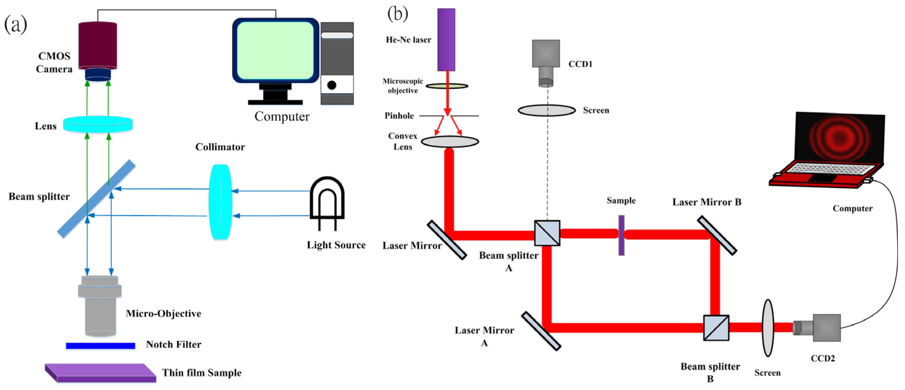
Figure 1a shows a schematic diagram of the measurement system used to evaluate image contrast. The working distance was 30 mm and the actual size of the test sample was 25 mm in diameter. A light source formed a parallel beam through a collimator. The beam splitter divided the light into two parallel beams, one of which was directed towards the test sample through a microscope objective and a notch filter. The light reflected by the test sample returned through the beam splitter and was directed to the CMOS camera, where an image was formed and displayed on a computer monitor.
A Mach–Zehnder interferometer was used to measure the residual stress in the thin films, as shown in
Figure 1b. The measuring system used a helium-neon laser (Melles Griot, Artisan Technology Group, Champaign, IL, USA) with a wavelength of 632.8 nm as the light source. The spatial filter was used to form a point light source, and then a uniform parallel beam was generated through a collimating lens. The incident beam was divided into two beams after passing through the first beam splitter. The beams passing through the second beam splitter were finally recombined into a single beam, which was imaged on a ground glass screen and formed an interference fringe. The CCD camera was used to capture the interference pattern, and the computer analyzed the image captured by the CCD camera. We developed a MATLAB program to process all interferograms. The surface profile of the optical thin film could be reconstructed using the fast Fourier transform method [
19] and the phase-unwrapped method [
20]. The radius of curvature of the thin-film samples could be determined with the curve fitting method. The residual stress in thin films is related to the change in the radius of curvature before and after film deposition. The residual stress value in thin films can be determined using the modified Stoney’s formula [
21,
22].
where σ is the residual stress in the thin film,
νs is the Poisson’s ratio for the substrate,
Es is the Young’s modulus for the substrate,
tf is the thickness of the film,
ts is the thickness of the substrate, and
R1 and
R2 represent the radius of curvature of the substrate before and after coating.
The fabricated notch filters were also subjected to microstructural inspection. The root-mean-square (RMS) surface roughness of the notch filters was measured with a Linnik microscopic interferometer, which has been described in previous publications [
23,
24]. In the Linnik microscopic interferometer, one beam is directed onto a test surface through a cube beam-splitter and a microscope objective (20×), while another beam is reflected by a reference mirror (flatness λ/20) and a cube beam-splitter. The resulting interference fringe pattern is recorded by a CCD camera. For the measurement range, 240 × 240 pixels can be chosen for analysis, indicating that the actual size is 100 × 100 μm.
Atomic force microscopy (AFM) is a powerful tool for measuring surface roughness at the nanometer scale. The tip of the atomic force microscope scans over the sample’s surface to measure the topography. The tip interacts with the sample surface, and the forces between the tip and sample are recorded to create a topographic image of the sample’s surface. The root-mean-square (RMS) roughness of thin films can be calculated by averaging the deviations in height from the mean surface height squared over the scanned area. This gives a measure of the average height variations on the sample surface. Scanning electron microscope (SEM) works by scanning a beam of high-energy electrons over the surface of a sample, which causes the electrons to interact with the atoms on the surface and produce signals that can be detected to create an image of the sample. In addition, the surface microstructure and cross-sectional images of the multilayer thin-film filters were observed using a cold-field emission scanning electron microscope (model: Hitachi FESEM S-4800, Tokyo, Japan). SEM can provide information about the topography and composition of thin films, as well as their morphology, crystal structure, and defects. SEM can also be used to analyze the thickness and uniformity of a thin film by measuring the intensity of the signals produced.
4. Conclusions
In this study, two single-wavelength notch filters and one dual-wavelength notch filter (620 and 480 nm) were prepared using an electron-beam evaporation with IAD technique. For the optical properties, the transmittances of the notch filters at the center wavelengths of 480 and 620 nm with normal incidence were 17.5% and 18.5%, respectively. The results from the microscope observation significantly improved the clarity and contrast of the thin-film image. We added 620 and 480 nm notch filters in front of the thin film sample with an optical microscope to obtain higher contrast images. For the residual stress in the notch filter, after depositing a 480 nm notch filter on the back surface of the 620 nm notch filter, the residual stress decreased from −256 to 10.8 MPa. The surface contour of the substrate changed from convex to concave, indicating a transition from compressive stress to small tensile stress. The residual stress in the dual-band (wavelengths of 480 and 620 nm) notch filter could be reduced using a double-sided coating technique. The residual stress in the dual-band notch filter was much lower than that in the single-wavelength notch filters, which is beneficial for machine vision applications and reliable durability. In the surface roughness measurements, the RMS surface roughness was measured by AFM, which showed values of 2.216 for the 480 nm notch filter and 1.807 for the 620 nm notch filter. This indicated that it had low scattering loss characteristics and could maintain high transmittance in the passband. In the FE-SEM microscopic image, it can be seen that the particles on the surface of the notch filter were fine and smooth. In the side view of the structure, the structure of the SiO2 film was mostly continuous and dense, while the Ta2O5 film was observed as a columnar structure. Using the proposed notch filters, the results observed with an optical microscope significantly improved the clarity and image contrast. The results also indicated that the optical properties of the dual-band notch filter were superior to those of single-wavelength notch filters, improving the contrast of the image observation. In summary, the proposed optical notch filters can provide rich and saturated colors with good stability while also providing durable, low-residual-stress performance in terms of mechanical properties. They have potential applications in machine vision, biological imaging, and dynamic monitoring.


