
The Influence of Bias Voltage and Gas Pressure on Edge Covering during the Arc-PVD Deposition of Hard Coatings

Abstract
:1. Introduction
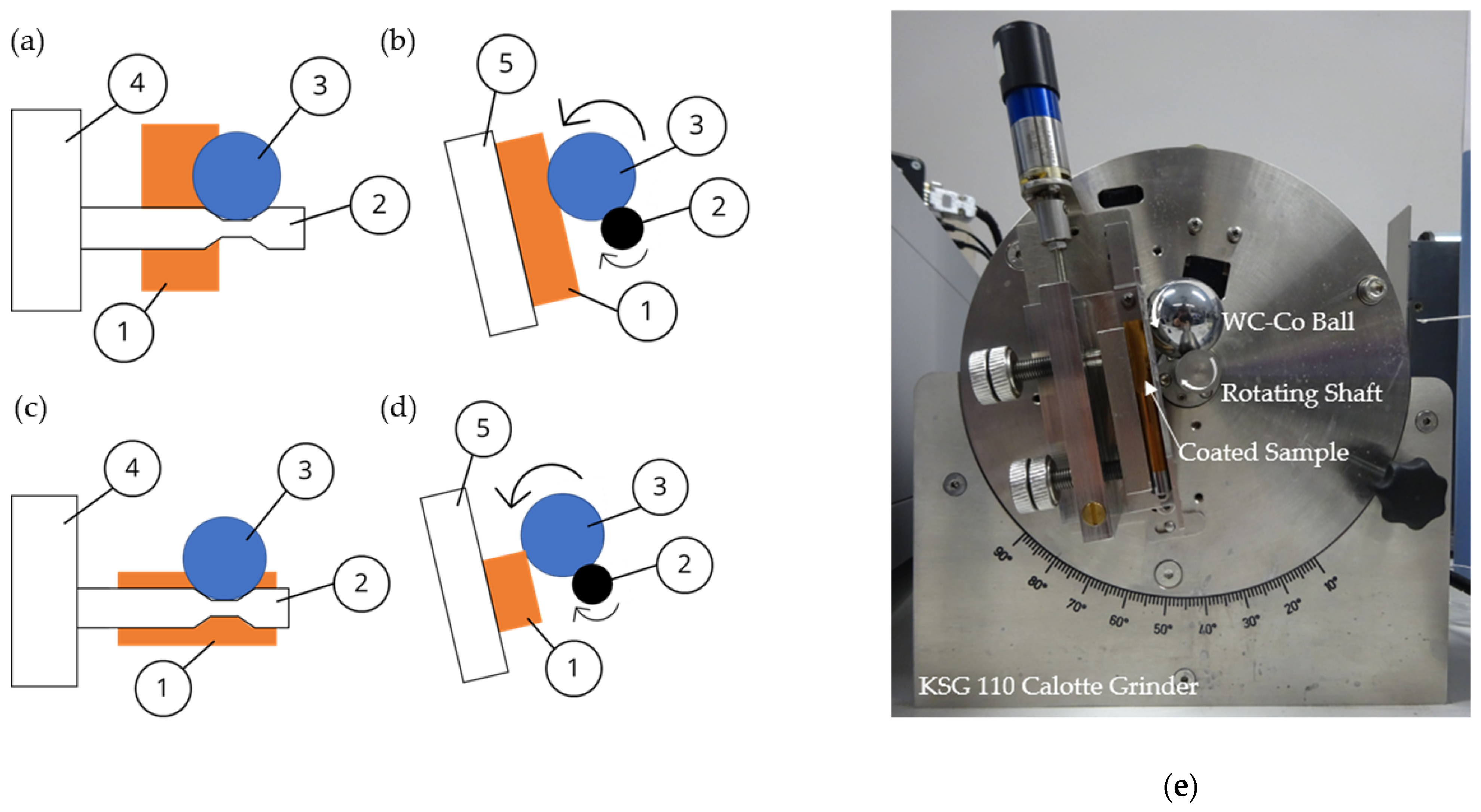
2. Materials and Methods
3. Results
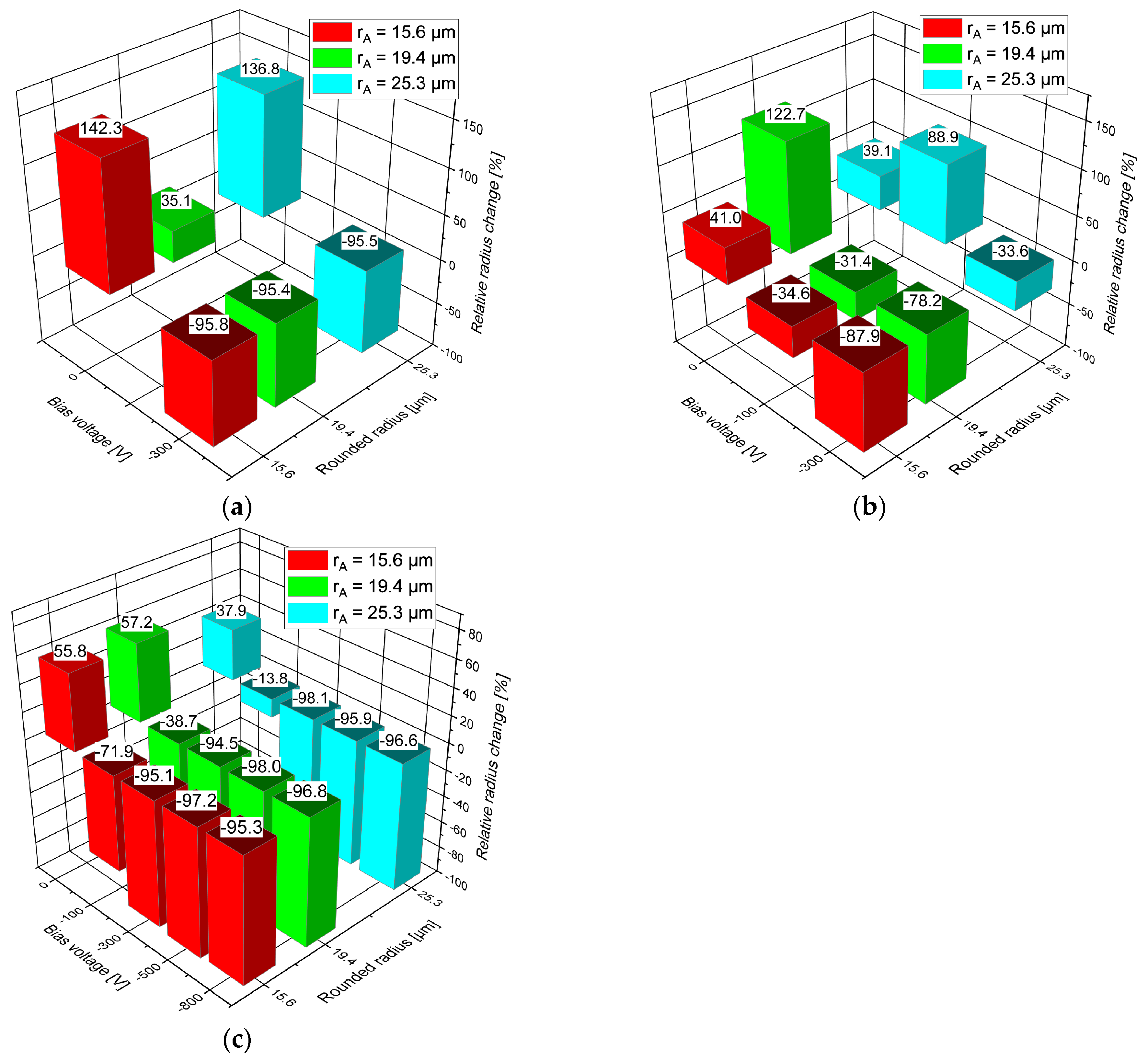
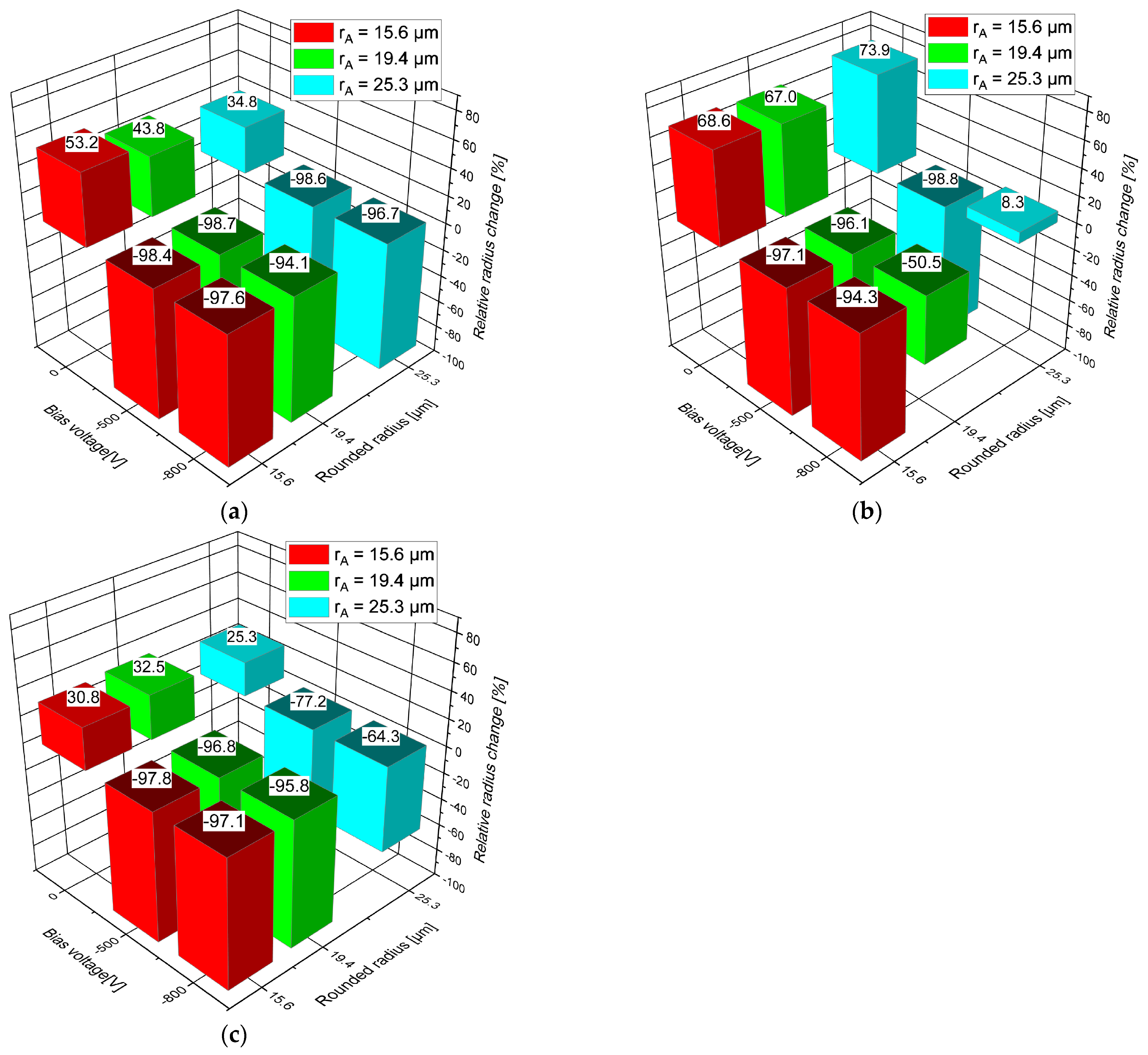
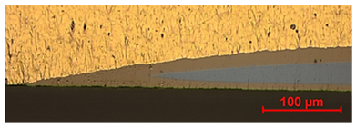
3.1. Application of Coating Material to the Edges
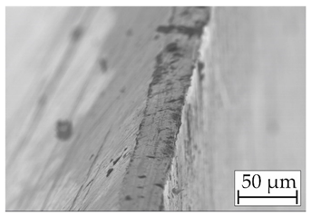
3.2. Layer Properties in Edge Area
3.3. Pressure Variation
3.4. Stability Testing of the Edges
4. Summary and Conclusions
Author Contributions
Funding
Institutional Review Board Statement
Informed Consent Statement
Data Availability Statement
Acknowledgments
Conflicts of Interest
References
- Dobrzanski, L.; Polok, M.; Panjan, P.; Bugliosi, S.; Adamiak, M. Improvement of wear resistance of hot work steels by PVD coatings deposition. J. Mater. Process. Technol. 2004, 155–156, 1995–2001. [Google Scholar] [CrossRef]
- Gold, P.; Loos, J. Wear resistance of PVD-coatings in roller bearings. Wear 2002, 253, 465–472. [Google Scholar] [CrossRef]
- Inspektor, A.; Salvador, P.A. Architecture of PVD coatings for metalcutting applications: A review. Surf. Coat. Technol. 2014, 257, 138–153. [Google Scholar] [CrossRef]
- Jehn, H.A.; Rother, B.; Kappl, H.; Ebersbach, G. PVD coating of 3D parts studied with model samples. Surf. Coat. Technol. 1997, 94–95, 232–236. [Google Scholar] [CrossRef]
- Watterson, P. Child-Langmuir sheath structure around wedge-shaped cathodes. J. Phys. D Appl. Phys. 1989, 22, 1300–1307. [Google Scholar] [CrossRef]
- Schneidkantenpräparation. Ziele, Verfahren und Messmethoden, 1st ed.; Tikal, F., Ed.; University Kassel Press: Kassel, Germany, 2009; ISBN 978-3-89958-494-3. [Google Scholar]
- Denkena, B.; Biermann, D. Cutting edge geometries. CIRP Ann. Manuf. Technol. 2014, 63, 631–653. [Google Scholar] [CrossRef]
- Johansson, B.O.; Sundgren, J.-E.; Hentzell, H.; Karlsson, S.-E. Influence of substrate shape on TiN films prepared by reactive sputtering. Thin Solid Film. 1984, 111, 313–322. [Google Scholar] [CrossRef]
- Rother, B.; Kappl, H.; Pfeifer-Schäller, I.; Jehn, H.A. Characterization of TiN-coated high speed steel cutting edges by load-indentation measurements. Surf. Coat. Technol. 1996, 79, 225–230. [Google Scholar] [CrossRef]
- Rother, B.; Kappl, H.; Pfeifer-Schäller, I.; Ebersbach, G.; Jehn, H. Property distribution on three-dimensionally shaped PVD-coated samples. Surf. Coat. Technol. 1997, 97, 200–203. [Google Scholar] [CrossRef]
- Kim, S.S.; Han, J.G.; Lee, S.Y. Deposition behaviours of CrN films on the edge area by cathodic arc plasma deposition process. Thin Solid Film. 1998, 334, 133–139. [Google Scholar] [CrossRef]
- Novák, R.; Kvasnička, I.; Nováková, D.; Malá, Z. Study of hard PVD coatings on strongly curved surfaces. Surf. Coat. Technol. 1999, 114, 65–69. [Google Scholar] [CrossRef]
- Macak, E.B.; Münz, W.-D.; Rodenburg, J.M. Electron microscopy studies of hard coatings deposited on sharp edges by combined cathodic arc/unbalanced magnetron PVD. Surf. Coat. Technol. 2002, 151–152, 349–354. [Google Scholar] [CrossRef]
- Macak, E.B.; Münz, W.-D.; Rodenburg, J.M. Edge Related Effects During Ion Assisted PVD on Sharp Edges and Implications for Coating of Cutting Tools. Surf. Eng. 2003, 19, 310–314. [Google Scholar] [CrossRef]
- Macak, E.; Münz, W.; Rodenburg, J. Plasma–surface interaction at sharp edges and corners during ion-assisted physical vapor deposition. Part I: Edge-related effects and their influence on coating morphology and composition. J. Appl. Phys. 2003, 94, 2829–2836. [Google Scholar] [CrossRef]
- Macak, E.; Münz, W.; Rodenburg, J. Plasma–surface interaction at sharp edges and corners during ion-assisted physical vapor deposition. Part II: Enhancement of the edge-related effects at sharp corners. J. Appl. Phys. 2003, 94, 2837–2844. [Google Scholar] [CrossRef]
- Flöter, A.; Gluche, P. Verbesserung der Schärfe diamantbeschichteter Hartmetallklingen. Ind. Diam. Rundsch. IDR 2004, 38, 110–112. [Google Scholar]
- Qin, F.; Chou, Y.K.; Nolen, D.; Thompson, R.G. Coating thickness effects on diamond coated cutting tools. Surf. Coat. Technol. 2009, 204, 1056–1060. [Google Scholar] [CrossRef]
- Sato, Y.; Kawamura, J.; Nagase, T.; Pahlovy, S.A.; Miyamoto, I. Sharpening of CVD diamond coated tools by 0.5–10 keV Ar+ ion beam. Diam. Relat. Mater. 2011, 20, 954–959. [Google Scholar] [CrossRef]
- Bohlmark, J.; Blomqvist, H.; Landälv, L.; Amerioun, S.; Ahlgren, M. Evaluation of arc evaporated coatings on rounded surfaces and sharp edges. Mater. Sci. Forum 2011, 681, 145–150. [Google Scholar] [CrossRef]
- Krülle, T.; Kaulfuß, F.; Zimmer, O.; Leyens, C. Nano-Design für Makroschichten. Vak. Forsch. und Prax. 2018, 30, 46–49. [Google Scholar] [CrossRef]
- Krülle, T.; Kaulfuß, F.; Zimmer, O.; Leyens, C. Neue Ansätze zur Beschichtung von Werkzeugkanten. In Jahrbuch Oberflächentechnik 2019, 1st ed.; Sörgel, T., Ed.; Eugen G. Leuze Verlag: Bad Saulgau, Germany, 2019; pp. 65–77. ISBN 978-3-87480-357-1. [Google Scholar]
- Bouzakis, K.; Michailidis, N.; Skordaris, G.; Kombogiannis, S.; Hadjiyiannis, S.; Efstathiou, K.; Pavlidou, E.; Erkens, G.; Rambadt, S.; Wirth, I. Optimisation of the cutting edge roundness and its manufacturing procedures of cemented carbide inserts, to improve their milling performance after a PVD coating deposition. Surf. Coat. Technol. 2003, 163–164, 625–630. [Google Scholar] [CrossRef]
- Han, H.; Lee, N. Sputter deposition modeling of Ti thin film on a sharp tip. Thin Solid Film. 2005, 475, 144–149. [Google Scholar] [CrossRef]
- Vereshchaka, A.A.; Vereshchaka, A.S.; Mgaloblishvili, O.; Morgan, M.N.; Batako, A.D. Nano-scale multilayered-composite coatings for the cutting tools. Int. J. Adv. Manuf. Technol. 2014, 72, 303–317. [Google Scholar] [CrossRef]
- Meindlhumer, M.; Jäger, N.; Spor, S.; Rosenthal, M.; Keckes, J.F.; Hruby, H.; Mitterer, C.; Daniel, R.; Keckes, J.; Todt, J. Nanoscale residual stress and microstructure gradients across the cutting edge area of a TiN coating on WC Co. Scr. Mater. 2020, 182, 11–15. [Google Scholar] [CrossRef]
- Čekada, M.; Panjan, P.; Drnovšek, A.; Drobnič, M. Increase of coating thickness on sharp edges, deposited by cathodic arc evaporation. Surf. Coat. Technol. 2021, 405, 126691. [Google Scholar] [CrossRef]
- DIN EN ISO 26423:2016-11; Hochleistungskeramik—Bestimmung der Schichtdicke mit dem Kalottenschleifverfahren. Beuth Verlag GmbH: Berlin, Germany, 2016; ICS 81.060.30 (DIN EN ISO 26423).
- Litterst, T.; Krülle, T.; Zimmer, O. Einstellung der Kantenschärfung durch kontrolliertes Wachstum von nitridischen Hartstoffschichten an Schneidkanten und deren Charakterisierung. In Jahrbuch Oberflächentechnik 2022, 1st ed.; Sörgel, T., Ed.; Eugen G. Leuze Verlag KG: Bad Saulgau, Germany, 2022; ISBN 978-3-87480-380-9. [Google Scholar]


| Coating Material | Deposition Process | Main Results | References |
|---|---|---|---|
| TiN | RMS | There was a TiN layer thickness variation at different bias potentials: between −350 and −500 V, no coating could be deposited on the sample edges, while at a lower bias potential of −200 V, TiN coatings could be deposited. Even thicker layers could be achieved at bias potentials between −32 and −150 V, due to lower back sputtering. Increasing the Ar gas pressure weakened the edge effect; the back sputtering was suppressed; and the coating thickness increased. | [8] |
| TiN | MS | There was a determination of geometry-dependent hardness curves. Denser and harder layers were formed near the edges. A larger edge angle yielded a harder deposited layer. | [9] |
| TiN | DMS + UBMS | There was a determination of the geometry-dependent layer thickness distribution. Sharper edges yielded a lower layer thickness; the hardness increased towards the edge; and a sharper edge yielded a lower hardness. | [10] |
| TiN | RMS, CAE, HCD | The coating thickness on the edges decreased due to back sputtering, and the coating thickness decreased with a decreasing wedge angle. With CAE coating, there was a better depth coatability due to higher ionization of the plasma; a higher gas pressure led to a higher coating thickness at the edge; the hardness at the edges was lower than on the flat specimen. Furthermore, an analysis of the coatability of edges with edge angles of 30°, 54°, and 90°, as well as the recesses, was carried out. Compared to other coating processes, CAE provided the highest coating rates, as well as a relatively uniform coating thickness distribution along the edges. At an edge angle of 30°, the coating thickness decreased with the increasing distance from the edge, while at 54° and 90°, the coating thickness initially decreased but increased again with an increasing distance from the edge. When determining the coating hardness, it was found that coatings produced with CAE have a higher coating hardness than coatings deposited by RMS. | [4] |
| CrN | CAE | The performance of coatings on samples with different edge angles and a flat sample was considered. When applying a bias voltage, an increased accumulation of macro particles and thus a roughening of the edge was observed with a decreasing edge angle and an increasing voltage between −100 V and −400 V. In addition, an increase in the coating rate with an increasing edge angle was observed in the edge region compared to a flat sample. The accumulation of macro particles could be reduced by a pulsed bias voltage. | [11] |
| TiN | CAE, RMS | Two geometries (cutting edges with right-angled and acute-angled edges) were coated at bias voltages of 0 V, −30 V, and −60 V. As the bias voltage increased, the coating rate decreased and the residual compressive stresses increased. During the bias voltage coating process, increased ion bombardment occurred at the edges and tips of the curved samples. | [12] |
| TiAlCrYN, TiAlN/VN, | CAE + UBMS | Coatings deposited on the edges under increased ion flux density showed different properties than coatings on flat substrates. For this purpose, a comparative study of TiAlCrYN layers on different samples (angles of 30°, 45°, and 60° and radii of 2 µm and 100 µm) was carried out. The applied bias voltage was −75 V. The Al/Ti ratio increased slightly with increasing distance from the edge and an increasing edge angle, indicating partial back sputtering back Al at the edge. While the Al/Ti ratio was almost the same for all samples at the edge, it diverged with an increasing distance from the edge. For the 60° edge, the Al/Ti ratio reached the value of the flat sample with an increasing edge distance. The influence of the edge radius was more pronounced for the 30° edge than for the 60° edge. Smaller radius yielded a smaller Al/Ti ratio, due to the stronger sputtering effect. All edges had a thicker layer compared to the flat samples, with the effect decreasing with an increasing edge angle. This was in contrast to the investigations of TiAlN/VN coatings. The coatings were deposited at −75 V to −150 V. An influence of the edge (angles of 30°, 45°, and 90°) on the angle of incidence of the ions was found, resulting in changes of the morphology, thickness, composition, and structure of the layers. Directly at the edge (up to 0.3 mm), the layer was completely absent; and in the area near the edge (1–2 mm from the edge), the layer started to partially delaminate, which was accompanied by a decrease in the Al/Ti ratio and an increase in the ion incidence angle and ion flux density. Undisturbed regions far from the edge were characterized by a dense layer, a constant Al/Ti ratio, a constant back sputtering rate of Al, a constant ion flux density, and an ion incidence angle of 0°. Directly at the edge, the Al back sputter rate was an order of magnitude higher than in the undisturbed region far from the edge, and the incidence angle increased from 0° to almost 90°. In addition, there was a strong increase in the ion flux density. The following influencing variables were observed. The edge effects were related to the shape of the plasma boundary layer, which was influenced by the edge geometry. The re-sputtering rate depended on the energy of the ion flux (bias-dependent) and the type of ions (Ar ions lead to a higher sputtering yield than N ions). In summary, a zone diagram was developed which describes the relationship between the bias voltage and edge angle. There was a division into three zones: Zone 1:, where the edges have a homogeneous and closed layer even away from the edge; Zone 2. Where the layer along the edge is partially missing; and Zone 3, where the layer along the edges is completely missing. | [13,14,15,16] |
| Diamond | CVD | There was the development of a plasma sharpening process with Ar ions for edge sharpening. The cutting edge became sharper than the initial tool. | [17,18,19] |
| TiAlCrSiN, TiAlN | CAE | Re-sputtering on the edges led to a sharpening effect, as the sputtering yield increased. A bias voltage of −80 V led to a slight sharpening of the edge and a high residual stress; a bias voltage of −40 V, on the other hand, led to less wear during machining. | [20] |
| AlCrSiN/TiN | CAE | This was an investigation of the influence of the bias voltage and the initial edge geometry on the edge radius and the sharpening of the cutting edge during coating. The wedge angle changed only slightly due to the coating. | [21,22] |
| TiAlN | Simulation, PVD | The fatigue and wear behavior of coated inserts with different cutting radii was investigated experimentally. The inserts with cutting radii from 8 µm to 35 µm were manufactured by honing and microblasting. It was found that the wear behavior of the cutting radii produced by honing was significantly improved compared to those produced by microblasting. In addition, an increase in the cutting radius resulted in an increase in the tool life. | [23] |
| Ti | Simulation, PVD | The deposition behavior of Ti films on a sharp tip was investigated by simulation for conventional and ionized PVD coatings. In conventional PVD, it was found that the morphology at the sharp tip was difficult to control, because the energy and flux of the sputtered particles could not be properly controlled. With ionized PVD, the morphology at the tip could be controlled. It was found that with a smaller edge angle, the deposition rate was lower but the uniformity of the layer was improved. | [24] |
| TiAlN based multi layers | FCVAD | There as the development of an approach for the design of multilayer composite coatings on a nanoscale for cutting tools. Various analyses were carried out to map the effects of the developed composite coatings on tool wear rates. | [25] |
| TiN | CAE | This was a characterization of the stress state in the edge area of a coated cutting tool made of a WC-Co carbide. The coating was carried out at a bias voltage of −100 V and a coating pressure of 4 Pa. At the flank face, an increase in compressive stress from the substrate surface to the coating surface from −1.2 GPa to −2.5 GPa could be seen, which was due to the development of microstructures during the coating process. At the cutting edge directly, the residual stresses were low but increased to −3 GPa towards the outer surface. The maximum coating thickness was also found in this area. At the rake face, scattering stresses of up to −3 GPa were observed. A hypothesis for this effect was a nanoporous microstructure. | [26] |
| TiAlN | CAE | This was an investigation of layer growth on sharp tool edges. The layer thickness was constant over most of the free surfaces but increased significantly on all analyzed edges (by a factor of 1.5 to 1.8). The increase in the layer thickness was successive and not abrupt. In the area where the two edges met, the effect of the layer thickness increase multiplied. | [27] |
| Cathode Material | Cathode Dimension [mm] | Cathode Composition [at. %] |
|---|---|---|
| Ti | 440 × 170 × 20 | 100 |
| AlCrSi | Ø105 × 15 | 66/29/5 |
| AlTi | Ø63 × 420 | 50/50 |
| AlTi | Ø105 × 15 | 66/34 |
| AlTi | Ø105 × 15 | 70/30 |
| AlTi | Ø63 × 420 | 80/20 |
| Cr | Ø63 × 420 | 100 |
| Ti | Ø105 × 15 | 100 |
| Nominal Initial Radii ry | Measured Initial Radii rA |
|---|---|
| ry = 10 µm | rA,10µm = (15.6 ± 1.9) µm |
| ry = 15 µm | rA,15µm = (19.4 ± 4.1) µm |
| ry = 20 µm | rA,20µm = (25.3 ± 2.2) µm |
| UB = 0 V | UB = −800 V |
|---|---|
 | |
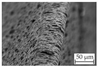
| Uncoated substrate (cutting blade) | |
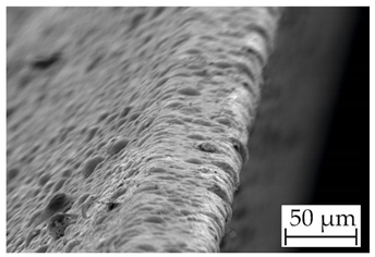 | 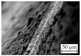 |
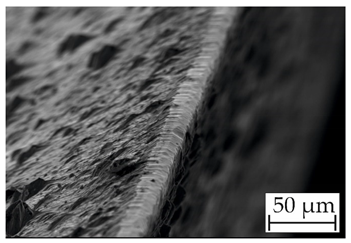
| TiN-coated cutting blades | |
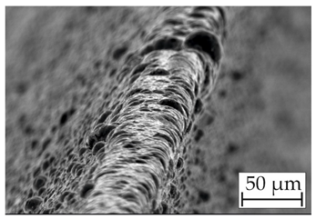 |  |
| AlTiN-coated cutting blades | |
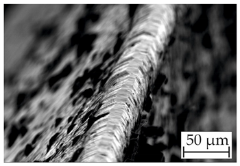
 |  |
| AlTiN/TiN-coated cutting blades | |
| Coating Adhesion (Zone 1) | Coating Defects (Zone 2) | Coating-Free Edge (Zone 3) |
|---|---|---|
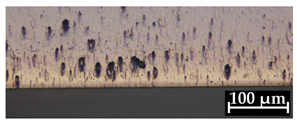 |  |  |
| AlTiN(70/30)/TiN; p = 5 Pa; and UB = −500 V | AlTiN(70/30)/TiN; p = 5 Pa; and UB = −300 V | TiN; p = 1 Pa; and UB = −500 V |
| Coating System | N2 Pressure [Pa] | UB = 0 | UB = −100 V | UB = −300 V | UB = −500 V | UB = −800 V |
|---|---|---|---|---|---|---|
| TiN | 1 | coating adhesion | defects | coating adhesion | free edge | free edge |
| 2 | coating adhesion | coating adhesion | coating adhesion | free edge | free edge | |
| 5 | coating adhesion | coating adhesion | coating adhesion | coating adhesion | coating adhesion | |
| AlTiN | 1 | coating adhesion | defects | defects | coating adhesion | no coating |
| 2 | coating adhesion | defects | defects | coating adhesion | coating adhesion | |
| 5 | coating adhesion | defects | defects | coating adhesion | coating adhesion | |
| AlTiN/TiN | 1 | coating adhesion | defects | defects | coating adhesion | coating adhesion |
| 2 | coating adhesion | defects | defects | coating adhesion | coating adhesion | |
| 5 | coating adhesion | defects | defects | coating adhesion | coating adhesion |
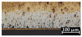
| Layer Adhesion | Layer Delamination |
|---|---|
 TiN, UB = −500 V, and transverse grinding |  AlTiN/TiN, UB = −500 V, and longitudinal grinding |
| UB = 0 | UB = −500 V | UB = −800 V | |
|---|---|---|---|
| TiN | coating adhesion | coating adhesion | coating adhesion |
| AlTiN | coating adhesion | delamination | coating adhesion |
| AlTiN/TiN | coating adhesion | delamination | coating adhesion |
| UB = 0 | UB = −500 V | UB = −800 V | |
|---|---|---|---|
| TiN | coating adhesion | coating adhesion | coating adhesion |
| AlTiN | delamination | delamination | coating adhesion |
| AlTiN/TiN | coating adhesion | delamination | coating adhesion |
| rA = 15.6 µm | rA = 19.4 µm | |
|---|---|---|
| AlTiN UB = −500 V | 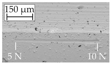 | 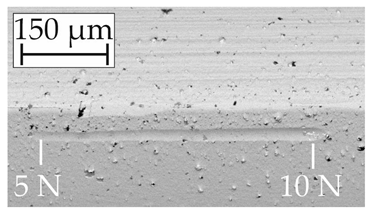 |
| AlTiN UB = −800 V | 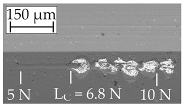 | 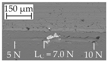 |
| AlTiN/TiN UB = −500 V |  |  |
| AlTiN/TiN UB = −800 V |  | 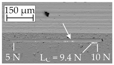 |
Disclaimer/Publisher’s Note: The statements, opinions and data contained in all publications are solely those of the individual author(s) and contributor(s) and not of MDPI and/or the editor(s). MDPI and/or the editor(s) disclaim responsibility for any injury to people or property resulting from any ideas, methods, instructions or products referred to in the content. |
© 2024 by the authors. Licensee MDPI, Basel, Switzerland. This article is an open access article distributed under the terms and conditions of the Creative Commons Attribution (CC BY) license (https://creativecommons.org/licenses/by/4.0/).
Share and Cite
Zimmer, O.; Krülle, T.; Litterst, T. The Influence of Bias Voltage and Gas Pressure on Edge Covering during the Arc-PVD Deposition of Hard Coatings. Coatings 2024, 14, 732. https://doi.org/10.3390/coatings14060732
Zimmer O, Krülle T, Litterst T. The Influence of Bias Voltage and Gas Pressure on Edge Covering during the Arc-PVD Deposition of Hard Coatings. Coatings. 2024; 14(6):732. https://doi.org/10.3390/coatings14060732
Chicago/Turabian StyleZimmer, Otmar, Tim Krülle, and Thomas Litterst. 2024. "The Influence of Bias Voltage and Gas Pressure on Edge Covering during the Arc-PVD Deposition of Hard Coatings" Coatings 14, no. 6: 732. https://doi.org/10.3390/coatings14060732