Article

Enhancing Photovoltaic Performance and Stability of Perovskite Solar Cells through Single-Source Evaporation and CsPbBr3 Quantum Dots Incorporation

School of Intelligent Manufacturing, Longdong University, Qingyang 745000, China
*
Authors to whom correspondence should be addressed.
Coatings 2023, 13(5), 863; https://doi.org/10.3390/coatings13050863
Submission received: 9 April 2023 / Revised: 27 April 2023 / Accepted: 28 April 2023 / Published: 1 May 2023

Abstract

:
This study investigates the potential of inorganic perovskite CsPbBr3 as a photovoltaic material, highlighting its superior stability compared to that of organic–inorganic hybrid perovskite materials. Conventional methods for preparing CsPbBr3 perovskite films, such as the two-step method and the dual-source thermal evaporation method, face challenges in obtaining high-purity films due to the decomposition of precursor films and the formation of multiple heterogeneous phases. To address this issue, we synthesized CsPbBr3 powder material using thermal evaporation deposition, which effectively suppressed decomposition and the formation of heterogeneous phases. Consequently, we achieved uniform and dense CsPbBr3 perovskite films. By incorporating energy-band engineering modification with CsPbBr3 quantum dots (QDs), the all-inorganic perovskite solar cells (PSCs) attained a power conversion efficiency (PCE) of 7.01% under standard solar illumination conditions. The device PCE remained at 93% of its initial efficiency under 30% relative humidity conditions for over 100 days, showcasing its durability. The developed method produced an average grain size of 800 nm, resulting in a smooth and uniform film surface, thereby demonstrating the method’s high repeatability. Additionally, the optimized PSCs exhibited a high open-circuit voltage (VOC) with the champion device reaching a VOC of 1.38 V and a PCE of 7.01%. This research presents a robust, efficient, and cost-effective approach for fabricating high-quality all-inorganic PSCs.

1. Introduction

Organic–inorganic hybrid perovskite solar cells (PSCs) have experienced remarkable advancements from 2009 to 2023, demonstrating immense potential for commercial and military applications [1,2,3,4,5,6]. The champion power conversion efficiency (PCE) in PSCs has reached as high as 25.7% by optimizing perovskite film properties and charge transfer capacity [7,8,9,10,11,12,13]. However, hybrid organic–inorganic PSCs still suffer from limited stability due to the inherent instability of hybrid perovskite materials in air conditions (oxygen-rich, moisture, heat, and light) [14,15], hindering further development. Therefore, exploring high-stability photovoltaic materials and designing novel device structures are crucial for promoting future applications and commercialization. To circumvent the instability of organic–inorganic hybrid perovskite materials, researchers have focused on stable all-inorganic halide perovskites of the type CsPbX3 (X = I, Br, Cl, or mixed halides) for use in PSCs to enhance their stability. All-inorganic materials, including CsPbI3 [16], CsPbI2Br [17], CsPbIBr2 [18], and CsPbBr3 [19], have been extensively studied due to their outstanding optical performance and enhanced stability [20,21,22]. Among these inorganic materials, CsPbBr3 exhibits the best stability, providing protection against heat and moisture [23]. Kumar and colleagues demonstrated that CsPbBr3 quantum dots are especially promising for improving the performance of photovoltaic devices due to their size-dependent energy gaps, high photoluminescence quantum yields, and advantageous band alignments [24].
Developing an efficient method for preparing inorganic CsPbBr3 perovskite films is essential for achieving high film quality and device performance. Historically, solution processes have been employed to fabricate most CsPbBr3 PSCs [25,26,27]. Nonetheless, CsPbBr3 films prepared via solution engineering still exhibit minor degradation under UV irradiation. The solution process likely contributes to the imperfect photostability of CsPbBr3 and results in high concentrations and low resistance to ultraviolet rays. Although solution-based processes do not require expensive vacuum equipment, they struggle to produce consistent, large-area, high-quality CsPbBr3 films. Vacuum thermal evaporation (VTE), a mature technique commonly used in the coating industry, offers the ability to deposit multiple thin films on large areas, yielding excellent uniformity and flatness. However, VTE has been relatively underexplored for fabricating PSCs, especially compared to solution processes. Ma et al. utilized dual-source vacuum thermal evaporation to fabricate high-efficiency PSCs [28], demonstrating that vapor-deposited films can achieve uniformity. More recently, Chen et al. employed two-source VTE to fabricate high-performance CsPbBr3-based organic solar cells with efficiencies of 14.03% [29]. Dual-source VTE has also been applied to fabricate other PSCs [30,31,32,33,34,35]. Bolink et al. successfully used MAI, CsBr, FAI, and PbI2 as evaporation sources to prepare triple-cation Cs0.5FA0.4MA0.1Pb(I0.83Br0.17)3 perovskite films and manufacture solar cells with an efficiency of 16% [36].
In multi-source thermal evaporation, the raw material evaporation rate ratio significantly impacts the deposited film stoichiometry and PSC efficiency. Factors such as vacuum chamber pressure, crucible heating power, and the amount and distribution of evaporated material in the crucible all influence the evaporation rate ratio. Maintaining the correct evaporation rate of raw material throughout the process is challenging due to constantly changing experimental conditions, and adjusting and controlling the ratio of raw material evaporation rate is both difficult and time-consuming.
In this study, we employed a single crucible, single-source VTE method to deposit high-quality CsPbBr3 thin films, which proved to be a simple and effective approach. We synthesized high-purity CsPbBr3 material powder, compressed it into tablets, and placed it in a quartz crucible. The synthesis of CsPbBr3 powder in our study was adapted from the method reported by Zhang et al. [37], with some modifications to optimize the process for our experimental setup. Zhang and colleagues have demonstrated a facile and efficient approach for the synthesis of highly luminescent CsPbBr3 perovskite powder. We investigated the effects of evaporation rate and CsPbBr3 film thickness on film quality and solar cell performance. Furthermore, we spin-coated a layer of quantum dots (QDs) on the TiO2 electron transport layer to optimize energy level matching, thereby enhancing electron extraction capability and PCE [38]. Through continuous optimization, we successfully synthesized CsPbBr3 thin films and fabricated a stable CsPbBr3 solar cell with an efficiency of 7.01%. We achieved a PCE of 7.01% using the single-source thermal evaporation method. It is worth noting that some previous studies have reported higher PCE values for CsPbBr3 perovskite solar cells. For example, Zhang et al. reported a PCE of 10.97%. Despite these higher PCE values, our method offers several advantages in terms of simplicity, reproducibility, and uniformity of the CsPbBr3 films [39].

2. Experiment Section

2.1. Materials Synthesis

Lead bromide (PbBr2), cesium bromide (CsBr), and tetrabutyl titanate were procured from Macklin Company. Spiro-OMeTAD was obtained from Xi’an Polymer Light Technology Corp. All other chemicals were purchased from Sigma-Aldrich. In this study, chemicals were used as received without further purification.
CsPbBr3 powder was synthesized by dissolving 5 mmol of CsBr in 10 mL of an aqueous solution and 5 mmol of PbBr2 in 20 mL of hydrogen bromide (48 wt% in an aqueous solution). The solutions were mixed in a 100 mL brown round-bottom flask and stirred vigorously at 0 °C for 12 h. Subsequently, the mixture was transferred to a 100 mL beaker, and 50 mL of absolute ethanol was added to obtain a yellow precipitate. The yellow precipitate was then subjected to rotary evaporation at a constant temperature of 60 °C for 4 h. The powder was dissolved in an aqueous solution and recrystallized in absolute ethanol three times. The yellow powder was dried at 60 °C in a vacuum drying oven for 12 h.
In accordance with previous reports, the preparation of CsPbBr3 quantum dots (QDs) was facilitated by washing the precipitates with toluene through centrifugation at 9000 rpm for 20 min [40]. This washing process was repeated three times to eliminate as many organic ligands on the surface as possible. Finally, the precipitates were redispersed in ethyl acetate, yielding a stable colloidal solution.

2.2. Device Fabrication

A fluorine-doped tin oxide (FTO) glass substrate was etched using zinc powder and 35% HCl, followed by ultrasonic cleaning in acetone, isopropanol, deionized water, and ethanol for 20 min each. The cleaned substrate was then air-dried. To remove any remaining organic residues on the surface, the FTO substrate was treated with oxygen plasma for 10 min. A dense TiO2 layer was spin-coated using a 0.15 M solution of diisopropoxy titanium bis (acetylpyruvate) (75 wt.% in isopropanol) in 1-butanol at 2000 rpm for 30 s. The coated substrate was then sintered at 500 °C for 30 min.
A 1 mL solution of CsPbBr3 quantum dots (QDs) was spin-coated onto the TiO2 layer at 2000 rpm for 30 s. The CsPbBr3 light absorption layer was deposited on the FTO/TiO2/CsPbBr3 QDs layer by thermally evaporating CsPbBr3 material in a vacuum (Figure 1a). During the thermal deposition process, the deposition chamber was first evacuated to approximately 2 × 10⁻⁵ Pa. The distance between the CsPbBr3 target and the FTO substrate was set at 30 cm. The substrate was then annealed in a nitrogen-protected glove box for 5 min at a temperature of 100 °C.
Subsequently, a Spiro-OMeTAD solution (50 mg of Spiro-MeOTAD, 22.5 μL of 4-tert-butylpyridine, and 22.5 μL of acetonitrile solution containing 170 mg·mL−1 of lithium bis-(trifluoromethylsulfonyl)imide in 1 mL of chlorobenzene) was deposited onto the surface of the CsPbBr3 perovskite layer by spin-coating at 3000 rpm for 35 s in a nitrogen-protected glove box. Finally, gold electrodes with a thickness of 100 nm were deposited by thermal evaporation in a vacuum environment (5 × 10⁻⁴ Pa).

2.3. Device Characterization

Scanning electron microscopy (SEM) was employed to observe the surface morphology of the film and the cross-sectional view of the device. Energy dispersive spectroscopy (EDS) spectra were acquired using a Nova_NanoSEM430 instrument (FEI, Hillsboro, OR, USA). The X-ray diffraction (XRD) pattern of the CsPbBr3 film was obtained using a Rigaku D/max 2550 X-ray diffractometer (Rigaku, Tokyo, Japan) with a monochromatic Cu target radiation source at a scan rate of 4°/min. Atomic force microscopy (AFM, 5500, Agilent, Santa Clara, CA, USA) was utilized to characterize the roughness of CsPbBr3 films. Electrochemical impedance spectroscopy (EIS) measurements were performed using a CHI630E electrochemical analyzer (ChenHua, Shanghai, China). Absorption spectra were recorded using a UV-1800 spectrometer (Shimadzu, Tokyo, Japan). The optical properties of the CsPbBr3 quantum dots and perovskite films were investigated using UV–Vis absorption spectroscopy and photoluminescence (PL) measurements. The absorption spectra were obtained using a UV–Vis spectrophotometer, while the PL spectra were recorded using a spectrofluorometer, following the procedures reported by Kumar et al. [41]. These techniques allowed us to determine the energy gap and emission properties of the CsPbBr3 quantum dots, as well as to evaluate the charge carrier dynamics and recombination processes in the perovskite films. Current–voltage (I−V) measurements under 1-sun conditions (100 mW·cm−2 and AM 1.5 G radiation) were performed using an ABET Sun 2000 solar simulator system, with a Keithley 2400 digital source meter. The light intensity was calibrated using a reference silicon cell (RERA Solutions RR-1002, Shenzhen, China). The incident photocurrent conversion efficiency (IPCE) spectrum was recorded from 400 to 850 nm using a SolarCellScan100 system (ZOLIX, Beijing, China).

3. Results and Discussion

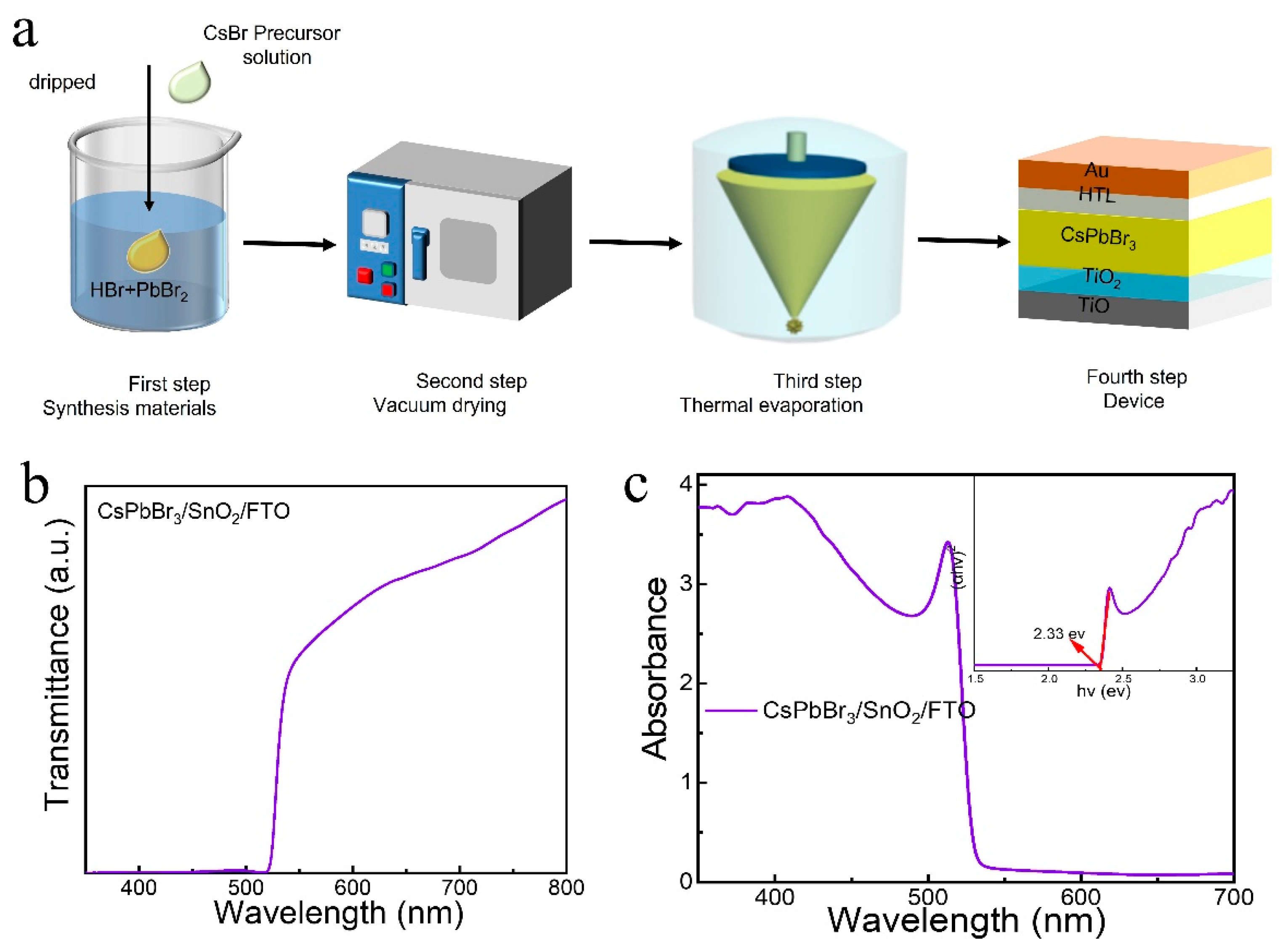
3.1. Structure and Morphology

As illustrated in the preparation Schematic diagrams in Figure 1a, the synthesis process of CsPbBr3 powder involves mixing CsBr in an aqueous solution and PbBr2 in a hydrogen bromide solution at a molar ratio of 1:1, resulting in a yellow-phase CsPbBr3 powder. The yellow powder is then vacuum-dried. The obtained CsPbBr3 powder is deposited onto the TiO2/FTO substrate using vacuum thermal evaporation deposition techniques. The deposited films are yellow in color and exhibit a wide range of uniformity. The CsPbBr3 thin film demonstrates relatively transparent properties with a high average visible light transmittance of 77% in the wavelength range from 550 to 800 nm (Figure 1b) [42]. Additionally, the deposited CsPbBr3 films display strong absorption spectra from 300 to 550 nm in their UV−Vis absorbance spectra, indicating that single-source thermal deposition technology is an effective method for fabricating CsPbBr3 films. The inset in Figure 1c reveals that the optical bandgap of the CsPbBr3 film is 2.33 eV. In addition to the previously reported substrates, we have also prepared CsPbBr3 perovskite films on glass and FTO (fluorine-doped tin oxide) substrates. The preparation procedure was the same as described earlier for the other substrates. The use of glass and FTO substrates allows us to investigate the effect of different substrate materials on the optical and morphological properties of the perovskite films. We have performed UV−Vis absorption spectroscopy and photoluminescence (PL) measurements on the CsPbBr3 perovskite films deposited on both glass and FTO substrates. The absorption and PL spectra of the films on these substrates are presented in Figure 2. The absorption edge and PL peak positions for the CsPbBr3 films on glass and FTO substrates are similar to those observed for the other substrates, indicating that the substrate material has minimal impact on the optical properties of the perovskite films.
As depicted in Figure 3a, the evaporation rate does not alter the cubic phase of CsPbBr3; however, it significantly influences the crystallinity and crystal orientation. Lower evaporation rates result in higher crystallinity and crystal orientation. The morphology of the CsPbBr3 perovskite films plays a crucial role in determining the performance of photovoltaic devices. As observed in Figure 3b, films prepared at lower evaporation rates (0.5 nm/s) exhibit dense and large perovskite grains, which are desirable for high-performance devices. These characteristics reduce the number of grain boundaries where defects are typically located, leading to improved charge transport and minimized charge recombination. On the other hand, films prepared at higher evaporation rates (1.5 or 2 nm/s) display a reduced grain size, which may negatively affect the device performance due to increased grain boundaries and defect sites, The reason behind these observations is that at low evaporation rates, CsPbBr3 molecules have more time to attach to the substrate electrode surface, resulting in a uniform film with large grain size and high orientation. Conversely, high evaporation rates make it difficult for CsPbBr3 molecules to attach to the substrate due to increased kinetic energy, causing coalescence and leading to the formation of cracks, defects, small grains, and low crystallinity in the CsPbBr3 film. This is advantageous for high-performance devices, as dense and large-grained perovskite crystals reduce the boundaries where most defects are located within the grain area [43]. Conversely, when the film is prepared by evaporation at higher rates (1.5 or 2 nm/s), the grain size significantly decreases. CsPbBr3 molecules can more easily attach to the substrate electrode surface at low evaporation rates, ultimately yielding a uniform CsPbBr3 film with large grain size and high orientation. In contrast, a high evaporation rate makes it difficult for CsPbBr3 molecules to attach to the substrate; the increased kinetic energy causes subsequent coalescence, which inevitably leads to cracks and defects in the CsPbBr3 film, accompanied by small grains and low crystallinity [44]. Although slower deposition rates may seem beneficial for improving film quality, there is a limit to the benefits that can be obtained from this approach. Excessively slow deposition rates can lead to increased substrate contamination, formation of unwanted intermediate phases, and an inefficient fabrication process. In our study, we found that a deposition rate of 0.5 nm/s provided an optimal balance between film quality and fabrication efficiency, resulting in the best device performance. The EDS mapping of CsPbBr3 films in Figure 3c confirms the presence and uniform distribution of Cs, Pb, and Br elements, indicating the successful formation of the CsPbBr3 perovskite structure. This uniform elemental distribution is essential for achieving consistent optoelectronic properties across the film and ensuring high performance in photovoltaic devices. The EDS mapping also verifies the stoichiometric composition of the CsPbBr3 perovskite films, which is crucial for maintaining the desired crystal structure and phase purity. Additionally, the SEM images of CsPbBr3 films with different evaporation rates (0.5, 1.5, and 2 nm/s) are shown in Figure 3d1–3. The SEM image and AFM of the CsPbBr3 film evaporated at the lowest rate of 0.5 nm/s exhibit the largest grain size (850 nm) and the smallest roughness (root mean square = 3.17 nm). As the evaporation rate increases, the grain size reduces to 450 nm, further validating the XRD analysis results. In addition, we investigated the effect of different deposition rates on the performance of CsPbBr3 perovskite solar cells. We found that the slow deposition rate yielded the best performance in terms of PCE. The J−V curves for solar cells fabricated at different deposition rates are provided in Table 1, clearly showing the impact of the deposition rate on the device performance.

3.2. Device Performance

Figure 4a displays the device structure of CsPbBr3 PSC, which consists of FTO/TiO2/CsPbBr3 QDs/CsPbBr3/Spiro-OMeTAD/Au layers. In this structure, the CsPbBr3 film serves as the full-inorganic light-absorbing layer, CsPbBr3 QDs are employed to passivate the perovskite and TiO2 contact surfaces, Spiro-OMeTAD is used as the hole transport layer (HTL), and Au electrodes are coated as the anode. To prepare the sample for cross-sectional SEM analysis, we first mechanically cleaved the CsPbBr3 PSC device using a sharp scalpel blade. The device was carefully fractured along the edge, creating a cross-sectional surface that exposed the internal structure of the various layers. The cleaved sample was then mounted on an SEM sample holder using conductive carbon tape, ensuring that the cross-sectional surface was facing upwards. The sample was subsequently coated with a thin layer of gold using a sputter coater to enhance the conductivity and prevent charging effects during SEM imaging. Finally, the cross-sectional SEM image of the CsPbBr3 PSC device was obtained (Figure 4b), illustrating the uniform deposition of each layer. The thicknesses of the CsPbBr3 QDs, TiO2, CsPbBr3, Spiro-OMeTAD, and Au layers are 50, 600, 100, and 100 nm, respectively. Figure 4c presents the energy levels of each functional layer in CsPbBr3-based PSCs, with the energy levels of TiO2, CsPbBr3 QDs, CsPbBr3, Spiro-OMeTAD, and Au obtained from the literature [45]. As illustrated in Figure 4c, the valence and conduction bands of CsPbBr3 QDs align well with those of the hole transport layer (HTL) and the electron transport layer (ETL), respectively. This band alignment enables efficient charge separation and transport across the interfaces: When photons are absorbed by the CsPbBr3 QDs, electron–hole pairs (excitons) are generated. Due to the favorable band alignment, the photogenerated holes can easily transfer to the HTL, while the electrons can efficiently migrate to the ETL. The efficient charge transport minimizes the accumulation of charge carriers at the interfaces, which reduces the likelihood of non-radiative recombination losses. Additionally, the energy levels of the CsPbBr3 QDs help to ensure that the built-in electric field within the device is strong enough to drive charge carriers toward their respective transport layers, further improving charge extraction and reducing recombination losses. The J−V characteristics and relevant parameters, including PCE, are shown in Figure 4d−f, and Table 2 (device parameters for solar cells with various thicknesses) summarizes and compares short-circuit current (JSC), open-circuit voltage (VOC), and fill factor (FF).
The PSCs with a 600 nm film thickness exhibit superior photovoltaic performance compared to other film thicknesses. Notably, the PSC with a 600 nm film thickness demonstrates the highest PCE of 6.52%, with a JSC of 6.15 mA·cm−2, a VOC of 1.35 V, and an FF of 78.53%. This PCE value is 21%, 8%, and 3% higher than the devices with film thicknesses of 400 nm, 500 nm, and 700 nm, respectively. As the CsPbBr3 film thickness increases, PCE, JSC, FF, and VOC show a slight increase, reaching a maximum at a film thickness of 600 nm, followed by a decrease upon further thickness increment. Therefore, the optimal film thickness for PSCs is determined to be 600 nm, at which the PCE improves from 5.37% to 6.52% (Figure 4d). These results suggest that the appropriate thickness can provide both effective light absorption and reduced charge recombination capacities. Although our PCE value might not be the highest among the reported studies, our single-source thermal evaporation method provides a solid foundation for future research to further enhance device performance. The simplicity, reproducibility, and uniformity of our method offer a promising route for synthesizing high-quality CsPbBr3 perovskite films. Future studies could focus on optimizing the perovskite film morphology, thickness, and crystallinity, as well as improving the interfaces between the various layers of the device. Additionally, incorporating passivation techniques to reduce defects and non-radiative recombination could further enhance the PCE of our CsPbBr3 perovskite solar cells.
Based on the aforementioned results, the PSCs were fabricated using a 600 nm thick film. Figure 5a presents the absorption, photoluminescence (PL)/excitation spectra, and SEM images of CsPbBr3 quantum dots (QDs). An excitonic absorption peak at 510 nm and a green emission peak centered at 525 nm are observed for the CsPbBr3 QDs under 365 nm excitation. We can observe that the CsPbBr3 quantum dots exhibit an absorption band edge at approximately 2.3 eV. This value corresponds to the energy gap of the quantum dots, which is a crucial parameter affecting their optical and electronic properties. The energy gap of 2.3 eV indicates that the CsPbBr3 quantum dots absorb light in the visible region of the electromagnetic spectrum, which is consistent with their green emission color. The observed energy gap also plays a significant role in the photovoltaic performance of the perovskite solar cell, as it determines the range of photon energies that can be effectively absorbed and converted into electrical energy by the device. The incorporation of CsPbBr3 quantum dots in our perovskite solar cell contributes to enhanced performance in the UV region. This is due to their size-dependent properties, such as high photoluminescence quantum yields and strong absorption in the UV region, which enable efficient photon harvesting and charge carrier generation. As a result, the presence of CsPbBr3 quantum dots in our device improves the overall efficiency by increasing the photocurrent and power conversion efficiency in the UV region. The J−V curves and PCEs of the CsPbBr3 PSCs with and without QDs are displayed in Figure 5b and Table 2, respectively. The CsPbBr3 PSC with QDs exhibits a higher PCE than the device without QDs, increasing from 6.52% to 7.01%. These results indicate that the QDs enhance the device’s carrier extraction capability. Figure 5c depicts the incident photocurrent conversion efficiency (IPCE) spectra of the CsPbBr3 PSCs over the wavelength range of 350 to 600 nm. The device with QDs demonstrates a higher IPCE than the device without QDs within the 350 to 510 nm range, thereby converting ultraviolet rays into usable green light and effectively improving the utilization rate of ultraviolet rays. Figure 5d reveals that under AM 1.5 sunlight irradiation, the device exhibits good stability. After 100 days of irradiation, the PCEs of PSCs with QDs and without QDs can maintain their initial values, accounting for more than 93% and 88%, respectively. Owing to the strong UV transfer ability of the CsPbBr3 QDs, the long-term stability of the proposed device is significantly improved. Table 3 presents the performance metrics of multiple CsPbBr3 perovskite solar cell devices fabricated in this study. The results demonstrate the reproducibility and consistency of our device fabrication process. The average PCE across all devices is 7%, with a standard deviation of 0.05%, showcasing the reliability and potential of our CsPbBr3 perovskite solar cells for practical applications. In summary, the results and discussion demonstrate that the CsPbBr3 PSCs with QDs exhibit enhanced photovoltaic performance, improved carrier extraction capability, and increased utilization of ultraviolet rays. Additionally, the device displays excellent long-term stability, making it a promising candidate for solar energy conversion applications. In our current study, we achieved a PCE of 7.01% using the single-source thermal evaporation method. Although some previous studies have reported PCE values over 8%, our method offers several advantages in terms of simplicity, reproducibility, and uniformity of the CsPbBr3 films. Nevertheless, we acknowledge that there is room for improvement in the device’s performance. Future studies could focus on optimizing the perovskite film morphology, thickness, and crystallinity, as well as improving the interfaces between the various layers of the device. Additionally, incorporating passivation techniques to reduce defects and non-radiative recombination could further enhance the PCE of our CsPbBr3 perovskite solar cells.

4. Conclusions

In this work, we have successfully demonstrated a single-source thermal evaporation method for synthesizing CsPbBr3 perovskite solar cells. We investigated the effects of evaporation rate and film thickness on the properties of the CsPbBr3 films, and found that the optimal conditions led to uniform and reproducible films with desirable optoelectronic properties. Our method offers several advantages, including simplicity, reproducibility, and uniformity of the CsPbBr3 films. The resulting CsPbBr3 perovskite solar cells exhibited a power conversion efficiency (PCE) of 7.01% and good photostability. Although the stability improvement may not be significant compared to previous reports, our study provides a solid foundation for further exploration and optimization of CsPbBr3 perovskite solar cells using our single-source thermal evaporation method.

Author Contributions

Formal analysis: Y.K.; investigation: Y.K.; project administration: J.B.; writing—original draft preparation: Y.K., J.B., X.P. and J.G.; writing—review and editing: Y.K., J.B., X.P. and J.G. All authors have read and agreed to the published version of the manuscript.

Funding

This study was financially supported by the Youth Science and Technology Fund of Gansu Province (Grant No. 21JR1RM340). College Teacher Innovation Fund of Gansu Provincial Department of Education (Grant No. 2023B-206).

Institutional Review Board Statement

Not applicable.

Informed Consent Statement

Not applicable.

Data Availability Statement

Data is contained within the article.

Conflicts of Interest

The authors declare no conflict of interest.

References

  1. Kojima, A.; Teshima, K.; Shirai, Y.; Miyasaka, T. Organometal Halide Perovskites as Visible-Light Sensitizers for Photovoltaic Cells. J. Am. Chem. Soc. 2009, 131, 6050–6051. [Google Scholar] [CrossRef]
  2. Im, J.-H.; Lee, C.R.; Lee, J.-W.; Park, S.W.; Park, N.G. 6.5% efficient perovskite quantum-dot-sensitized solar cell. Nanoscale 2011, 3, 4088–4093. [Google Scholar] [CrossRef] [PubMed]
  3. Ummadisingu, A.; Steier, L.; Seo, J.Y.; Matsui, T.; Abate, A.; Tress, W.; Gratzel, M. The effect of illumination on the formation of metal halide perovskite films. Nature 2017, 545, 208–212. [Google Scholar] [CrossRef]
  4. Yang, W.S.; Noh, J.H.; Jeon, N.J.; Kim, Y.C.; Ryu, S.; Seo, J.; Seok, S. High-performance Photovoltaic Perovskite Layers Fabricated through Intramolecular Exchange. Science 2015, 348, 1234–1237. [Google Scholar] [CrossRef] [PubMed]
  5. Zhao, Y.; Heumueller, T.; Zhang, J.; Luo, J.; Kasian, O.; Langner, S.; Kupfer, C.; Liu, B.; Zhong, Y.; Elia, J.; et al. A bilayer conducting polymer structure for planar perovskite solar cells with over 1400 hours operational stability at elevated temperatures. Nat. Energy 2021, 7, 144–152. [Google Scholar] [CrossRef]
  6. Zhao, Y.; Yavuz, I.; Wang, M.; Weber, M.H.; Xu, M.; Lee, J.H.; Tan, S.; Huang, T.; Meng, D.; Wang, R.; et al. Suppressing ion migration in metal halide perovskite via interstitial doping with a trace amount of multivalent cations. Nat. Mater. 2022, 21, 1396–1402. [Google Scholar] [CrossRef]
  7. Im, J.-H.; Jang, I.-H.; Pellet, N.; Grätzel, M.; Park, N.-G. Growth of CH3NH3PbI3 cuboids with controlled size for high-efficiency perovskite solar cells. Nat. Nanotechnol. 2014, 9, 927–932. [Google Scholar] [CrossRef] [PubMed]
  8. Hao, F.; Stoumpos, C.C.; Cao, D.H.; Chang, R.P.H.; Kanatzidis, M.G. Lead-free solid-state organic–inorganic halide perovskite solar cells. Nat. Photonics 2014, 8, 489–494. [Google Scholar] [CrossRef]
  9. Burschka, J.; Pellet, N.; Moon, S.-J.; Humphry-Baker, R.; Gao, P.; Nazeeruddin, M.K.; Grätzel, M. Sequential deposition as a route to high-performance perovskite-sensitized solar cells. Nature 2013, 499, 316–319. [Google Scholar] [CrossRef] [PubMed]
  10. Jeon, N.J.; Noh, J.H.; Yang, W.S.; Kim, Y.C.; Ryu, S.; Seo, J.; Seok, S.I. Compositional engineering of perovskite materials for high-performance solar cells. Nature 2015, 517, 476–480. [Google Scholar] [CrossRef]
  11. Bella, F.; Griffini, G.; Correa-Baena, J.-P.; Saracco, G.; Grätzel, M.; Hagfeldt, A.; Turri, S.; Gerbaldi, C. Improving efficiency and stability of perovskite solar cells with photocurable fluoropolymers. Science 2016, 354, 203–206. [Google Scholar] [CrossRef] [PubMed]
  12. Cho, H.; Jeong, S.-H.; Park, M.-H.; Kim, Y.-H.; Wolf, C.; Lee, C.-L.; Heo, J.H.; Sadhanala, A.; Myoung, N.; Yoo, S.; et al. Overcoming the electroluminescence efficiency limitations of perovskite light-emitting diodes. Science 2015, 350, 1222–1225. [Google Scholar] [CrossRef] [PubMed]
  13. Xing, G.; Mathews, N.; Sun, S.; Lim, S.S.; Lam, Y.M.; Grätzel, M.; Mhaisalkar, S.; Sum, T.C. Long-Range Balanced Electronand Hole-Transport Lengths in Organic-Inorganic CH3NH3PbI3. Science 2013, 342, 344–347. [Google Scholar] [CrossRef] [PubMed]
  14. Mei, A.; Li, X.; Liu, L.; Ku, Z.; Liu, T.; Rong, Y.; Xu, M.; Hu, M.; Chen, J.; Yang, Y.; et al. A hole-conductor—free, fully printable mesoscopic perovskite solar cell with high stability. Science 2014, 345, 295–298. [Google Scholar] [CrossRef]
  15. Jørgensen, M.; Norrman, K.; Krebs, F.C. Stability/degradation of polymer solar cells. Sol. Energy Mater. Sol. Cells 2008, 92, 686–714. [Google Scholar] [CrossRef]
  16. Hu, Y.; Bai, F.; Liu, X.; Ji, Q.; Miao, X.; Qiu, T.; Zhang, S. Bismuth Incorporation Stabilized α-CsPbI3 for Fully Inorganic Perovskite Solar Cells. ACS Energy Lett. 2017, 2, 2219–2227. [Google Scholar] [CrossRef]
  17. Lau, C.F.J.; Zhang, M.; Deng, X.; Zheng, J.; Bing, J.; Ma, Q.; Kim, J.; Hu, L.; Green, M.A.; Huang, S.; et al. Strontium-Doped Low-Temperature-Processed CsPbI2Br Perovskite Solar Cells. ACS Energy Lett. 2017, 2, 2319–2325. [Google Scholar] [CrossRef]
  18. Liang, J.; Zhao, P.; Wang, C.; Wang, Y.; Hu, Y.; Zhu, G.; Ma, L.; Liu, J.; Jin, Z. CsPb0.9Sn0.1IBr2 Based All-Inorganic Perovskite Solar Cells with Exceptional Efficiency and Stability. J. Am. Chem. Soc. 2017, 139, 14009–14012. [Google Scholar] [CrossRef] [PubMed]
  19. Begum, R.; Parida, M.R.; Abdelhady, A.L.; Murali, B.; Alyami, N.M.; Ahmed, G.H.; Hedhili, M.N.; Bakr, O.M.; Mohammed, O.F. Engineering Interfacial Charge Transfer in CsPbBr3 Perovskite Nanocrystals by Heterovalent Doping. J. Am. Chem. Soc. 2017, 139, 731–737. [Google Scholar] [CrossRef]
  20. Protesescu, L.; Yakunin, S.; Bodnarchuk, M.I.; Krieg, F.; Caputo, R.; Hendon, C.H.; Yang, R.X.; Walsh, A.; Kovalenko, M.V. Nanocrystals of Cesium Lead Halide Perovskites (CsPbX3, X = Cl, Br, and I): Novel Optoelectronic Materials Showing Bright Emission with Wide Color Gamut. Nano Lett. 2015, 15, 3692–3696. [Google Scholar] [CrossRef]
  21. Swarnkar, A.; Marshall, A.R.; Sanehira, E.M.; Chernomordik, B.D.; Moore, D.T.; Christians, J.A.; Chakrabarti, T.; Luther, J.M. Quantum dot–induced phase stabilization of α-CsPbI3 perovskite for high-efficiency photovoltaics. Science 2016, 354, 92–95. [Google Scholar] [CrossRef]
  22. Sanehira, E.M.; Marshall, A.R.; Christians, J.A.; Harvey, S.P.; Ciesielski, P.N.; Wheeler, L.M.; Schulz, P.; Lin, L.Y.; Beard, M.C.; Luther, J.M. Enhanced mobility CsPbI3 quantum dot arrays for record-efficiency, high-voltage photovoltaic cells. Sci. Adv. 2017, 3, 4204. [Google Scholar] [CrossRef] [PubMed]
  23. Kulbak, M.; Gupta, S.; Kedem, N.; Levine, I.; Bendikov, T.; Hodes, G.; Cahen, D. Cesium Enhances Long-Term Stability of Lead Bromide Perovskite-Based Solar Cells. J. Phys. Chem. Lett. 2016, 7, 167–172. [Google Scholar] [CrossRef]
  24. Kumar, A.; Swami, S.K.; Sharma, R.; Yadav, S.; Singh, V.N.; Schneider, J.J.; Sinha, O.P.; Srivastava, R. A study on structural, optical, and electrical characteristics of perovskite CsPbBr3 QD/2D-TiSe2 nanosheet based nanocomposites for optoelectronic applications. Dalton Trans. 2022, 51, 4104–4112. [Google Scholar] [CrossRef] [PubMed]
  25. Panigrahi, S.; Jana, S.; Calmeiro, T.; Nunes, D.; Martins, R.; Fortunato, E. Imaging the Anomalous Charge Distribution Inside CsPbBr3 Perovskite Quantum Dots Sensitized Solar Cells. ACS Nano 2017, 11, 10214–10221. [Google Scholar] [CrossRef]
  26. Li, Y.; Duan, J.; Zhao, Y.; Tang, Q. All-inorganic bifacial CsPbBr3 perovskite solar cells with a 98.5%-bifacial factor. Chem Commun. 2018, 54, 8237–8240. [Google Scholar] [CrossRef] [PubMed]
  27. Hoffman, J.B.; Zaiats, G.; Wappes, I.; Kamat, P.V. CsPbBr3 Solar Cells: Controlled Film Growth through Layer-by-Layer Quantum Dot Deposition. Chem. Mater. 2017, 29, 9767–9774. [Google Scholar] [CrossRef]
  28. Ma, Q.; Huang, S.; Wen, X.; Green, M.A.; Ho-Baillie, A.W.Y. Hole Transport Layer Free Inorganic CsPbIBr2 Perovskite Solar Cell by Dual Source Thermal Evaporation. Adv. Energy Mater. 2016, 6, 1502202. [Google Scholar] [CrossRef]
  29. Chen, W.; Zhang, J.; Xu, G.; Xue, R.; Li, Y.; Zhou, Y.; Hou, J.; Li, Y. A Semitransparent Inorganic Perovskite Film for Overcoming Ultraviolet Light Instability of Organic Solar Cells and Achieving 14.03% Efficiency. Adv. Mater. 2018, 30, e1800855. [Google Scholar] [CrossRef] [PubMed]
  30. Frolova, L.A.; Anokhin, D.V.; Piryazev, A.A.; Luchkin, S.Y.; Dremova, N.N.; Stevenson, K.J.; Troshin, P.A. Highly Efficient All-Inorganic Planar Heterojunction Perovskite Solar Cells Produced by Thermal Coevaporation of CsI and PbI2. J. Phys. Chem. Lett. 2017, 8, 67–72. [Google Scholar] [CrossRef]
  31. Zhang, X.; Jin, Z.; Zhang, J.; Bai, D.; Bian, H.; Wang, K.; Sun, J.; Wang, Q.; Liu, S.F. All-Ambient Processed Binary CsPbBr3-CsPb2Br5 Perovskites with Synergistic Enhancement for High-Efficiency Cs-Pb-Br-Based Solar Cells. ACS Appl. Mater. Interfaces 2018, 10, 7145–7154. [Google Scholar] [CrossRef]
  32. Wei, Z.; Perumal, A.; Su, R.; Sushant, S.; Xing, J.; Zhang, Q.; Tan, S.T.; Demir, H.V.; Xiong, Q. Solution-processed highly bright and durable cesium lead halide perovskite light-emitting diodes. Nanoscale 2016, 8, 18021–18026. [Google Scholar] [CrossRef]
  33. Wang, Q.; Zhang, X.; Jin, Z.; Zhang, J.; Gao, Z.; Li, Y.; Liu, S.F. Energy-Down-Shift CsPbCl3:Mn Quantum Dots for Boosting the Efficiency and Stability of Perovskite Solar Cells. ACS Energy Lett. 2017, 2, 1479–1486. [Google Scholar] [CrossRef]
  34. Wang, P.; Zhang, X.; Zhou, Y.; Jiang, Q.; Ye, Q.; Chu, Z.; Li, X.; Yang, X.; Yin, Z.; You, J. Solvent-controlled growth of inorganic perovskite films in dry environment for efficient and stable solar cells. Nat. Commun. 2018, 9, 2225. [Google Scholar] [CrossRef]
  35. Teng, P.; Han, X.; Li, J.; Xu, Y.; Kang, L.; Wang, Y.; Yang, Y.; Yu, T. Elegant Face-Down Liquid-Space-Restricted Deposition of CsPbBr3 Films for Efficient Carbon-Based All-Inorganic Planar Perovskite Solar Cells. ACS Appl. Mater. Interfaces 2018, 10, 9541–9546. [Google Scholar] [CrossRef]
  36. Gil-Escrig, L.; Momblona, C.; La-Placa, M.G.; Boix, P.P.; Sessolo, M.; Bolink, H.J. Vacuum Deposited Triple-Cation Mixed-Halide Perovskite Solar Cells. Adv. Energy Mater. 2018, 8, 1703506. [Google Scholar] [CrossRef]
  37. Zhang, X.; Wang, W.; Xu, B.; Liu, S.; Dai, H.; Bian, D.; Chen, S.; Wang, K.; Sun, X.W. Thin film perovskite light-emitting diode based on CsPbBr 3 powders and interfacial engineering. Nano Energy 2017, 37, 40–45. [Google Scholar] [CrossRef]
  38. Liu, C.; Hu, M.; Zhou, X.; Wu, J.; Zhang, L.; Kong, W.; Li, X.; Zhao, X.; Dai, S.; Xu, B.; et al. Efficiency and stability enhancement of perovskite solar cells by introducing CsPbI3 quantum dots as an interface engineering layer. NPG Asia Mater. 2016, 26, 2686–2694. [Google Scholar] [CrossRef]
  39. Tong, G.; Chen, T.; Li, H.; Qiu, L.; Liu, Z.; Dang, Y.; Song, W.; Ono, L.K.; Jiang, Y.; Qi, Y. Phase transition induced recrystallization and low surface potential barrier leading to 10.91%-efficient CsPbBr3 perovskite solar cells. Nano Energy 2019, 65, 104015. [Google Scholar] [CrossRef]
  40. Moyen, E.; Kanwat, A.; Cho, S.; Jun, H.; Aad, R.; Jang, J. Ligand removal and photo-activation of CsPbBr3 quantum dots for enhanced optoelectronic devices. Nanoscale 2018, 10, 8591–8599. [Google Scholar] [CrossRef]
  41. Kumar, A.; Swami, S.K.; Singh, V.N.; Gupta, B.K.; Sinha, O.P.; Srivastava, R. Ethylcellulose-Encapsulated Inorganic Lead Halide Perovskite Nanoparticles for Printing and Optoelectronic Applications. Part. Part. Syst. Charact. 2022, 39, 2100250. [Google Scholar] [CrossRef]
  42. Chang, X.; Li, W.; Zhu, L.; Liu, H.; Geng, H.; Xiang, S.; Liu, J.; Chen, H. Carbon-Based CsPbBr3 Perovskite Solar Cells: All-Ambient Processes and High Thermal Stability. ACS Appl. Mater. Interfaces 2016, 8, 33649–33655. [Google Scholar] [CrossRef] [PubMed]
  43. Bai, D.; Zhang, J.; Jin, Z.; Bian, H.; Wang, K.; Wang, H.; Liang, L.; Wang, Q.; Liu, S.F. Interstitial Mn2+-Driven High-Aspect-Ratio Grain Growth for Low-Trap-Density Microcrystalline Films for Record Efficiency CsPbI2Br Solar Cells. ACS Energy Lett. 2018, 3, 970–978. [Google Scholar] [CrossRef]
  44. Li, J.; Gao, R.; Gao, F.; Lei, J.; Wang, H.; Wu, X.; Li, J.; Liu, H.; Hua, X.; Liu, S. Fabrication of efficient CsPbBr3 perovskite solar cells by single-source thermal evaporation. J. Alloys Compd. 2019, 818, 152903. [Google Scholar] [CrossRef]
  45. Chen, C.; Li, H.; Jin, J.; Cheng, Y.; Liu, D.; Song, H.; Dai, Q. Highly enhanced long time stability of perovskite solar cells by involving a hydrophobic hole modification layer. Nano Energy 2017, 32, 165–173. [Google Scholar] [CrossRef]
Figure 1. Schematic diagrams of (a) the synthesis steps of CsPbBr3 powder and the single-source vacuum thermal evaporation deposition setup for CsPbBr3 powder. (b) Transmission spectrum and (c) UV−Vis absorption spectra of CsPbBr3 film on FTO/TiO2/CsPbBr3.
Coatings 13 00863 g001
Figure 2. (a,c) UV−Vis absorption and (b,d) PL spectra of CsPbBr3 film on FTO or glass substrate.
Coatings 13 00863 g002
Figure 3. (a) XRD patterns of the deposited CsPbBr3 films with different evaporation rates. (b) PL spectra and (c) EDS mapping, and (d1–3) Surface SEM images and inserted picture is AFM height sensor image of the deposited CsPbBr3 films with different evaporation rates: (d1) 0.5 nm/s (d2) 1.5 nm/s and (d3) 2 nm/s.
Coatings 13 00863 g003
Figure 4. (a) Schematic device structure; (b) The cross-sectional SEM view; (c) Energy levels of each functional layer of CsPbBr3 PSC; (d) J−V curves of PSC with different film thickness; (e) PCE, JSC; (f) FF and VOC parameter distributions of PSCs.
Coatings 13 00863 g004
Figure 5. (a) Absorption and emission spectra of CsPbBr3 QDs; (b) J−V curve; (c) IPCE spectra; (d) the long-term stability for PSCs with QDs or without QDs.
Coatings 13 00863 g005
Table 1. Performance Metrics of CsPbBr3 Perovskite Solar Cell at different deposition rates.
Speed (nm/s)JSC (mA·cm−2)VOC (V)FF (%)PCE (%)
0.25.651.2474.245.22
0.55.871.2970.915.37
15.011.1774.724.38
24.891.1169.353.76
Table 2. Device parameters for solar cells of various thicknesses and with QDs.
ThicknessJSC (mA·cm−2)VOC (V)PCE (%)FF (%)
4005.871.2970.915.37
5005.961.3176.725.99
600 Without QDs6.151.3578.536.52
7006.061.3377.796.27
700 With QDs6.421.3879.127.01
Table 3. Performance Metrics of CsPbBr3 Perovskite Solar Cell Devices.
No.JSC (mA·cm−2)VOC (V)FF (%)PCE (%)
16.421.3879.127.01
26.381.3581.046.98
36.451.3779.217.00
46.321.3879.686.95
Disclaimer/Publisher’s Note: The statements, opinions and data contained in all publications are solely those of the individual author(s) and contributor(s) and not of MDPI and/or the editor(s). MDPI and/or the editor(s) disclaim responsibility for any injury to people or property resulting from any ideas, methods, instructions or products referred to in the content.

