Article

Preparation of UV Curable Optical Adhesive NOA81 Bionic Lotus Leaf Structure Films by Nanoimprint Technique and the Applications on Silicon Solar Cells

1
College of Electronic and Optical Engineering & College of Microelectronics, Nanjing University of Posts and Telecommunications, Nanjing 210023, China
2
The Key Laboratory for Surface Engineering and Remanufacturing in Shaanxi Province, School of Chemical Engineering, Xi’an University, Xi’an 710065, China
*
Author to whom correspondence should be addressed.
Coatings 2023, 13(5), 867; https://doi.org/10.3390/coatings13050867
Submission received: 27 March 2023 / Revised: 30 April 2023 / Accepted: 1 May 2023 / Published: 4 May 2023

Abstract

:
Front surface texturing is a common method used to improve the optical performance of photovoltaic devices. However, traditional texturing techniques may be challenging in some cases, such as when dealing with ultra-thin substrates. Textured polymer films on such devices would be an alternative approach. This paper reports a study of NOA81 thin films with a bionic lotus leaf surface structure on monocrystalline silicon solar cells. Inspired by the surface structure of natural lotus leaves, we successfully prepared a bionic lotus leaf microstructure film on the surface of solar cells based on NOA81 using polydimethylsiloxane (PDMS) polymer and nanoimprinting methods. Scanning electron microscopy (SEM) images showed that the surface structure of the NOA81 thin film was the same as that of natural lotus leaves. A UV-Vis spectrophotometer with an integrating sphere was used to measure the reflectance of the textured NOA81 film on the silicon wafer. Results showed that the textured NOA81 film could effectively reduce the reflectance of the silicon wafer surface. We also used finite-difference time-domain (FDTD) simulation to verify this conclusion further. Finally, the I-V characteristics of the prepared solar cells with the textured NOA81 film were investigated, and the highest photovoltaic efficiency was measured to be about 16.07%, effectively improving the photoelectric conversion efficiency. In addition, the film with textured NOA81 can be used as a protective film for monocrystalline silicon solar cells.

1. Introduction

With the growth of the world economy, the consumption of various energy sources is increasing, which has become one of the greatest challenges. Solar energy is generally considered one of the most important renewable energy sources due to its large reserves and environmental friendliness, and it can be converted into usable electricity by photovoltaic (PV) conversion in solar cells. In recent years, with continuous research of solar cells, they have shown great potential in the field of new energy [1,2]. Solar cells are classified into basic silicon (Si), compound, and organic semiconductor solar cells [3]. Most compound semiconductors are composed of III–V and II–VI compounds. Although these semiconductors are highly efficient and have enormous application value in space development, their high costs hinder their popularity in markets [4]. Currently, the most stably developed solar cells are silicon solar cells, which dominate the PV market (above 90%) [5]. Solar cells even have a lower conversion efficiency, which are cheaper than compound semiconductors [6]. In addition, Si is the second most abundant substance in the earth’s crust. Due to its rich resources, easy availability, and low price, its preparation technology is mastered by the chemical and semiconductor industries. In 1999, the energy conversion efficiency of silicon solar cells reached a record of 25% in the laboratory (the PERL cell based on p-type silicon [7,8]). This record has remained unsurpassed for 15 years. The record efficiency rose to 25.6% in 2014 [9] and to 26.7% in 2017 [10]. Si materials are abundant, easily accessible, and inexpensive. Therefore, Si solar cells remain a crucial topic worth further research [11].
Optical losses at the front surface of a silicon solar cell have a significant impact on efficiency. Therefore, to improve the efficiency of Si solar cells, enhancing the efficiency of solar energy conversion (improving anti-reflectivity) by reducing the reflection of incident light on the Si substrate is a worthy research goal. The most common method is texturing [9,12], which typically involves the solar cell surface into a V-shaped groove, a right pyramid, or an inverted pyramid shape. Thus, when incident light enters these textures, multiple reflections occur inside due to the multiple planes that make up the pyramid-like texture, resulting in increased light absorption. This texturing process thus reduces reflectance from 30 to 20%. For example, the conversion rate of local diffusion solar cells, after passivated emitter developed by Wei, Shiyuan, et al. of Jiangnan University, is 20.34% [13]. To improve light absorption, an inverted pyramid texture structure on the surface of solar cells can be formed. However, this texture must be produced by multiple photolithography and wet etching processes. Moreover, forming textures through etching can cause some problems since wet etching processes typically produce uneven micron-scale pyramid textures, which are time-consuming and expensive [14]. Furthermore, for solar cells with thinner substrates, the Si used to define the texturized surface consumes a large amount of Si on the surface of solar cells, jeopardizing the feasibility of obtaining thinner substrates with this technology. One promising method that has attracted attention for the optical design of efficient light trapping in thin-wafer-based solar cells is the use of Nanostructures.
For those solar cells with thinner substrates, new methods for improving optical absorption using nanoscale textures have emerged, and nanostructure can be explored to enhance light-harvesting capability and increase efficiency. Secondly, nanostructure allows less consumption of material in device fabrication, which can further decrease the cost. Currently, more popular experimental methods include nano-textured surfaces formed by laser ablation [15,16], reactive ion etching [17,18], and wet chemical etching [19,20,21,22,23]. Several solar cells with nanowire AR structures have recently reported high-power conversion efficiencies. Savin et al. have created a nanowire solar cell using deep reactive ion etching (DRIE) with an efficiency of 22.1% [24]. Ingenito et al. [25] have demonstrated the use of dual-textured black Si, manufactured by plasma etching on a back-contact solar cell, achieving power conversion efficiencies of up to 19.1%. These texturization methods have recently gained interest, but they are complex to operate and need professional equipment [26]. In this case, the above problems can be solved by depositing a textured transparent film on top of the device [27,28,29]. The surface of these films usually has micropillar structures prepared by replicating the pattern of the textured master [30,31].
In this study, we first successfully replicated a concave structured thin film (master plate) with an opposite surface structure (micro-papillae structure) from natural lotus leaves using the polydimethylsiloxane (PDMS) polymer and nano-imprinting method. Then, NOA81 photoresist was coated on the surface of the master and cured under a UV xenon lamp. Finally, the NOA81 film with a micro-papillae structure on the surface was obtained, and the NOA81 film was applied to the monocrystalline Si solar cells. The photovoltaic efficiency has been improved to some extent. Compared to other experimental methods, our method is simple and easy to operate. Preparation of required samples does not require expensive equipment and harsh experimental conditions and is not time-consuming and less costly.

2. Experiment

Figure 1 shows the preparation process of NOA81 bionic lotus leaf structure film and its applications on the Si solar cell. The silicon solar cells used in the experiment are monocrystalline silicon solar cells with a similar structure to conventional solar cells. The surface material of the silicon battery is tempered glass, the middle battery is crystalline silicon, the back plate is TPT material, and EVA was mainly used to bond and fix the toughened glass and the power generation body (such as the battery piece). It can be seen that there are two mainly steps. First, the PDMS soft template was replicated from the lotus leaf, as shown in Figure 1a–c. Second, the NOA81 bionic lotus leaf structure film deposited on Si solar cells was obtained by the nanoimprint method using the PDMS soft template as the imprint mold. The experimental details are as follows.
Firstly, select fresh lotus leaves and cut into 3 cm × 3 cm pieces. Then rinse off the dust on the surface of the lotus leaves with deionized water and use a nitrogen gun to dry the residual water droplets on the surface. After that, carefully fix the cleaned lotus leaves smoothly in the petri dish, making sure not to press too hard on the center of the leaves to avoid damaging the entire surface structure. Then, mix the PDMS prepolymer (Sylgard 184) and cured adhesive at a mass ratio of 10:1 in a small beaker. The mixture was slowly poured on the surface of the natural lotus leaf and cured in an oven at 30 °C for 48 h. After PDMS is entirely cured, peel off the PDMS reversed the structural membrane of the lotus leaf. Then, the lotus leaf fragments are ultrasonic cleaned with ethanol and deionized water for 15 min. The PDMS template with a concave structure is obtained after stripping, as shown in Figure 1c. For the second step, one layer of NOA81 photoresist film was deposited on Si solar cells at a spinning speed of 2000 rpm/min for the 60 s. PDMS soft template prepared above was imprinted on the NOA81 film and exhausted the air. Finally, the sample was placed under the UV xenon lamp (365 nm, Light intensity of 50 mW/cm2) to solidify for 3 min. After curing, the PDMS soft template was removed and obtained the monocrystal silicon solar cell with the bionic lotus leaf micro-papillae structure.

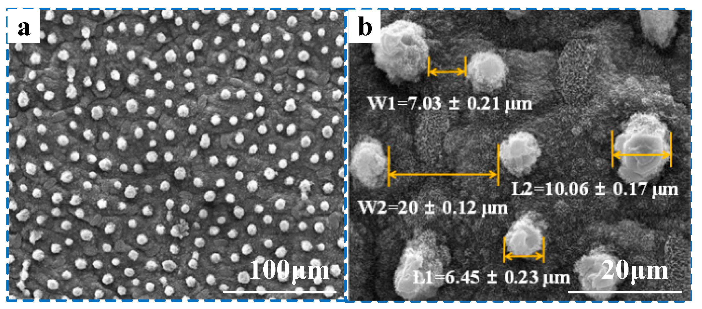
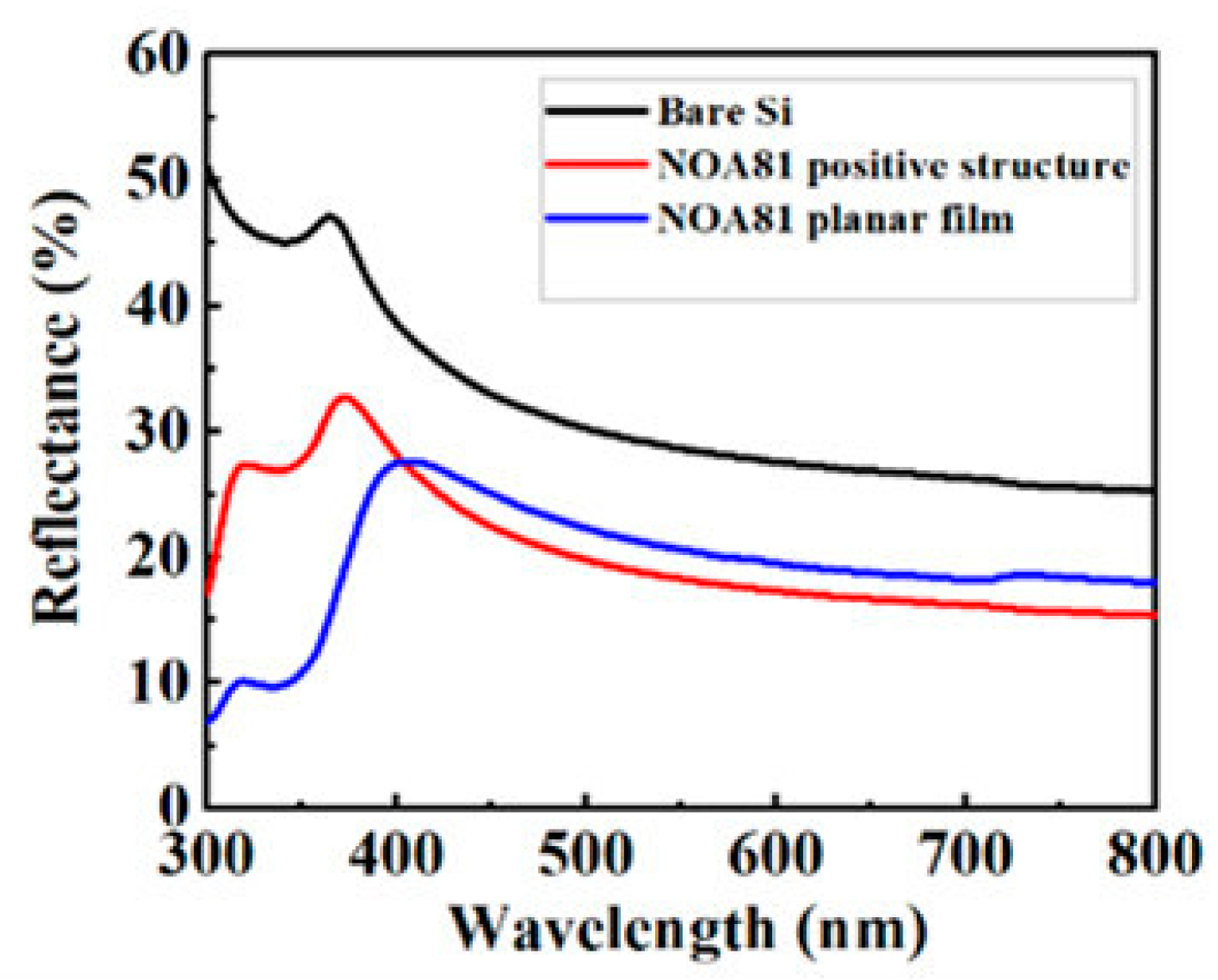
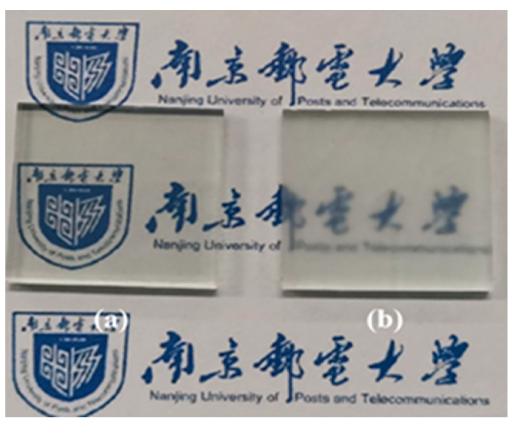
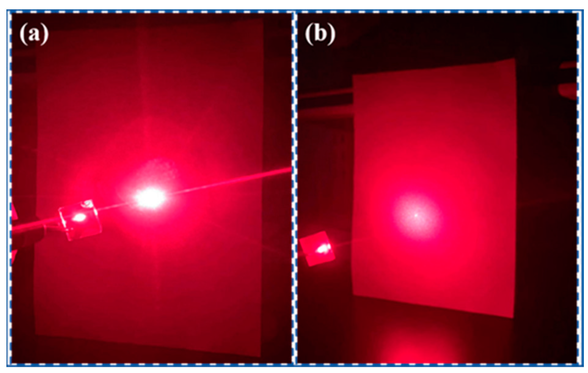
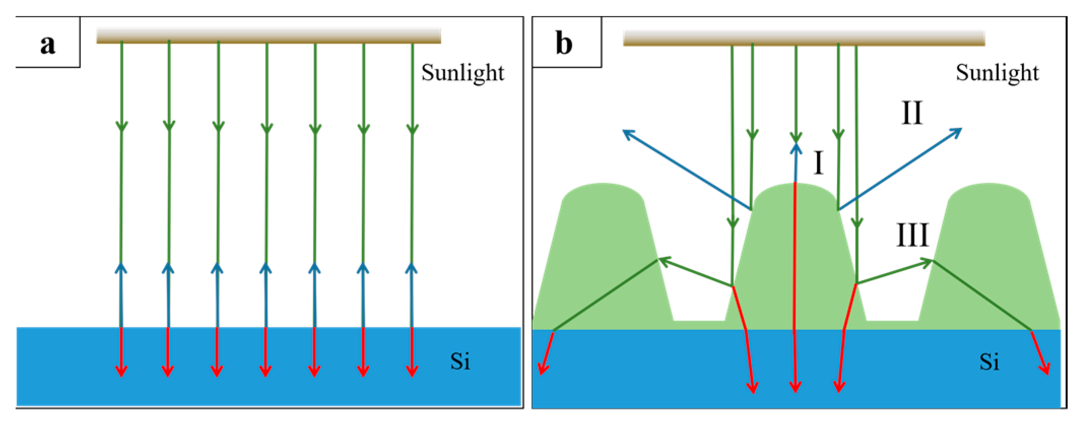
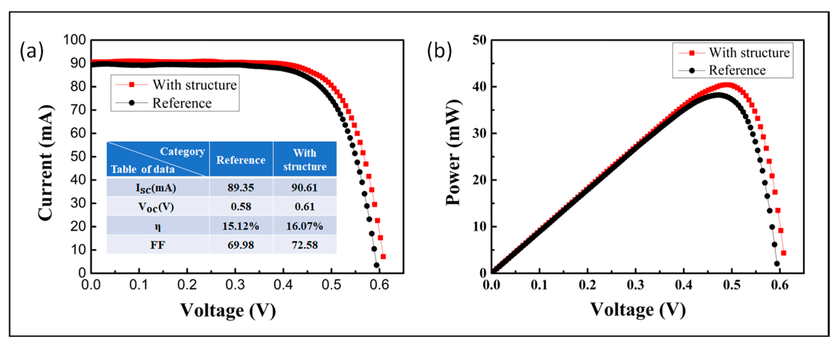
3. Results and Discussion

Figure 2 shows SEM images of the lotus leaf with (Figure 2a) small and (Figure 2b) large magnification. It can be seen from Figure 2a that there are many irregularly arranged dot-like protruding structures on the surface of lotus leaves, also called micro-papillae structures [32]. The micro-papillae vary in size, are relatively uniformly distributed, and each micro-papillae is independent of the other, which is advantageous for replicating its structure using the imprinting technique. It can be obtained from Figure 2b that the diameter ranges from L1 = 6.5 ± 0.32 μm to L2 = 8.3 ± 0.15 μm. It also can be obtained that the distance between the adjacent micro-papillae was different ranging from W1 = 7.8 ± 0.31 μm to W2 = 18 ± 0.13 μm.
Figure 3 shows SEM images of the NOA81 bionic lotus leaf structure film deposited on Si solar cells. Figure 3a–c shows the front view. Figure 3a shows the SEM image at low magnification at a scale of 50 μm. Figure 3b shows a partially enlarged image of a positively structured thin film at a scale of 20 μm. Figure 3c shows an enlarged image of a single microemulsion structure at a scale of 5 μm. The embedded image shows a magnified view from the top, with a scale of 2 μm. Figure 3 d–f shows the section view. Figure 3d shows the cross-sectional SEM image at low magnification at a scale of 50 μm. Figure 3e shows a locally enlarged image of the cross-section at a scale of 20 μm. Figure 3f shows an enlarged cross-sectional image of a single microemulsion structure at a scale of 5μm. It can be observed from Figure 3a that the film surface has a dense, irregular papillae structure, similar to that of the lotus leaf. In addition, further magnified observation of the micro-papillae are shown in Figure 3b,c, which reveal that the size of the bionic micro-papillae varies and is similar to that of the natural lotus leaves. It can be seen from Figure 3d that the bottom thickness of the NOA81 structured film was about 16.44 μm. From Figure 3e, it can be seen that the distance between the adjacent micro-papillae was different, with the spacing of W1 = 9.56 ± 2.3 μm and W2 = 17.4 ± 1.8 μm, and an average spacing of about 13.48 ± 2.1 μm. Figure 3f shows an enlarged image of the cross-section of a single micro-papillae structure. It can be seen that the bottom diameter of a single micro-papillae was about 7.46 ± 2.52 μm, and the height was about 7.12 ± 2.0 μm. It can be concluded that the size of the bionic micro-papillae is very similar to that of the natural lotus leaf, and the outline of the whole structure is a homologous vertebral parabola—a numerical simulation of homologous data [33].
Figure 4 shows the reflectance curves of the bare Si substrate, the planar NOA81 film, and the NOA81 structural film. Because the surface structure of the NOA81 structure film is a raised micro-papillae structure, we also call it NOA81 positive structure film. The curves were measured by a UV-Vis spectrophotometer with an integrating sphere in the wavelength range from 300 to 800 nm. It is clear that both NOA81 planar film and NOA81 positive structure film have lower reflectivity than bare Si, making them more conducive to improving the light absorption capacity of solar cells. In addition, in the wavelength range from 300 to 400 nm, the NOA81 positive structure film showed higher reflectivity than NOA81 planar film. We speculate that this is because NOA81 is very sensitive in the wavelength range from 320 to 380 nm, with peak sensitivity around 365 nm. In this band, the positive structural film of NOA81 improves the reflectivity of light and reduces its absorption. On the other hand, in the visible light range from 400–800 nm, the NOA81 positive structure film showed the lowest reflectance values, indicating that the bionic lotus leaf micro-papillae structure was more helpful in achieving the reflectance reduction performance.
Figure 5 shows the haze effect of the glass slides and the NOA81 structural film. It can be seen that there were test patterns of haze effect on the surface of glass slides and NOA81 structural film, respectively. By combining these results with the reflectivity curves in Figure 4, it can be found that the bionic lotus leaf micro-papillae structure increases the haze value of the film. The higher the haze value of the film, the more the observation from the film’s surface is blurred and the transparency is reduced. However, higher haze values are more conducive to reducing surface reflectivity. Therefore, we once again proved that the bionic lotus leaf micro-papillae structure was conducive to the realization of the surface anti-reflection function.
Simple light-scattering experiments were conducted on NOA81 planar films and NOA81 bionic lotus leaf positive structure films on clean glass substrate surfaces [34]. The laser diffraction imaging system was constituted of the sample to be tested, a piece of clean A4 paper, and a laser pen. The results have been shown in Figure 6. During the experiment, a clean A4 paper was used as the background plate, and a laser pen was used to illuminate the film sample about 10 cm in front. It is easy to observe that a dazzling spot appears on the background bezel of the NOA81 planar film in Figure 6a, indicating that the path of the light passing through the frictionless NOA81 planar film does not change. The light still propagates along the incident direction and finally converges on the white A4 paper, emitting a dazzling red spot. However, the diffraction rings are observed on the white baffle behind NOA81 bionic lotus leaf positive structure film in Figure 6b, indicating that the light changes directions after passing through the NOA81 bionic lotus leaf positive structure film, and a large number of light deviates from the original direction. It propagates in various directions and eventually converges on the white bezel to form some diffraction rings. The above light-scattering experiments shows that the bionic lotus leaf micro-papillae structure could change the light propagation path, which increases light scattering and reduces light reflection.
A finite-difference time-domain (FDTD) optical simulation was used to further verify the antireflection properties of the prepared NOA81 bionic lotus leaf structure, as shown in Figure 7. Figure 7a shows a model of the NOA81 bionic lotus leaf structure, with each micro-papillae having the same size. The bottom edge is 8 μm, the height is 7 μm, and the adjacent spacing is 10 μm. The base material is selected as ordinary glass with a refractive index of 1.5. Referring to the refractive index of NOA81 UV-curable adhesive, the refractive index of the micro-papillae structure is selected as 1.56. The plane wave is selected as the incident light source, and the wavelength range is from 300 to 1000 nm. Figure 7b shows the reflectivity curves of the FDTD optically simulated NOA81 bionic lotus leaf structure. It can be seen from Figure 7b that the reflectivity value of the NOA81 planar film is above 3.0%, while the reflectivity value of the NOA81 bionic lotus leaf structure is below 2.3% in the wavelength range of 300 to 1000 nm. Due to our limited experimental equipment, we could not achieve very high accuracy in the simulation experiment. During the simulation, the designed NOA81 structure film and the experimental there were some differences. Although the detailed reflectivity value had some difference with that of the experimental results in Figure 4, the results still verified that the micro-papillae structure had good anti-reflective characteristics, which also provided theoretical support for the subsequent preparation of biomimetic lotus leaf structure thin films to improve the light absorption efficiency of solar cells.
Figure 8 shows the transmission mechanism of light in silicon solar cell devices, where the green line represents light from the sun, the red line represents light absorbed by the silicon solar cell, and the blue line represents light reflected by the surface of the silicon solar cell. The surface structure of the silicon solar cell in Figure 8b is NOA81 bionic lotus leaf positive structure film. When the light is vertically incident on the bare silicon solar cell devices, it reflects back to the original path, as shown in Figure 8a. If the light hits the surface of a silicon solar cell with NOA81 bionic lotus leaf positive structure vertically, mainly three kinds of reflection paths (I, II, III) are observed, as shown in Figure 8b. Lights I and II are completely dissipated in air, and light III can be absorbed again by the silicon solar cells to improve the utilization of light energy. The local heat received by the solar cell is different due to the NOA81 bionic lotus leaf positive structure, and they can receive more heat when exposed to more sunlight.
The photovoltaic performance, including current-voltage and power, of the silicon solar cells with the NOA81 bionic lotus leaf structure has been studied with a bare silicon solar cell as the reference, and the results are shown in Figure 9. It can be seen from Figure 9a that there is no significant difference in short-circuit current (Isc) between silicon solar cells with the NOA81 bionic lotus leaf structure and the bare silicon solar cells (reference solar cell). However, the open circuit voltage (Voc) of the silicon solar cell with the biomimetic lotus leaf structure is higher than that of the reference solar cell. The increase of Fill factor (FF) further indicates that NOA81 bionic lotus leaf structure can improve the photoelectric conversion efficiency of solar cells. At the same time, the photoelectric conversion efficiency (PCE) of the silicon solar cell devices with the NOA81 bionic lotus leaf structure and the reference are 16.07% and 15.12%, respectively. with a relative improvement of about 6%. Finally, we can also find from Figure 9b that the value of the maximum power (Pmax) of the silicon solar cells with the NOA81 bionic lotus leaf structure is 41.25 mW, which was also higher than that of the reference device. It should be emphasized that the data obtained in the experiments have been rounded to two significant figures. It can be concluded that the NOA81 bionic lotus leaf structure film improves the photovoltaic efficiency of monocrystal silicon solar cells at some extent. Additionally, the structure also has the self-cleaning function as the protective film of photovoltaic devices, which would play an important role in the field of photovoltaic devices in the future.

4. Conclusions

Inspired by the surface micro-papillae structure of natural lotus leaves, we attempt to apply it to the surface of solar cells to reduce the reflectivity of the front surface. The NOA81 bionic lotus leaf structure film was successfully built on the monocrystalline silicon solar cells using the nanoimprint technique. SEM results showed that the surface structure of NOA81 thin film was almost the same as that of natural lotus leaves. The reflectivity results showed that the textured NOA81 film could effectively reduce the reflectance of the silicon wafer surface, and the FDTD simulation further verified this point. Finally, the I-V characteristics of the prepared solar cells with the textured NOA81 film were investigated, and the highest photovoltaic efficiency measured was about 16.07%. The value of the maximum power (Pmax) was 41.25 mW, effectively improving the photoelectric conversion efficiency. In the experiment, the open circuit voltage of the solar cell has been improved, but the short circuit current has not been effectively improved. For the research on short circuit current, we will continue to explore in the next experiment and finally realize the effective improvement of short circuit current. In addition, the film with the textured NOA81 can be used as a protective film for monocrystalline silicon solar cells, indicating its great application potential in the field of photovoltaic devices.

Author Contributions

Writing—review and editing, X.Z.; writing—original draft preparation, P.Z.; data curation, J.C.; project administration, W.Z. and F.H. All authors have read and agreed to the published version of the manuscript.

Funding

This work was supported by the National Natural Science Foundation of China (NSFC) (grant numbers: 61605086, 51602160, 61574080, 61274121). Natural Science Basic Research Plan in Shaanxi Province of China (Program No. 2019JM-520).

Data Availability Statement

Data underlying the results presented in this paper are not publicly available at this time but may be obtained from the authors upon reasonable request.

Conflicts of Interest

The authors declare no conflict of interest.

References

  1. Abdullah, M.F.; Alghoul, M.A.; Naser, H.; Asim, N.; Ahmadi, S.; Yatim, B.; Sopian, K. Research and development efforts on texturization to reduce the optical losses at front surface of silicon solar cell. Renew. Sust. Energ. Rev. 2016, 66, 380–398. [Google Scholar] [CrossRef]
  2. Alves, M.; Perez-Rodriguez, A.; Dale, P.J.; Dominguez, C.; Sadewasser, S. Thin-film micro-concentrator solar cells. J. Phys. Energy 2020, 2, 012001. [Google Scholar] [CrossRef]
  3. Zhang, T.; Gregoriou, V.G.; Gasparini, N.; Chochos, C.L. Porous organic polymers in solar cells. Chem. Soc. Rev. 2022, 51, 4465–4483. [Google Scholar] [CrossRef]
  4. Schygulla, P.; Heinz, F.D.; Dimroth, F.; Lackner, D. Middle Cell Development for Wafer-Bonded III-V//Si Tandem Solar Cells. IEEE J. Photovolt. 2021, 11, 1264–1270. [Google Scholar] [CrossRef]
  5. Aat, A.; Ap, B. Efficiency improvement of a silicon-based thin-film solar cell using plasmonic silver nanoparticles and an antireflective layer. Opt. Commun. 2020, 454, 124437. [Google Scholar]
  6. Yamaguchi, M.; Lee, K.-H.; Araki, K.; Kojima, N.; Ohshita, Y. Analysis for efficiency potential of crystalline Si solar cells. J. Mater. Res. 2018, 33, 2621–2626. [Google Scholar] [CrossRef]
  7. Zhao, J.; Wang, A.; Green, M.A. 24·5% Efficiency silicon PERT cells on MCZ substrates and 24·7% efficiency PERL cells on FZ substrates. Prog. Photovolt. Res. Appl. 1999, 7, 471–474. [Google Scholar] [CrossRef]
  8. Bozzola, A.; Liscidini, M.; Andreani, L.C. Broadband light trapping with disordered photonic structures in thin-film silicon solar cells. Prog. Photovolt. 2015, 22, 1237–1245. [Google Scholar] [CrossRef]
  9. Tucher, N.; Eisenlohr, J.; Gebrewold, H.; Kiefel, P.; Höhn, O.; Hauser, H.; Goldschmidt, J.C.; Bläsi, B. Optical simulation of photovoltaic modules with multiple textured interfaces using the matrix-based formalism OPTOS. Opt. Express 2016, 24, A1083–A1093. [Google Scholar] [CrossRef]
  10. Andreani, L.C.; Bozzola, A.; Kowalczewski, P.; Liscidini, M.; Redorici, L. Silicon solar cells: Toward the efficiency limits. Adv. Phys. X 2019, 4, 1548305. [Google Scholar] [CrossRef]
  11. Matsui, T.; Sai, H.; Bidiville, A.; Hsu, H.-J.; Matsubara, K. Progress and limitations of thin-film silicon solar cells. Sol. Energy 2018, 170, 486–498. [Google Scholar] [CrossRef]
  12. Suhandi, A.; Tayubi, Y.R.; Wibowo, F.C.; Arifin, P.; Supriyatman. Reducing The Light Reflected by Silicon Surface Using ZnO/TS Antireflection Coating. J. Phys. D 2017, 877, 012068. [Google Scholar] [CrossRef]
  13. Chen, L.; Wang, Y.; Qian, H.; Lu, H.; Chen, R.; Jian, Y.; Li, G.; Zhu, J.; Shi, Z.; Power, W.S. STUDY OF PERL MONOCRYSTALLINE SILICON SOLAR CELLS. Taiyangneng Xuebao/Acta Energ. Sol. Sin. 2013, 34, 2170–2174. [Google Scholar]
  14. Salman, K.A. Effect of surface texturing processes on the performance of crystalline silicon solar cell. Sol. Energy 2017, 147, 228–231. [Google Scholar] [CrossRef]
  15. Li, R.; Li, X.; Zou, T.; Fu, W.; Xing, J.; Huang, T.; Yu, Z.; Yang, J. Deep investigation of two-dimensional structure arrays formed on Si surface. Appl. Surf. Sci. 2022, 605, 154615. [Google Scholar] [CrossRef]
  16. Li, C.-H.; Zhao, J.-H.; Yu, X.-Y.; Chen, Q.-D.; Feng, J.; Sun, H.-B. Fabrication of Black Silicon With Thermostable Infrared Absorption by Femtosecond Laser. IEEE Photonics J. 2016, 8, 6805809. [Google Scholar] [CrossRef]
  17. Bian, C.; Zhang, B.; Zhang, Z.; Chen, H.; Zhang, D.; Wang, S.; Ye, J.; He, L.; Jie, J.; Zhang, X. Wafer-Scale Fabrication of Silicon Nanocones via Controlling Catalyst Evolution in All-Wet Metal-Assisted Chemical Etching. ACS Omega 2022, 7, 2234–2243. [Google Scholar] [CrossRef] [PubMed]
  18. Yamada, K.; Yamada, M.; Maki, H.; Itoh, K.M. Fabrication of arrays of tapered silicon micro-/nano-pillars by metal-assisted chemical etching and anisotropic wet etching. Nanotechnology 2018, 29, 28LT01. [Google Scholar] [CrossRef]
  19. Kumar, J.; Ingole, S. Effect of Silicon Conductivity and HF/H2O2 Ratio on Morphology of Silicon Nanostructures Obtained via Metal-Assisted Chemical Etching. J. Electron. Mater. 2017, 47, 1583–1588. [Google Scholar] [CrossRef]
  20. Zhang, B.; Jie, J.; Zhang, X.; Ou, X.; Zhang, X. Large-Scale Fabrication of Silicon Nanowires for Solar Energy Applications. ACS Appl. Mater. Interfaces 2017, 9, 34527–34543. [Google Scholar] [CrossRef]
  21. Kosloff, A.; Heifler, O.; Granot, E.; Patolsky, F. Nanodicing Single Crystalline Silicon Nanowire Arrays. Nano Lett. 2016, 16, 6960–6966. [Google Scholar] [CrossRef]
  22. Wendisch, F.J.; Rey, M.; Vogel, N.; Bourret, G.R. Large-Scale Synthesis of Highly Uniform Silicon Nanowire Arrays Using Metal-Assisted Chemical Etching. Chem. Mater. 2020, 32, 9425–9434. [Google Scholar] [CrossRef] [PubMed]
  23. Aurang, P.; Turan, R.; Unalan, H.E. Nanowire decorated, ultra-thin, single crystalline silicon for photovoltaic devices. Nanotechnology 2017, 28, 405205. [Google Scholar] [CrossRef] [PubMed]
  24. Savin, H.; Repo, P.; von Gastrow, G.; Ortega, P.; Calle, E.; Garin, M.; Alcubilla, R. Black silicon solar cells with interdigitated back-contacts achieve 22.1% efficiency. Nat. Nanotechnol. 2015, 10, 624–628. [Google Scholar] [CrossRef]
  25. Ingenito, A.; Isabella, O.; Zeman, M. Nano-cones on micro-pyramids: Modulated surface textures for maximal spectral response and high-efficiency solar cells. Prog. Photovolt. 2015, 23, 1649–1659. [Google Scholar] [CrossRef]
  26. Kanda, H.; Shibayama, N.; Uzum, A.; Umeyama, T.; Imahori, H.; Ibi, K.; Ito, S. Effect of Silicon Surface for Perovskite/Silicon Tandem Solar Cells: Flat or Textured? ACS Appl. Mater. Interfaces 2018, 10, 35016–35024. [Google Scholar] [CrossRef]
  27. Jošt, M.; Köhnen, E.; Morales-Vilches, A.B.; Lipovšek, B.; Jäger, K.; Macco, B.; Al-Ashouri, A.; Krč, J.; Korte, L.; Rech, B.; et al. Textured interfaces in monolithic perovskite/silicon tandem solar cells: Advanced light management for improved efficiency and energy yield. Energ. Environ. Sci. 2018, 11, 3511–3523. [Google Scholar] [CrossRef]
  28. Tamang, A.; Hongsingthong, A.; Jovanov, V.; Sichanugrist, P.; Khan, B.A.; Dewan, R.; Konagai, M.; Knipp, D. Enhanced photon management in silicon thin film solar cells with different front and back interface texture. Sci. Rep. 2016, 6, 29639. [Google Scholar] [CrossRef]
  29. Deng, K.; Liu, Z.; Wang, M.; Li, L. Nanoimprinted Grating-Embedded Perovskite Solar Cells with Improved Light Management. Adv. Funct. Mater. 2019, 29, 1900830. [Google Scholar] [CrossRef]
  30. Steinbach, A.M.; Kazemi, S.B.; Strehle, S. Solid-liquid-vapor etching of silicon nanostructures using hydrogen plasma. Phys. Status Solidi (A) 2016, 213, 2921–2926. [Google Scholar] [CrossRef]
  31. Manzoor, S.; Yu, Z.J.; Ali, A.; Ali, W.; Bush, K.A.; Palmstrom, A.F.; Bent, S.F.; McGehee, M.D.; Holman, Z.C. Improved light management in planar silicon and perovskite solar cells using PDMS scattering layer. Sol. Energ. Mat. Sol. C. 2017, 173, 59–65. [Google Scholar] [CrossRef]
  32. Kryuchkov, M.; Lehmann, J.; Schaab, J.; Cherepanov, V.; Blagodatski, A.; Fiebig, M.; Katanaev, V.L. Alternative moth-eye nanostructures: Antireflective properties and composition of dimpled corneal nanocoatings in silk-moth ancestors. J. Nanobiotechnol. 2017, 15, 61. [Google Scholar] [CrossRef] [PubMed]
  33. Guo, X.; Song, H.; Du, B.; Tan, S.; Liu, S. Study on Spectral Selective Manipulation Characteristics of Surface Multilevel Micro-Nano Structures by FDTD Simulation. Int. J. Mol. Sci. 2022, 23, 2774. [Google Scholar] [CrossRef] [PubMed]
  34. Zhang, X.; Bi, Y.; Liu, S.; Zhang, W.; Hu, F. Organic–Inorganic Hybrid Film MLAs Built on the Silicon Solar Cells to Improve the Photoelectric Conversion Efficiency. Coatings 2022, 12, 393. [Google Scholar] [CrossRef]
Figure 1. Preparation flow chart of NOA81 bionic lotus leaf structure film deposited on the surface of Si solar cells. (a) Lotus leaf structure; (b) Imprinting through PDMS; (c) PDMS transfer lotus leaf structure; (d) Imitation lotus leaf structure imprinted on the surface of solar cells; (e) Curing NOA81 photoresist by UV xenon lamp; (f) Remove the surface PDMS template.
Coatings 13 00867 g001
Figure 2. SEM images of the lotus leaf with (a) small and (b) large magnification.
Coatings 13 00867 g002
Figure 3. SEM images of the NOA81 bionic lotus leaf structure film deposited on Si solar cells, (ac) the front view and (df) the section view.
Coatings 13 00867 g003
Figure 4. The reflectance curves of the bare Si substrate, the planar NOA81 film, and the NOA81 structural film.
Coatings 13 00867 g004
Figure 5. The surface haze effect of (a) glass slides and (b) NOA81 bionic lotus leaf structure film.
Coatings 13 00867 g005
Figure 6. Light scattering results of (a) NOA81 planar film and (b) NOA81 bionic lotus leaf positive structure film.
Coatings 13 00867 g006
Figure 7. FDTD optical simulation of NOA81 bionic lotus leaf micro-papillae structure. (a) NOA81 bionic lotus leaf model; (b) the reflectivity curves of the simulated NOA81 bionic lotus leaf model.
Coatings 13 00867 g007
Figure 8. The transmission mechanism of light on the silicon solar cell devices. (a) a bare silicon solar cell device; (b) a silicon solar cell device with NOA81 bionic lotus leaf positive structure film.
Coatings 13 00867 g008
Figure 9. (a) I-V curves and (b) P-V curves of silicon solar cells with the NOA81 bionic lotus leaf structure compared with a bare cell.
Coatings 13 00867 g009
Disclaimer/Publisher’s Note: The statements, opinions and data contained in all publications are solely those of the individual author(s) and contributor(s) and not of MDPI and/or the editor(s). MDPI and/or the editor(s) disclaim responsibility for any injury to people or property resulting from any ideas, methods, instructions or products referred to in the content.

