Article

Microstructural and Morphological Characterization of the Cobalt-Nickel Thin Films Deposited by the Laser-Induced Thermionic Vacuum Arc Method

1
Department of Physics, Faculty of Applied Sciences and Engineering, Ovidius University of Constanta, Mamaia Av. No. 124, 900527 Constanta, Romania
2
Academy of Romanian Scientists, Ilfov No. 3, 050094 Bucharest, Romania
3
National Institute of Materials Physics, 077125 Magurele, Romania
*
Author to whom correspondence should be addressed.
Coatings 2023, 13(6), 984; https://doi.org/10.3390/coatings13060984
Submission received: 31 March 2023 / Revised: 19 May 2023 / Accepted: 19 May 2023 / Published: 25 May 2023
(This article belongs to the Special Issue Nanostructured Materials Deposition Techniques and Characterization)

Abstract

:
Laser Induced-Thermionic Vacuum Arc (LTVA) technology was used for depositing uniform intermetallic CoNi thin films of 100 nm thickness. LTVA is an original deposition method using a combination of the typical Thermionic Vacuum Arc (TVA) system and a laser beam provided by a QUANTEL Q-Smart 850 Nd:YAG compact Q-switched laser with a second harmonic module. The novelty is related to the simultaneous deposition of a bi-component metallic thin film using photonic processes of the laser over the plasma deposition, which improves the roughness but also triggers the composition of the deposited thin film. Structural analysis of the deposited thin films confirms the formation of face-centered cubic (fcc) as the main phase CoNi and hexagonal Co3Ni as the minority phase, observed mainly using high-resolution transmission electron microscopy. The magneto-optical measurements suggest an isotropic distribution of the CoNi alloy thin films for the in-plan angular rotation. From the low coercive field of Hc = 40 Oe and a saturation field at 900 Oe, the CoNi thin films obtained by LTVA are considered semi-hard magnetic materials. Magnetic force microscopy reveals spherical magnetic nanoparticles with mean size of about 40–50 nm. The resistivity was estimated at ρ = 34.16 μΩ cm, which is higher than the values for bulk Co and Ni.

1. Introduction

Cobalt-nickel alloys were recently used as a metal-organic framework (MOF) in an efficient bio-sensing platform for a series of organic building blocks for sensitive detection of miRNA, acting as metal centers or clusters [1]. Several attempts have been made using these CoNi alloys as electro-catalysts for boosting oxygen evolution; in addition, reduction reactions have been obtained due to their strong coupling properties [2]. Among the carbon nanostructures, coated ultrafine CoNi alloy nanocomposites can be used as stable trifunctional electrocatalysts for energy conversion and storage devices [3]. When CoNi alloy nanoparticles were functionalized with nitrogen-doped carbon nanostructures, the obtained nanoparticles acted as a bifunctional electrocatalyst for water splitting technologies [4].
Nevertheless, the most important application of CoNi alloys is in the field of media for magnetic or optical recording and, lately, for magnetography and MEMS applications; this is primarily due to their semi-hard magnetic properties [5]. These materials, called glass metallic or intermetallic compounds, exhibit intermediate magnetic properties between soft and hard magnets. As primarily characteristics, these alloys exhibit low coercive fields, ranging from 40 to 1000 Oe, and relatively high magnetization at saturation Ms, medium magnetization remanence Mr, and medium saturation field. These properties only require a low energy cost to magnetize different materials when compared with hard magnets, making them very useful in the magnetic recording media, but they depend on the preparation conditions, including deposition, [6] concentration [7], film thickness [8], gain size [9], and thermally annealing after deposition [10].
The coercive field is considered a nonintrinsic property, which is highly dependent on the obtained method [11,12]. More than that, the existence of two crystalline phases, the hexagonal one (P63/mmc) and the cubic one (Fm-3m), but also the interplay between the amorphous and crystalline structures, may influence the magnetic properties, including magnetization at saturation and anisotropy.
Concerning production methods, many cited studies deal with electrochemical deposition films with thicknesses varying from a few hundred nanometers up to a few microns [13,14,15]. This relatively high thickness is necessary because physical deposition techniques have largely shown poor magnetic properties for the perpendicular magnetic recording application [16,17,18].
In this context, an optimal method to obtain controlled CoNi thin films with semi-hard magnetic properties is the Laser-induced Thermionic vacuum arc (LTVA) method [19]. Using this improved technology, based on the classical Thermionic vacuum arc (TVA) method [20], the laser-induced plasma modifications provide uniform intermetallic thin films with thickness up to 100 nm with smooth surface, high purity, and tailorable surface properties.
The interplay between Thermionic vacuum arc (TVA), which produces coatings with high roughness, and the addition of the photonic processes enhances the control between the primary compounds, enabling alloys with different ratios of initial compounds to be obtained.
This paper describes a versatile method for producing CoNi thin films with semi-hard magnetic properties and controllable thickness. The interplay between hexagonal and cubic structures of Co and Ni combinations results in uniform CoNi thin films with relatively lower electrical resistivity and isotropic magnetic orientation. The deposited CoNi thin films were structurally analyzed using X-ray diffraction (XRD) and X-ray reflectometry (XRR) techniques for crystallography, thickness and density of the metallic thin films, scanning electron microscopy (SEM) and energy dispersive spectrometer (EDX) for compositional analysis, high resolution transmission electron microscope (HRTEM) for identification of crystalline phases below 5% concentration, and atomic force microscopy (AFM) and magnetic force microscopy (MFM) for the local magnetism. In addition, the magnetic and electrical properties were also investigated by the magneto-optical Kerr and four-point probe techniques.

2. Materials and Methods

2.1. The LTVA System

A schematic overview of the LTVA system is depicted in Figure 1. The LTVA configuration consists of a classical TVA device upgraded with an adjustable power laser beam. The configuration of the TVA system is presented elsewhere [21].
Briefly, TVA consists of a tungsten-heated cathode surrounded by a Wehnelt cylinder that concentrates the electron beam on the anode material. In this way, continuous evaporation of the anode material occurs and ensures the vapor density of the deposited material in the pre-breakdown state. By varying the applied high voltage between the electrodes at a certain value, bright plasma ignites. The discharge sustaining gas is simply the evaporating atoms in a vacuum. The base pressure is typically p = 4 × 10⁻⁵ Pa and the work pressure is two orders of magnitude higher throughout the deposition process. Therefore, thin film deposition occurs under high purity conditions [22]. Multicomponent thin films and single thin films were deposited using the Thermionic Vacuum Arc (TVA) method [23,24,25,26,27]. During the last decades, this technology has been successfully used for the synthesis of a large range of metals, oxides, refractory materials, and complex composites [28,29,30,31].
In the Laser-induced Thermionic Vacuum Arc–LTVA, the laser beam is provided by a QUANTEL Q-Smart 850 Nd:YAG compact Q-switched laser with a second harmonic module. The laser operates at a repetition rate of 10 Hz and the pulse-width is 5 ns for a wavelength of λ = 532 nm. The laser beam was incident on the front window of the coating chamber, exactly in the middle of the interelectrode gap. Using a pulsed laser for discrete photoexcitation of the element results in significant perturbation of the thermal energy-level distribution of those atoms.
The materials used for deposition in our experiment were Co granules (99.95%) and Ni granules (99.996%, metal basis), provided by the Alfa Aesar company, Kandel, Germany. The samples were deposited onto Si wafers (single-side silicon oxide substrates of 1 × 1 cm size). Before their introduction into the chamber, the substrates were cleaned to remove surface contamination. An ultrasonic bath with a highly effective cleaner (acetone) is the typical cleaning method. The substrate holder was grounded, and no substrate bias was applied.
The main experimental parameters are summarized in Table 1, as follows: Ua is the applied high voltage over the electrodes; Ia is the arc current, E is the energy/pulse of the laser, IL is the irradiance of the laser, If is the current of the filament heating; Ub is the breakdown voltage of the plasma; and p is the pressure inside the deposition chamber. The parameter tdep represents the deposition time and d is the thickness of the thin film measured in situ by a film thickness monitor (Cressington MTM).
To avoid other oxidative processes after deposition, the samples were allowed to cool in the deposition chamber for 24 h before any further characterization.

2.2. Analysis of the CoNi Thin Films

The diffraction patterns and thin-film reflectivity were measured using a BRUKER D8 ADVANCE type X-ray diffractometer (XRD), using CuKα1 radiation (λ = 1.54056 Å) at 40 kV and 40 mA. The analysis of the obtained patterns, such as the peak width, was performed after subtraction of Kα1 lines from the Kα1–Kα2 doublet; this was conducted with the Rachinger algorithm using the Bruker Difracplus Basic Evaluation program package [32]. The main XRD parameters were refined using Crystal Sleuth software [33] to identify the crystallographic behavior of the deposited metallic layers. The 2θ scan range was set at 30–80° with a step size of 0.05° and 0.01° resolution. Currently, Z-scan, theta rocking, and 2θ/ω steps were performed for the reflectivity of each sample.
The study of film microstructure was conducted using a Phillips CM 120 ST transmission electron microscope (TEM) equipped with HR-TEM and Selected Area Electron Diffraction (SAED) accessories. The distribution over dimensions was fitted with a log–normal function in SciDAVIS software, which gives the grain size distribution. The SAED results were used for indexing the main diffraction peaks and determining the lattice parameters. Furthermore, iTEM software (Radius 2.0 version, Emsis, Muenster, Germany) was used for imaging connected with MegaView III on the CM120ST microscope. The scratch method was used to prepare the samples for TEM analysis, and was conducted using a diamond knife and formvar-covered grids [34].
Scanning electron microscopy (SEM) and Energy-dispersive X-ray (EDX) were performed with an Evo 50 XVP with EDAX attachment (Carl Zeiss NTS) equipped with LaB6 cathode; this component works in a low vacuum mode when paired with an EDX accessory, down to 133 eV resolution.
Atomic Force Microscope (AFM) measurements were performed with an MFP-3D Stand Alone (MFP-3D-SA) microscope, enabling a scan range of XY > 90 μm and Z > 15 microns. The microscope was used in two modes: topological investigation-AFM mode and magnetic measurements-Magnetic Force Microscopy (MFM) mode. In the second mode, the phase shift Δφ of the oscillating cantilever at fixed lift height Δz was recorded. Typical dimensions of a cantilever length of 200 μm have a tip length of 4 μm, a diameter of 50 nm, and a distance of 30 nm from the surface. For MFM measurements, the cantilever tip was covered with CoCr magnetic alloy. The force on the magnetic tip is detected by measuring the displacement at the end of the cantilever, usually by optical means. An image of the magnetic stray field is obtained by slowly scanning the cantilever over the sample surface, in a raster-like fashion.
The longitudinal Magneto-Optical Kerr Effect (MOKE) was obtained using a home-made device. A beam of He-Ne laser (wavelength λ = 633 nm) through a polarizer was incident on the area around A = 3 mm2 of each magnetizing cobalt-nickel film. The reflected beam passed through the other polarizer before reaching the photodiode detector. The second polarizer, acting as an analyzer of polarization, was aligned at the angle θ with respect to the first polarizer. The variation in the reflected beam intensity (ΔIout) is directly proportional to the Kerr rotation (Δθ) and to the magnetization (M):
Δ I out = I in × sin 2 θ × Δ θ = I in × sin 2 θ × K × M
where K is a constant of experimental set-up and M is the magnetization. Typically, the MOKE curves are given as a variation of the angle between the incident and reflected light as a function of the applied magnetic field. To avoid the usage of the K constant, the hysteresis loops can be expressed in terms of magnetization normalized to the saturation magnetization (M/MS) as a function of the applied magnetic field [35].
Sheet resistances and electrical conductivities were measured using Four-Point probe equipment (Ossila) on the rectangular samples. The method is based on a current source applied on the metallic thin film between two point-like electrodes, leading to a logarithmic potential, according to the following formula:
V = I × R s 2 π × ln r
where V represents the difference in the potential between the two points situated at 1.27 mm in this study, I is the applied current, Rs is the sheet resistance, and r is the distance from the current source [36]. For a rectangular sample of 15 × 15 mm, the resistivity ρ of a thin layer material is given by:
ρ = R s × d = Δ V Δ I × π ln 2 × C × d
where d is the thickness of the thin film and C is a correction coefficient that considers the geometry of each sample [37].

3. Results

3.1. Microstructural Analysis

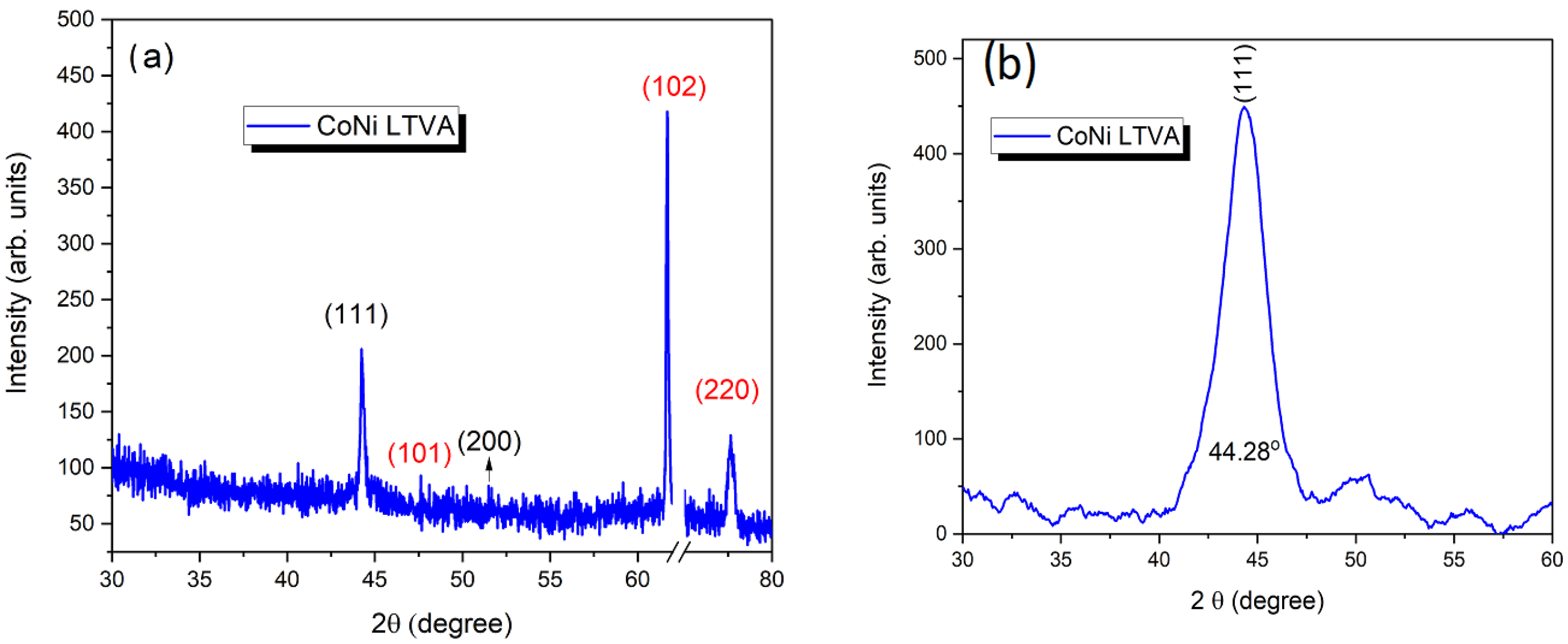
3.1.1. X-ray Diffraction

Structural analysis of the CoNi thin films obtained using LTVA method was characterized using X-ray diffraction methods. Two peaks are observed in 2 θ scanning at 44.28°, which can be indexed as (111) plane of face-centered cubic (fcc) phase CoNi (JCPDS no. 15–0806 for fcc Co, JCPDS no. 04–0850 for fcc Ni, respectively) [38]. As shown in Figure 2, another small peak can be revealed at 51.58°, indexed as (200).
The zone between 65° and 75° degrees was arbitrarily removed to hide the XRD peaks of the Si substrate, centered at 69°. The peak from 44.28° can vary between 44.2° for a pure fcc Co structure to 44.28° in the case of Co3Ni and at 44.4° for CoNi3 [39,40].
Interestingly, the second phase, marked by diffraction on the (102) plane, was observed at 62.55° as well as a possible one at 47.66°, indexed as (101). All peaks are indexed in Table 2.

3.1.2. HRTEM and SAED Measurements

The XRD results were verified using High-Resolution Transmission Electron Microscopy (HRTEM) with the aid of Selected Area Electron Diffraction (SAED), a more sensitive method that allows a better estimation of the crystallite dimensions.
The HRTEM image shows a uniform thin film (Figure 3) with a crystallite dimension of about Lc = 5 nm, estimated using a lognormal distribution of Feret’s diameter, the algorithm implemented in the iTEM platform (right inset Figure 3). The left inset shows the electron diffraction and Miller indices for Ni or Co cubic system [41].
The profile extracted from electron diffraction pattern was used to evaluate the lattice parameters of cubic Ni, Co, and hexagonal Co3Ni. Table 3 shows the peaks identified from the profile and Scherrer analysis of the crystalline size [42,43].
The values of crystalline sizes reported from XRD analysis are very well correlated with crystallite sizes estimated from TEM images.
The ratio of lattice parameters a/c is revealed in Table 4, according to the cubic structure of Ni and Co. Additionally, the lattice parameter was refined using a modified Cohen method with a Nelson–Riley function applied to the electron diffraction (cosθ ≈ 1 and sinθ ≈ θ) [44]. This ratio, estimated from the Cohen method, agrees well with the measured value a/c = 3.4951 Å, with a 1.31% error for Ni and a 2.19% error for Co.

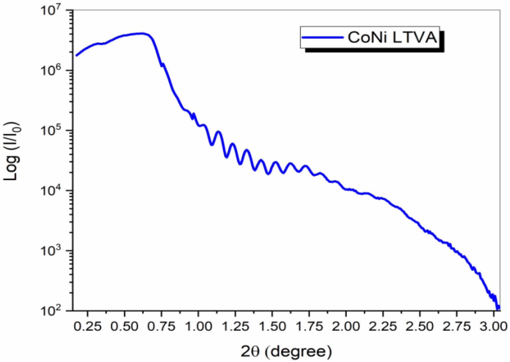
3.2. X-ray Reflectometry

The thickness and roughness of the CoNi thin films were obtained by X-ray reflectometry (XRR) with good resolution, using 0.2 mm slits for both X-ray tube and detector. The 2 θ/omega patterns can be seen in Figure 4.
The XRR patterns were analyzed with REFLEX software, considering a multilayer structure formed from silicon/SiO2/Co-Ni/Co-Ni oxide [45]. The curve exhibits two main critical angles at 0.32° and 0.67°. The most important one (0.67°) is associated with the density of Co-Ni thin film. This critical angle is the same for both metals (Co and Ni) because they have similar densities (Co: density = 8.9 g cm−3; Ni: density = 8.908 g cm−3) [46]. The critical angle from 0.32° was assigned to cobalt-nickel oxide layer with a mean density of 6.44 g cm−3. A thin oxide layer gives a broad peak between 1.5° and 3° with a thickness of 7 nm; this was obtained from the fitting procedure.
The maxima/minima between 1° to 1.75° are assigned to the CoNi thin film; based on the Bragg formula, the distances between two maxima/minima give the thickness of the layer, estimated at 95 ± 5 nm. The roughness of the CoNi thin film is around R = 1.8–2 nm; this was confirmed by the AFM measurements.

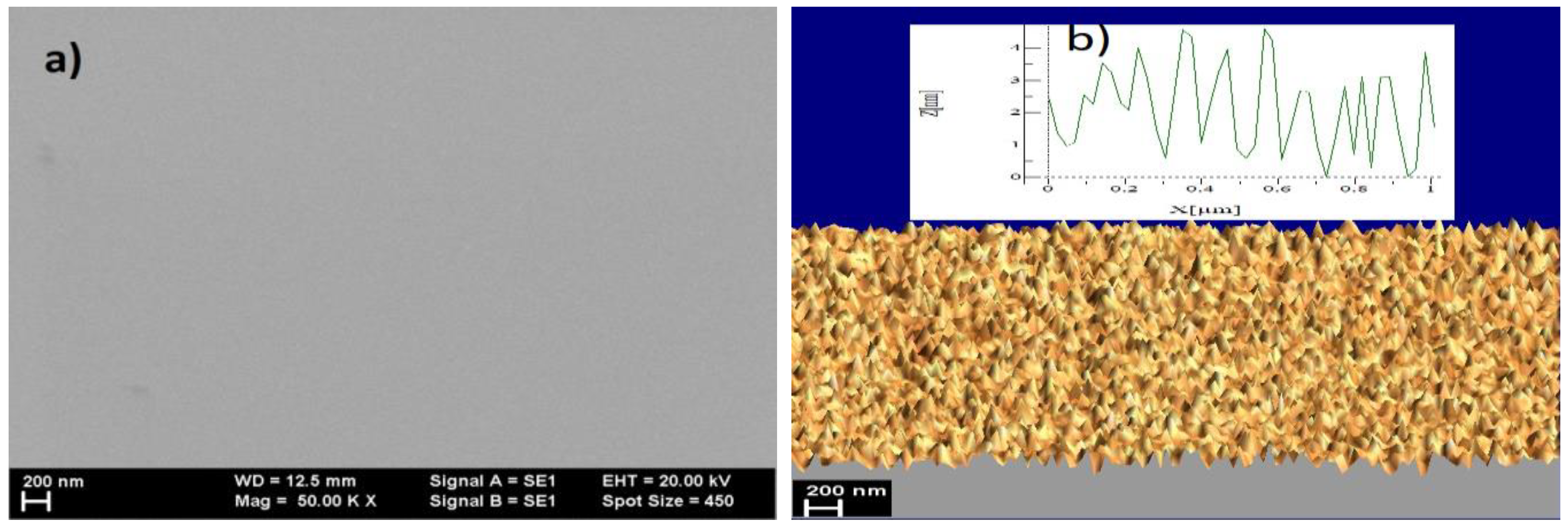
3.3. SEM and EDX Analysis

The SEM image of the surface morphology of CoNi thin films grown on silicon substrate is shown in Figure 4. The surface of the CoNi thin films on an area of about 3 × 3 μm looks smooth, proving the superior characteristics of deposition by the LTVA method (Figure 5a).
In the 3D image with a length of 1 µm, the CoNi surface has an average roughness of about Ra = 4 nm, resulting in a good agreement with the fitting procedure of XRR patterns (Figure 5b).
More interesting is the EDX analysis, which gives information about the composition of the deposited thin films. It also shows where the main peaks are assigned to Co, Ni, and larger Si substrate, and shows that they are accompanied by traces of oxygen and carbon K-lines (Figure 6).
If the line 0.776 keV of Co is superimposed on 0.851 keV line of Ni, the line 6.929 keV of Co is well separated by one at 7.477 keV of Ni on the wide spectrum. The traces of carbon are due to the carbon crucible used during LTVA deposition. The concentrations measured at three points of the CoNi thin film are given in Table 5.
As can be seen, the Ni/Co concentrations in all three points have a mean value of 2.3–2.5; this ratio that suggests an amorphous Co/Ni, but with partial crystalline structures, as can be seen in XRD and TEM.

3.4. Surface and Magnetic Properties

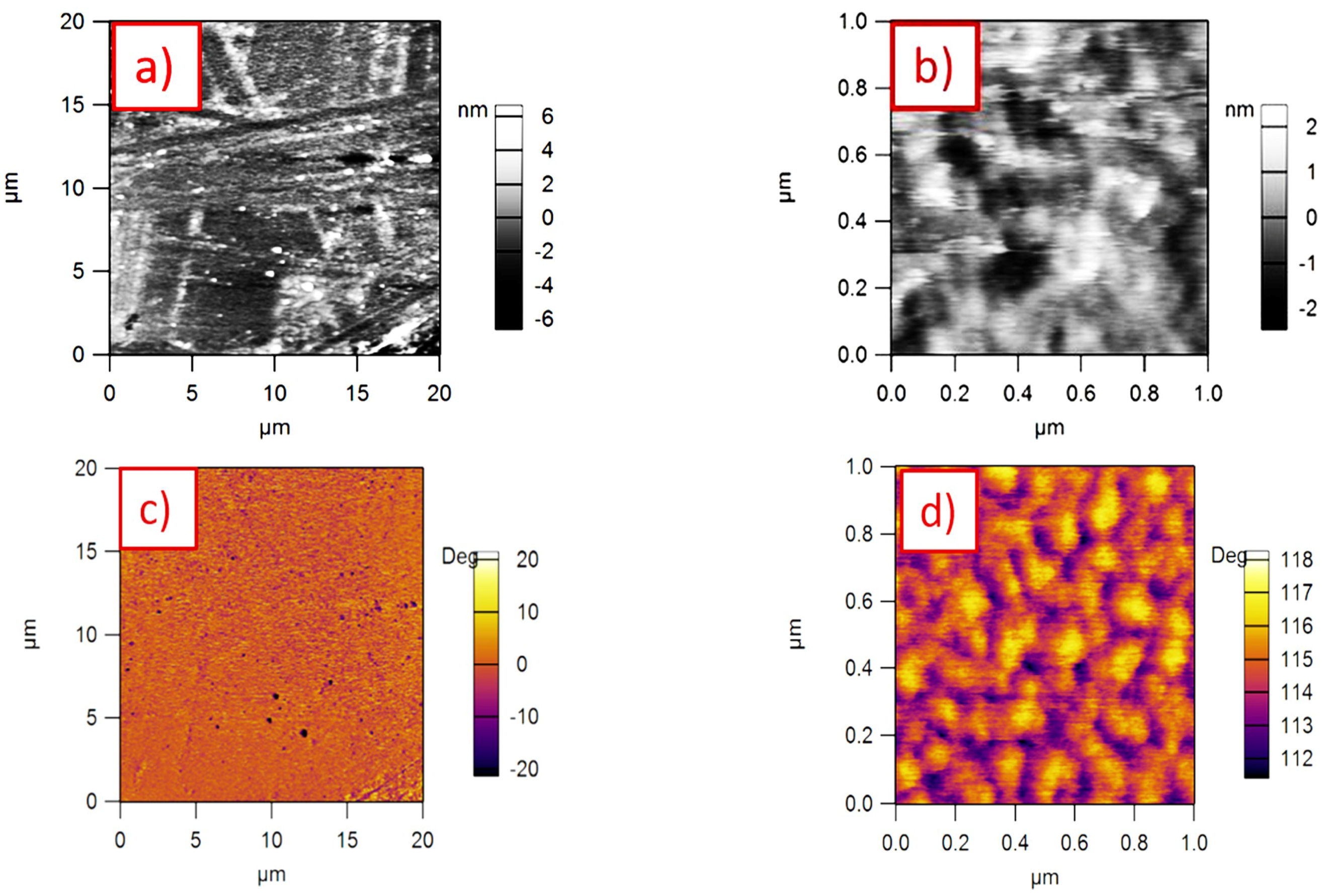
3.4.1. Atomic and Magnetic Force Microscopy

Atomic force microscopy (AFM) and magnetic force microscopy (MFM) were investigated at different scaling square zones: 20 × 20 μm (a, c) and 1 × 1 μm (b, d) (Figure 7).
At a large scale, the roughness was confirmed to be Ra = 6.68 nm (Figure 7a); at a small scale, the roughness is reduced to 4.5 nm (Figure 7b). This is the most interesting image because it shows some spherical particles with a mean size of about 40–50 nm.
The morphology and the shape of these particles were confirmed by magnetic force microscopy (MFM) measurements. In magnetic force microscopy (MFM), the magnetic field is detected by placing a small magnetic tip, usually covered with CoCr alloys, on a cantilever spring, close to the surface of the thin film. The scan areas follow AFM images from 20 × 20 μm to 1 × 1 μm, with a recording time between 5 and 30 min (Figure 7c,d).
In this study, we used CoCr cantilevers with a radius of less than 40 nm and a scan rate of 1 Hz. In standard Magnetic Force Microscopy measurements, the phase shift Δφ of the oscillating cantilever is recorded at a fixed lift height Δz [47].
The phase shift Δφ marks the magnetic interaction between the tip and the CoNi thin film, where this magnetic interaction is related to the gradient ∂F/∂z along the z-direction perpendicular to the surface plane of the component along z of the long-range interaction force Fz through the relation:
Δ φ = Q c k c × F z z
where Qc and kc are the quality factors of the cantilever first resonance in air and the cantilever spring constant, respectively [48].
In Figure 7d, the same 40–50 nm magnetic particles can be easily identified; this confirms the magnetic characteristics of CoNi thin films. These behaviors have been further studied using the longitudinal magneto-optical Kerr effect, as shown in the next section.

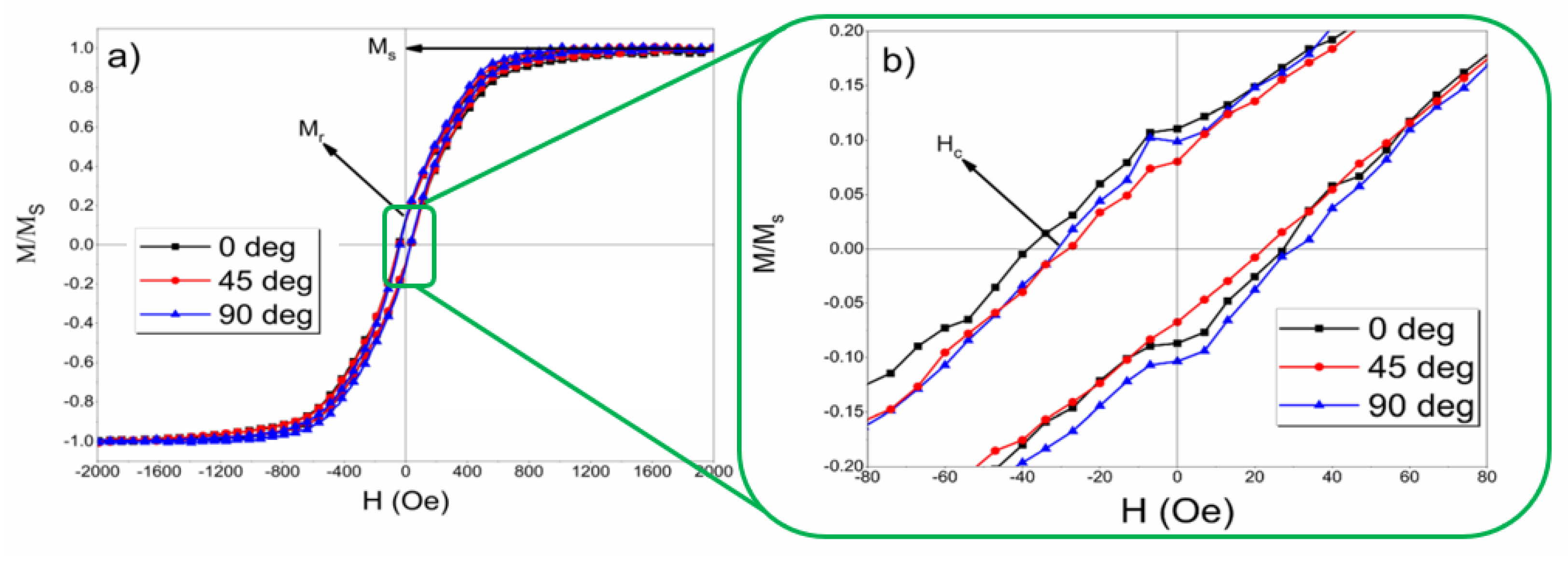
3.4.2. Longitudinal MOKE Method

The hysteresis loops from the longitudinal magneto-optic Kerr effect (MOKE) magnetometry were recorded with the magnetic field oriented parallel with the CoNi surface of the sample (in-plane analysis). Even if the hysteresis loops differ from the typical characteristics of classical magnetic measurements, this effect can be used to study the local magnetism of magnetic thin films. Here, a hysteresis loop is a plot of the magnetization as a function of the applied magnetic field on the CoNi thin film. The magnetic field was established between H = −2000 Oe and H = 2000 Oe in order to determine the saturation of the magnetization effect.
The magnetic behavior observed in the magnetic force microscopy was confirmed in the MOKE measurements presented in Figure 8a,b.

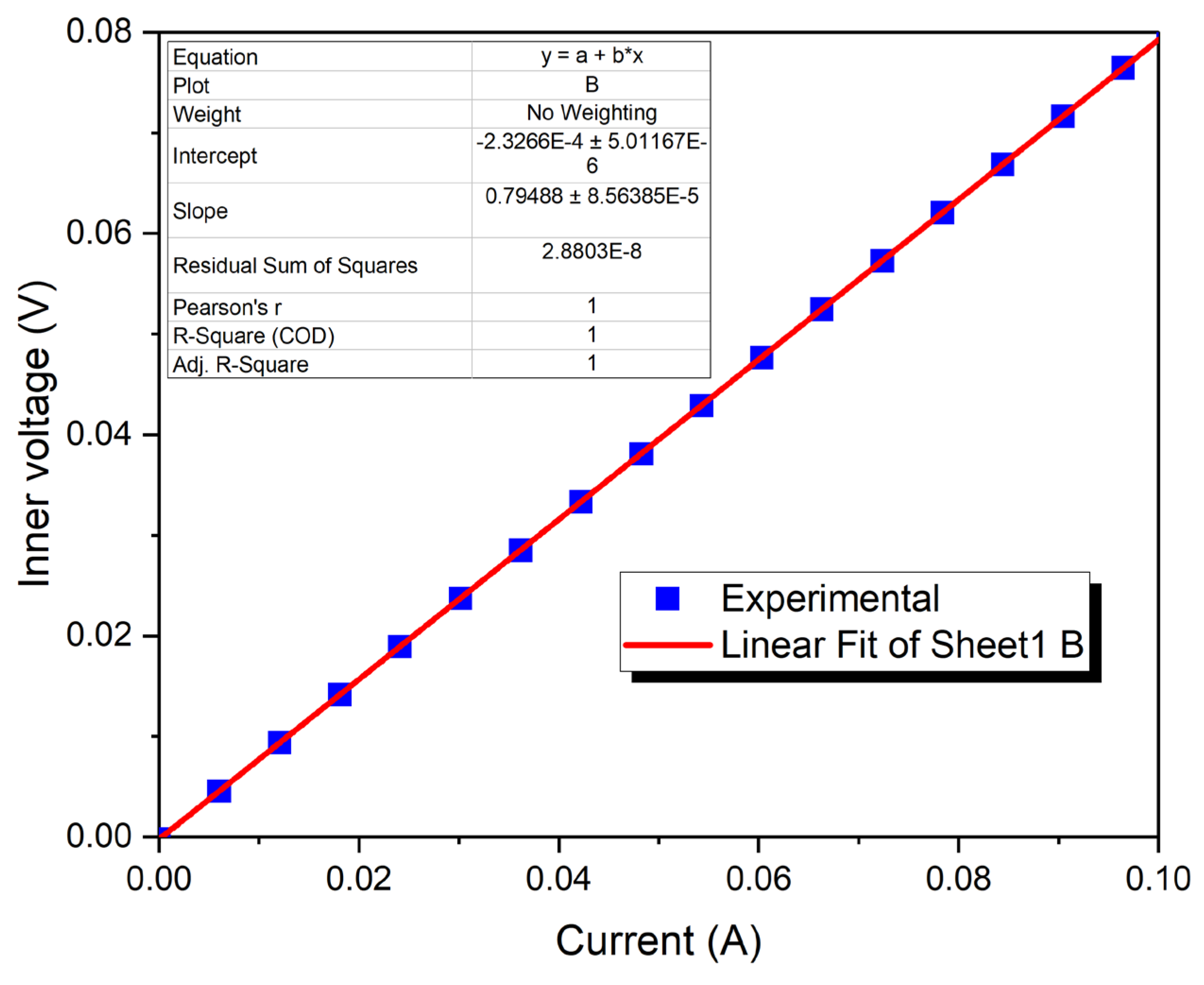
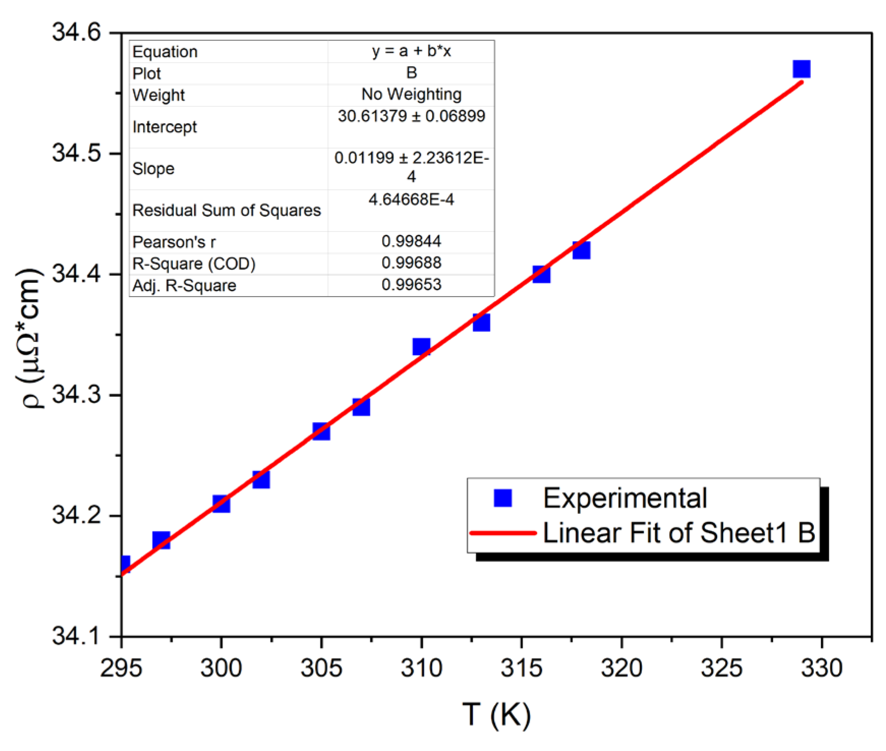
3.5. Electrical Measurements

Electrical measurements follow two aspects: (a) measurements of the sheet resistance and, based on the estimated thickness and geometry of the sample, determination of the resistivity for the CoNi thin layer, and (b) dependence of the resistivity with heating of samples in the range T = 295−329 K.
The sheet resistance was measured between the applied current and the inner voltage of the four-point probe equipment (Figure 9).
Using the four-point probe technique, the applied voltage on the outer electrodes combined with the high internal resistance of the equipment allows only the current injection in the metallic thin films, while the measured voltage on the inner electrodes avoids the contact resistance between the electrodes and the metallic thin film. In this way, an accurate measurement of the sheet resistance can be controlled in thin films with thicknesses up to 1 mm.
The slope of the linear dependence between the inner voltage and applied current gives the sheet resistance and, by applying Formula (3), the resistivity was estimated at ρ = 34.16 μΩ cm.
When the sample is heated, the resistivity varies linearly with temperature between T = 295 K and T = 329 K (Figure 10).
The resistivity versus applied temperature follows a linear dependence just over room temperature, given by:
ρ = ρ 0 1 + α × Δ T
where α is the temperature coefficient expressed as 1/°C and ρ o is the resistivity at room temperature. From the linear slope, the temperature coefficient is α = 11.99 × 10⁻³ C−1.

4. Discussions

For Co-Ni alloys, it is important to discuss their phase diagram because solidification occurs in a temperature interval of only a few degrees [49]. In this context, the solid equilibrium between Co and Ni exhibits a complete solid solution in the α (Fm-3m) phase at temperatures between the solidus and the allotropic transformation temperature of the α to ε (P63/mmc) phase. The phase appears in the whole range of Ni dissolution in Co from 0 to 100 at.% Ni, but the ε (P63/mmc) appears between 0 and 35 at.% of Ni.
Several papers describe the Co-Ni alloys as a combination of cubic Ni (Fm-3m) and cubic Co (Fm-3m), proving the presence of Ni atoms by the shift of the (111) peak position of Co from 44.201° in pure Co nanoparticles [50,51] to 44.469° in the case of pure Ni nanoparticles [38]. For the Co:Ni (3:1) composition, the peak shift is up to 44.280°. However, the intensities of (111) for the cubic structure and (102) for the hexagonal one, together with the lower intensities for the (101) and (200), confirm a preferential orientation of crystallites in the amorphous matrix.
The hexagonal structure of the Co3Ni system (Co0.75Ni0.25) has bigger errors, so the probability of finding such a system in the sample is low. However, the intensity of the (102) peak reflection justified the presence of the oriented hexagonal structure.
The grain size of the crystalline structure for the Co or Ni metals can be evaluated using the Debye–Scherrer formula, accounting for the broadening of the equipment based on the Si (100) from 69.3°. The mean value of crystallites is around 3–4 nm.
From the XRR, the thickness and density of metallic thin films can be estimated. The film thickness, around 95 nm, is in good agreement with the measured one with the quartz balance during thin film processing. The film density was estimated to 6.44 g cm−3, compared with 8.9 g cm−3 for Co and 8.91 g cm−3 for Ni. The estimation of the relative porosity is the ratio (dmetal − dfilm)/dmetal, where dmetal is the density of the pure Co or Ni crystalline film and dfilm is the density of the Co3Ni film [52]. This fact leads to a relative porosity of 27.5%.
The cell parameter, determined from the X-ray diffraction patterns for the CoNi composition of about 3.4084 nm, was confirmed by the HRTEM and SAED images, where the profile extracted from the electron diffraction pattern was used to evaluate the lattice parameters of cubic Ni, with Co giving a closed value of about 3.38 nm. However, the HRTEM images confirm the presence of hexagonal Co3Ni with a more accurate precision when compared with the XRD measurements.
The surface images obtained using the SEM technique reveal a smooth surface in the 2D dimension, while the roughness from 3D images varies between 2 and 4 nm. This fact explains the advantages of the LTVA technique over the classical TVA method, where the roughness covers tens of nanometers.
EDX analysis at three points of the CoNi film confirms the ratio of Co:Ni around 3:1 and justified the presence of Co3Ni hexagonal structure observed in SAED and XRD measurements.
The AFM measurements confirm the low roughness of the CoNi thin films on the extended area of about 20 × 20 µm (around 7 nm); in the small area of 1 × 1 µm, the roughness is 4.5 nm in a good agreement with the X-ray reflectivity measurements.
Magnetic force microscopy (MFM) reveals large domains of magnetization of about 40–50 nm; these are probably a mix between the crystalline structures with the amorphous Co and Ni.
The measurement of magnetization (M) is connected with the rotation of the polarization plane of light as it is reflected at the sample surface. This can be phenomenologically described by:
D = ϵ × E + i × Q × M × E
where D is the induced displacement vector, ε is the dielectric constant, E is the electrical vector of the incoming plane light wave, i is the imaginary part, and Q is a material parameter. The cross-product M × E links the magnetization with the change in the displacement vector and thus the electrical vector of the reflected light wave [53]. Commonly, the magnetic signal is measured as a variation of the angle between the incident and reflected light as a function of the applied magnetic field, θ = f(M(H)).
From the longitudinal MOKE measurements, the CoNi thin films with a mean thickness of about 100 nm have a coercive field of about Hc = 38–42 Oe, depending on the orientation in-plane of the sample (Figure 8b) and a saturation field of around Ms = 900 Oe. The angular dependence of the magnetization with the rotational angle indicates an isotropic magnetic thin film without specific magnetization domains, supported by the amorphous structure of the CoNi thin films.
Considering only the coercive field, the obtained CoNi thin films should be seen as soft materials, but the saturation field is higher than similar cobalt thin films obtained by thermal evaporation, which has a saturation field of around Ms = 130–150 Oe [36].
If we consider the squareness of the in-plane field hysteresis loop defined as the ratio between the remanent magnetization and saturation (Mr/Ms), the obtained value is around 0.15. This value is smaller than the 0.4 obtained in the Co1−xNix with x = 25%, 1 μm-thick film of CoNi alloys deposited using the sputtering technique [54]. The coercive field is slightly lower than that in the case of Co1−xNix for all Ni at.% concentrations for which the coercive field is over Hc = 100 Oe. In this context, our CoNi thin films can be seen as semi-hard magnetic materials with a coercive field ranging from 50 to 1000 Oe [5].
In most cases, the thin film resistivity ( ρ f) is highly dependent on the film thickness. The increase in resistivity, defined as Δ =   ρ f- ρ bulk, is proportional to 1/d, where ρ bulk is the bulk resistivity and d is the film thickness [55]. Many theories have been proposed to analyze experimental thin-film resistivity as a function of the thickness, but the most common is the one based on the grain boundary scattering model, developed by Mayadas et al. [56], which was successfully applied to cobalt and nickel thin films. This model can be applied considering thin polycrystalline layers; the amount of surface scattering is relatively small. In this context, thin-film resistivity depends on the bulk resistivity and a constant γ, which considers the size effects:
ρ film = 1 d ρ bulk × d + γ
where γ depends on the ratio between the grain size diameter D and film thickness d.
The value of resistivity ( ρ = 34.16 μΩ cm for the CoNi thin films obtained by the LTVA method) agrees well with similar cobalt thin films thermally evaporated on the silicon substrate. For these films, the resistivity varies from ρ = 98 μΩ cm (thickness d = 10 nm) up to ρ = 43.14 μΩ cm for d = 100 nm thin film, having 1/d dependence [57]. These values are higher than the bulk resistivity for bulk Co ( ρ = 5.88 μΩ cm) or Ni ( ρ = 7.14 μΩ cm) [47].
The effective resistivity of a metal follows Matthiessen’s rule and the change in the resistivity, due to a small increase in ΔT, is temperature independent, enabling the linear approximation [58]. For the range above 100 K up to 1000 K, all metals exhibit linear resistivity versus temperature [59]. The temperature coefficient is larger when compared with the individual bulk metals, which are α = 6.6 × 10⁻³ (K−1) for Co and α = 6.5 × 10⁻³(K−1) for Ni. This fact can be explained by the same dependence of resistivity versus film thickness for metallic thin films.

5. Conclusions

The LTVA method is a new and reliable method for production of thin films with tailorable properties, in this case, intermetallic Co-Ni compound with a crystalline structure, due to the enhanced rate of collisional ionization of the resulting excited state atoms relative to the ground state. The obtained films have semi hard magnetic structures with low coercive field and medium magnetization characteristics.
This novel method allows simultaneous deposition of a bi-component metallic thin film using photonic processes of the laser over the plasma deposition, which improves the roughness but also the composition of the deposited thin film. The resulting CoNi thin films exhibit a mixture of crystalline phases with a large amorphous compound that influences the electrical and magnetic properties of these films. The roughness of these films is lower than those deposited with the TVA method or other thermal evaporation methods.
The electrical resistivity is higher than the bulk CoNi alloys, justified by the grain boundary scattering model with fcc cubic structures for pure Co and Ni nanocrystals with a small amount of hexagonal Co3Ni nanocrystals. Just above room temperature, the electrical resistivity shows a higher thermal coefficient influenced by the relatively small thin film thickness.
The magnetic images based on the phase shift Δφ from the MFM measurements showed spherical magnetic particles with a mean size of about 40–50 nm. The Moke measurements suggest an isotropic distribution of the magnetic nanoparticles for the in-plan angular rotation.

Author Contributions

Conceptualization, R.V. and S.P.; methodology, S.P.; investigation, V.C., A.M., G.P. and V.D.; writing—original draft preparation, S.P.; writing—review and editing, R.V. All authors have read and agreed to the published version of the manuscript.

Funding

This research was funded by Intermediary Body-Romanian Ministry of Research and Innovation, grant number 54/2016, SMIS code 105726, POC-G project MAT2IT.

Institutional Review Board Statement

Not applicable.

Informed Consent Statement

Not applicable.

Data Availability Statement

Not applicable.

Conflicts of Interest

The authors declare no conflict of interest.

References

  1. Hu, M.; Zhu, L.; Li, Z.; Guo, C.; Wang, M.; Wang, C.; Du, M. CoNi bimetallic metal–organic framework as an efficient biosensing platform for miRNA 126 detection. Appl. Surf. Sci. 2021, 542, 148586. [Google Scholar] [CrossRef]
  2. Gui, L.; Pan, G.; Ma, X.; You, M.; He, B.; Yang, Z.; Sun, J.; Zhou, W.; Xu, J.; Zhao, L. In-situ exsolution of CoNi alloy nanoparticles on LiFe0.8Co0.1Ni0.1O2 parent: New opportunity for boosting oxygen evolution and reduction reaction. Appl. Surf. Sci. 2021, 543, 148817. [Google Scholar] [CrossRef]
  3. Xie, Y.; Feng, C.; Guo, Y.; Li, S.; Guo, C.; Zhang, Y.; Wang, J. MOFs derived carbon nanotubes coated CoNi alloy nanocomposites with N-doped rich-defect and abundant cavity structure as efficient trifunctional electrocatalyst. Appl. Surf. Sci. 2021, 536, 147786. [Google Scholar] [CrossRef]
  4. Li, R.; Li, X.; Liu, C.; Ye, M.; Yang, Q.; Liu, Z.; Xie, L.; Yang, G. Enhanced electron transport through a nanoforest-like structure of CoNi nanoalloy@nitrogen-doped carbon nanotubes for highly efficient catalysis of overall water splitting. Appl. Surf. Sci. 2020, 517, 145841. [Google Scholar] [CrossRef]
  5. Cullity, B.D.; Graham, C.D. Introduction to Magnetic Materials, 2nd ed.; Wiley Hoboken: New Jersey, NJ, USA, 2009; pp. 154–196. [Google Scholar]
  6. Kefalas, J.H. Effect of electroplating parameters on magnetic properties of Ni-Co alloys. J. Appl. Phys. 1966, 37, 1160. [Google Scholar] [CrossRef]
  7. Tutovan, V.; Velican, N. Magnetic properties of electrodeposited Ni-Co thin films. Thin Solid. Film. 1971, 7, 219–227. [Google Scholar] [CrossRef]
  8. Tutovan, V.; Velican, N. Stripe domains in electrodeposited NiCo thin films. Thin Solid. Film. 1973, 15, 31–37. [Google Scholar] [CrossRef]
  9. Rhen, F.M.F.; Roy, S. Dependence of magnetic properties on micro- to nanostructure of CoNiFe films. J. Appl. Phys. 2008, 103, 103901. [Google Scholar] [CrossRef]
  10. Wu, C.; Wang, K.; Li, D.; Lou, C.; Zhao, Y.; Gao, Y.; Wang, Q. Tuning microstructure and magnetic properties of electrodeposited CoNiP films by high magnetic field annealing. J. Magn. Magn. Mater. 2016, 416, 61–65. [Google Scholar] [CrossRef]
  11. Ducharme, S.; Fridkin, V.M.; Bune, A.V.; Palto, S.P.; Blinov, L.M.; Petukhova, N.N.; Yudin, S.G. Intrinsic Ferroelectric Coercive Field. Phys. Rev. Lett. 2000, 84, 175–178. [Google Scholar] [CrossRef]
  12. Jo, J.Y.; Kim, Y.S.; Noh, T.W.; Yoon, J.G.; Song, T.K. Coercive fields in ultrathin BaTiO3 capacitors. Appl. Phys. Lett. 2006, 89, 232909. [Google Scholar] [CrossRef]
  13. Thanikaikarasan, S.; Mahalingam, T.; Ahamad, T.; Alshehri, S.M. Role of substrate on film thickness, structural, compositional and magnetic properties of CoNi alloy thin films by low temperature electrodeposition technique. J. Saudi Chem. Soc. 2020, 24, 955–962. [Google Scholar] [CrossRef]
  14. Chena, Q.S.; Zhou, Z.Y.; Guo, G.C.; Sun, S.G. Electrodeposition of nanostructured CoNi thin films and their anomalous infrared properties. Electrochim. Acta 2013, 113, 694–705. [Google Scholar] [CrossRef]
  15. Park, D.Y.; Song, R.Y.; Ko, J.M.; Yoo, B.Y.; Myung, N.V. Stress Changes of Nanocrystalline CoNi Thin Films Electrodeposited from Chloride Baths. Electrochem. Sol. State. Lett. 2005, 8, C23–C25. [Google Scholar] [CrossRef]
  16. Yamaguchi, H.; Yanagisawa, M. Magnetic properties and structures of sputtered CoNi/Cr films. IEEE Trans. Magn. 1986, 22, 576–578. [Google Scholar] [CrossRef]
  17. Lee, H.J. The crystal growth and magnetic properties of sputtered CoNi films on bcc polycrystalline underlayers. J. Appl. Phys. 1988, 63, 3269. [Google Scholar] [CrossRef]
  18. Spencer, A.G.; Howson, R.P. The properties of magnetron sputtered CoNi thin films. Vacuum 1986, 36, 103–105. [Google Scholar] [CrossRef]
  19. Vladoiu, R.; Mandes, A.; Dinca, V.; Kudrna, P.; Tichý, M.; Polosan, S. Magnesium-silver cathodes for efficient charge-injection into Organic Light Emitting Diodes deposited by LTVA method. J. Alloy. Comp. 2021, 869, 159364. [Google Scholar] [CrossRef]
  20. Vladoiu, R.; Tichý, M.; Mandes, A.; Dinca-Balan, V.; Kudrna, P. Thermionic Vacuum Arc—A versatile technology for thin film deposition and its applications. Coatings 2020, 10, 211. [Google Scholar] [CrossRef]
  21. Ekem, N.; Musa, G.; Pat, S.; Balbag, Z.; Cenik, I.; Vladoiu, R. Carbon thin film deposition by Thermionic Vacuum Arc (TVA). J. Opt. Adv. Mater. 2008, 10, 672–674. [Google Scholar]
  22. Staicu, C.; Locovei, C.; Dinu, A.A.; Burducea, I.; Butoi, B.; Pompilian, O.G.; Porosnicu, C.; Lungu, C.P.; Kuncser, V. Structural and Magnetic Specificities of Fe-B Thin Films Obtained by Thermionic Vacuum Arc and Magnetron Sputtering. Coatings 2022, 10, 1592. [Google Scholar] [CrossRef]
  23. Durmus, C.; Akan, T. Vanadium pentoxide thin films deposited by the thermionic vacuum arc plasma. Thin Solid. Film. 2023, 770, 139764. [Google Scholar] [CrossRef]
  24. Lungu, C.P.; Mustata, I.; Musa, G.; Lungu, A.M.; Brinza, O.; Moldovan, C.; Rotaru, C.; Iosub, R.; Sava, F.; Popescu, M. Unstressed carbon-metal films deposited by thermionic vacuum arc method. J. Opt. Adv. Mater. 2006, 8, 74–77. [Google Scholar]
  25. Kuncser, V.; Valeanu, M.; Scanteie, G.; Filoti, G.; Mustata, I.; Lungu, C.P.; Anghel, A.; Chiriac, H.; Vladoiu, R.; Bartolomeu, J. Exchange Bias and spin valve systems with Fe-Mn antiferromagnetic prinning layers, obtained by TVA method. J. Magn. Magn. Mater. 2008, 320, e226–e230. [Google Scholar] [CrossRef]
  26. Pat, S.; Celik, O.; Odabas, A.; Korkmaz, S. Optical properties of Nb2O5 doped ZnO nanocomposite thin film deposited by thermionic vacuum arc. Optik 2022, 258, 168928. [Google Scholar] [CrossRef]
  27. Vladoiu, R.; Mandes, A.; Dinca-Balan, V.; Prodan, G.; Kudrna, P.; Tichý, M. Magnesium plasma diagnostics by heated probe and characterization of the Mg thin films deposited by thermionic vacuum arc technology. Plasma Sources Sci. Technol. 2015, 24, 035008. [Google Scholar] [CrossRef]
  28. Mandes, A.; Vladoiu, R.; Dinca, V.; Prodan, G. Binary C-Ag Plasma Breakdown and Structural Characterization of the Deposited Thin Films by Thermionic Vacuum Arc Method. IEEE Trans. Plasma Sci. 2014, 42, 2806–2807. [Google Scholar] [CrossRef]
  29. Vladoiu, R.; Ciupina, V.; Contulov, M.; Mandes, A.; Dinca, V.; Prodan, G.; Lungu, C.P. Structure and tribological properties of carbon-based nanocomposites grown by TVA method. J. Opt. Adv. Mater. 2010, 12, 553–556. [Google Scholar]
  30. Ozkan, M.; Erdem, S.S.; Mohammadigharehbagh, R.; Kurtaran, S.; Pat, S. Investigation of substrate effect on Co-doped ZnO thin films prepared by thermionic vacuum arc technique. Inorg. Chem. Comm. 2022, 146, 110095. [Google Scholar] [CrossRef]
  31. Vladoiu, R.; Mandes, A.; Dinca, V.; Ciupina, V.; Matei, E.; Polosan, S. The synergistic effect of the laser beam on the thermionic vacuum arc method for titanium-doped chromium thin film deposition method. Coatings 2022, 12, 470. [Google Scholar] [CrossRef]
  32. Rachinger, W.A. A Correction for the α1 α2 Doublet in the Measurement of Widths of X-ray Diffraction Lines. J. Sci. Instrum. 1948, 25, 254–255. [Google Scholar] [CrossRef]
  33. Laetsch, T.; Downs, R. Software for Identification and Refinement of Cell Parameters from Powder Diffraction Data of Minerals Using the RRUFF Project and American Mineralogist Crystal Structure Databases. In Proceedings of the 19th General Meeting of the International Mineralogical Association, Kobe, Japan, 23–28 July 2006. [Google Scholar]
  34. Teodorescu, V.S.; Blanchin, M.G. Fast and Simple Specimen Preparation for TEM Studies of Oxide Films Deposited on Silicon Wafers. Microsc. Microanal. 2009, 15, 15–19. [Google Scholar] [CrossRef]
  35. Sirisathitkul, C.; Pansong, Y.; Rattanasuporn, S. Longitudinal and Polar MOKE Magnetometry of Magnetoresistive Cobalt Thin Films Prepared by Thermal Evaporation. Sains Malays. 2012, 41, 617–621. [Google Scholar]
  36. Smits, F.M. Measurement the of Sheet Resistivities Four-Point Probe. Bell Syst. Tech. J. 1958, 37, 711–718. [Google Scholar] [CrossRef]
  37. Uhlir, A., Jr. The Potentials of Infinite Systems of Sources and Numerical Solutions of Problems in Semiconductor Engineering. Bell Syst. Tech. J. 1955, 34, 105–128. [Google Scholar] [CrossRef]
  38. Xu, C.; Nie, D.; Chen, H.; Wang, Y.; Liu, Y. Solvothermal synthesis of caulifower-like CoNi microstructures with enhanced magnetic property. Mater. Lett. 2015, 142, 246–249. [Google Scholar] [CrossRef]
  39. He, X.; Yin, F.; Li, G.; Chen, B.; Wanga, S.; Gu, M. CoNi alloys with slight oxidation@N,O Co-doped carbon: Enhanced collective contributions of cores and shells to multifunctional electrocatalytic activity and Zn–air batteries. J. Mater. Chem. A 2020, 8, 25805. [Google Scholar] [CrossRef]
  40. Chen, N.; Jiang, J.T.; Xu, C.Y.; Yan, S.J.; Zhen, L. Rational Construction of Uniform CoNi-Based Core-Shell Microspheres with Tunable Electromagnetic Wave Absorption Properties. Sci. Rep. 2018, 8, 3196. [Google Scholar] [CrossRef]
  41. Klinger, M. CrysTBox-Crystallographic Toolbox; Institute of Physics of the Czech Academy of Sciences: Prague, Czech Republic, 2015; ISBN 978-80-905962-3-8. [Google Scholar]
  42. Haglund, J.; Fernandez Guillermet, A.; Grimvall, G.; Korling, M. Theory of bonding in transition-metal carbides and nitrides. Phys. Rev. B Condens. Matter. 1993, 48, 11685–11691. [Google Scholar] [CrossRef]
  43. Taylor, A. Lattice parameters of binary nickel-cobalt alloys. J. Inst. Met. 1950, 77, 585–594. [Google Scholar]
  44. Nelson, J.B.; Riley, D.P. An Experimental Investigation of Extrapolation Methods in the Derivation of Accurate Unit-Cell Dimenions of Crystals. Proc. Phys. Soc. 1945, 57, 160–176. [Google Scholar] [CrossRef]
  45. Vignaud, G.; Gibaud, A. REFLEX: A program for the analysis of specular X-ray and neutron reflectivity data. J. Appl. Cryst. 2019, 52, 201–213. [Google Scholar] [CrossRef]
  46. Technical Data for Cobalt. Available online: https://periodictable.com/Elements/027/data.html (accessed on 15 January 2023).
  47. Angeloni, L.; Passeri, D.; Scaramuzzo, F.A.; Schiavi, P.G.; Pagnanelli, F.; Rossi, M. Magnetic force microscopy characterization of core–shell cobalt-oxide/hydroxide nanoparticles. J. Magn. Magn. Mater. 2020, 516, 167299. [Google Scholar] [CrossRef]
  48. Hartmann, U. The point dipole approximation in magnetic force microscopy. Phys. Lett. A 1989, 137, 475–478. [Google Scholar] [CrossRef]
  49. Nishizawa, T.; Ishida, K. The Co−Ni (Cobalt-Nickel) system. Bull. Alloy. Phase Diagr. 1983, 4, 390–395. [Google Scholar] [CrossRef]
  50. Montiel, M.G.; Santiago-Jacinto, P.; Dıaz Gongora, J.A.I.; Reguera, E.; Rodriguez-Gattorno, G. Synthesis and Thermal Behavior of Metallic, Cobalt Micro and Nanostructures. Nano-Micro Lett. 2011, 3, 12–19. [Google Scholar] [CrossRef]
  51. Satish Kumar, A.; Ramudu, M.; Seshubai, V. Structural and magnetic investigations in the vicinity of first-order transformations in Ni–Mn–Ga–Co ferromagnetic shape memory alloys. Phase Transit. 2012, 85, 1045–1059. [Google Scholar] [CrossRef]
  52. Shih, T.-S.; Huang, L.W.; Chen, Y.J. Relative porosity in aluminium and in aluminium alloys. Int. J. Cast Met. Res. 2005, 18, 301–308. [Google Scholar] [CrossRef]
  53. Gräfe, J.; Schmidt, M.; Audehm, P.; Schütz, G.; Goering, E. Application of magneto-optical Kerr effect to first-order reversal curve measurements. Rev. Sci. Instr. 2014, 85, 023901. [Google Scholar] [CrossRef]
  54. Aubry, E.; Liu, T.; Billard, A.; Dekens, A.; Perry, F.; Mangin, S.; Hauet, T. Influence of the Cr and Ni concentration in CoCr and CoNi alloys on the structural and magnetic properties. J. Magn. Magn. Mater. 2017, 422, 391–396. [Google Scholar] [CrossRef]
  55. DeVries, J.W.C. Temperature and thickness dependence of the resistivity of thin polycrystalline aluminium, cobalt, nickel, palladium, silver and gold films. Thin Solid. Film. 1988, 167, 25–32. [Google Scholar] [CrossRef]
  56. Mayadas, A.F.; Shatzkes, M.; Janak, J.F. Electrical resistivity model for polycrystalline films: The case of specular reflection at external surfaces. Appl. Phys. Lett. 1969, 14, 345. [Google Scholar] [CrossRef]
  57. Kayal, S.; Brajpuriya, R.K.; Kumar, A. Structural and Resistive Property of Cobalt/Silicon Thin Film as a Function of Thickness. Int. J. Sci. Res. 2015, 4, 2542–2544. [Google Scholar]
  58. Van Gurp, G.J. Resistivity, grain size, and structure of vacuum-deposited Co films. J. Appl. Phys. 1975, 46, 1922. [Google Scholar] [CrossRef]
  59. Kasap, S.; Koughia, C.; Ruda, H.E. Electrical Conduction in Metals and Semiconductors. In Springer Handbook of Electronic and Photonic Materials; Springer: Berlin/Heidelberg, Germany, 2017. [Google Scholar]
Figure 1. Schematic of the experimental LTVA system for CoNi thin film deposition.
Coatings 13 00984 g001
Figure 2. X-ray diffraction patterns of the CoNi thin film (a) and details of the (111) peak (b).
Coatings 13 00984 g002
Figure 3. HRTEM image (a) with SAED determination (b) and estimation of nanocrystal dimension based on LogNormal analysis (c).
Coatings 13 00984 g003
Figure 4. X-ray reflectometry of CoNi thin film.
Coatings 13 00984 g004
Figure 5. SEM micrographs recorded on CoNi sample-2D image (a) and 3D image (b).
Coatings 13 00984 g005
Figure 6. EDX patterns of CoNi thin films.
Coatings 13 00984 g006
Figure 7. AFM image of the CoNi thin films: (a) 20 × 20 μm and (b) 1 × 1 μm. MFM images of the CoNi thin films: (c) 20 × 20 μm and (d) 1 × 1 μm.
Coatings 13 00984 g007
Figure 8. MOKE curves for three in-plan orientations (a) and the angle dependence of the coercive field (b).
Coatings 13 00984 g008
Figure 9. Current-voltage measurements at T = 295 K.
Coatings 13 00984 g009
Figure 10. Resistivity versus temperature.
Coatings 13 00984 g010
Table 1. Main deposition conditions for CoNi thin films deposited using the LTVA method.
Experimental ConditionsUa [V]Ia [A]E [mJ]IL [GW/cm2]
9000.2055010
If [A]55
Ub [V]3000
p [Pa]3.4 × 10⁻⁵
tdep [s]420
d [nm]95
Table 2. X-ray diffraction peak-fitting parameters.
No.Peak Location (°)(hkl)Peak Widthd-Spacing (Å)Cell Parameter (nm)Symmetry
144.28(111)0.11572.04383.4084Fm-3m cubic
251.58(200)-1.7885
Table 3. SAED data analysis.
Peakdhkl (Å)2θ (°)I/I0hklFWHMLDS (nm)
12.03761.040510,0001110.113.3943
21.79881.178617342000.093.2335
31.24711.700112652200.043.4980
41.06561.98978333110.033.4053
3.3828
Table 4. Lattice parameters of the CoNi thin films.
StructureSG
Symmetry Group
a|c (Å)a|c Cohen (Å)Errors (%)
Cubic NiFm-3m3.45 [42]3.49511.3108
Cubic CoFm-3m3.42 [43]3.49512.1969
Hexagonal Co0.75Ni0.25P63/mmc2.504|4.065 [44]2.6162|4.38344.4802|7.8331
Table 5. EDX compositional analysis.
ElementAtomic No.Point 1 (at.%)Point 2 (at.%)Point 3 (at.%)Mean Error
Co271.351.401.320.2
Ni283.203.263.240.1
Si1477.5478.4277.883.2
O87.016.076.810.9
C610.8910.8610.751.1
Total 100100100
Disclaimer/Publisher’s Note: The statements, opinions and data contained in all publications are solely those of the individual author(s) and contributor(s) and not of MDPI and/or the editor(s). MDPI and/or the editor(s) disclaim responsibility for any injury to people or property resulting from any ideas, methods, instructions or products referred to in the content.

