
A Review of Flexible Acceleration Sensors Based on Piezoelectric Materials: Performance Characterization, Parametric Analysis, Frontier Technologies, and Applications

 , ,
, ,
Abstract
:1. Introduction
2. Development, Parameters, and Relationship between Parameters of Flexible Piezoelectric Acceleration Sensors
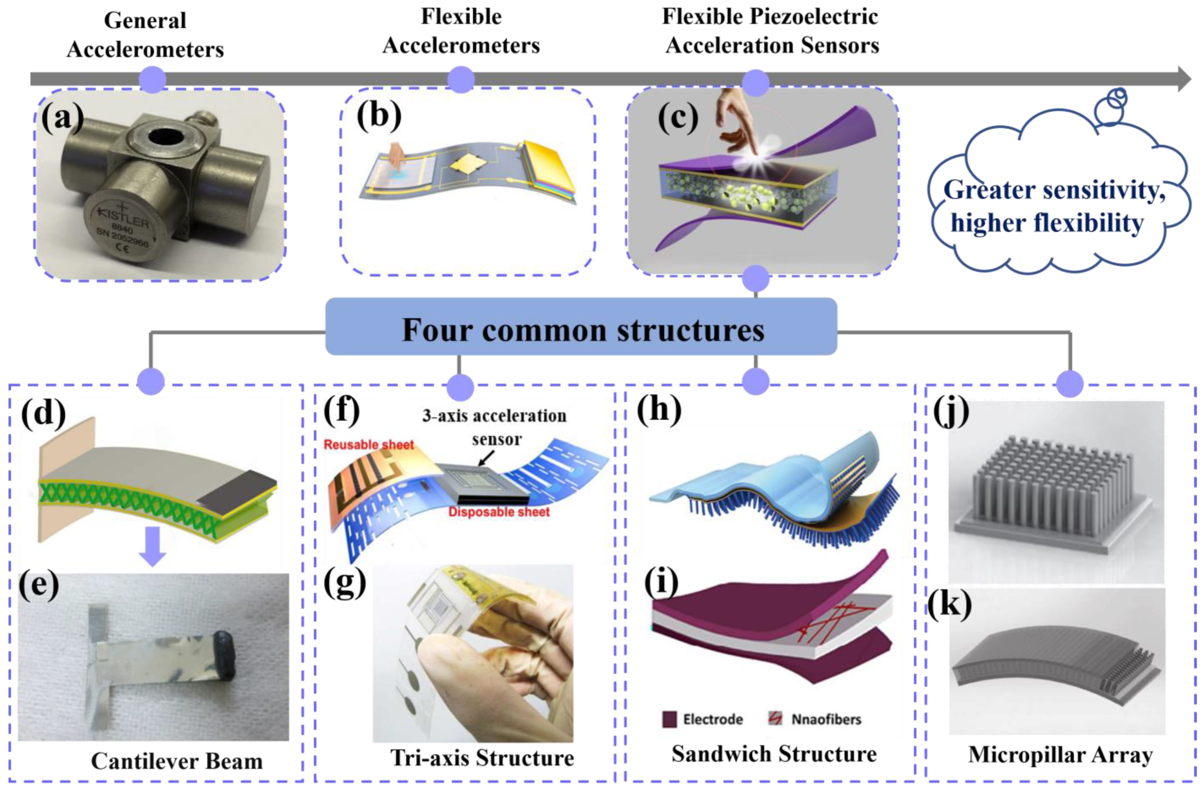
2.1. Development
2.2. Parameters
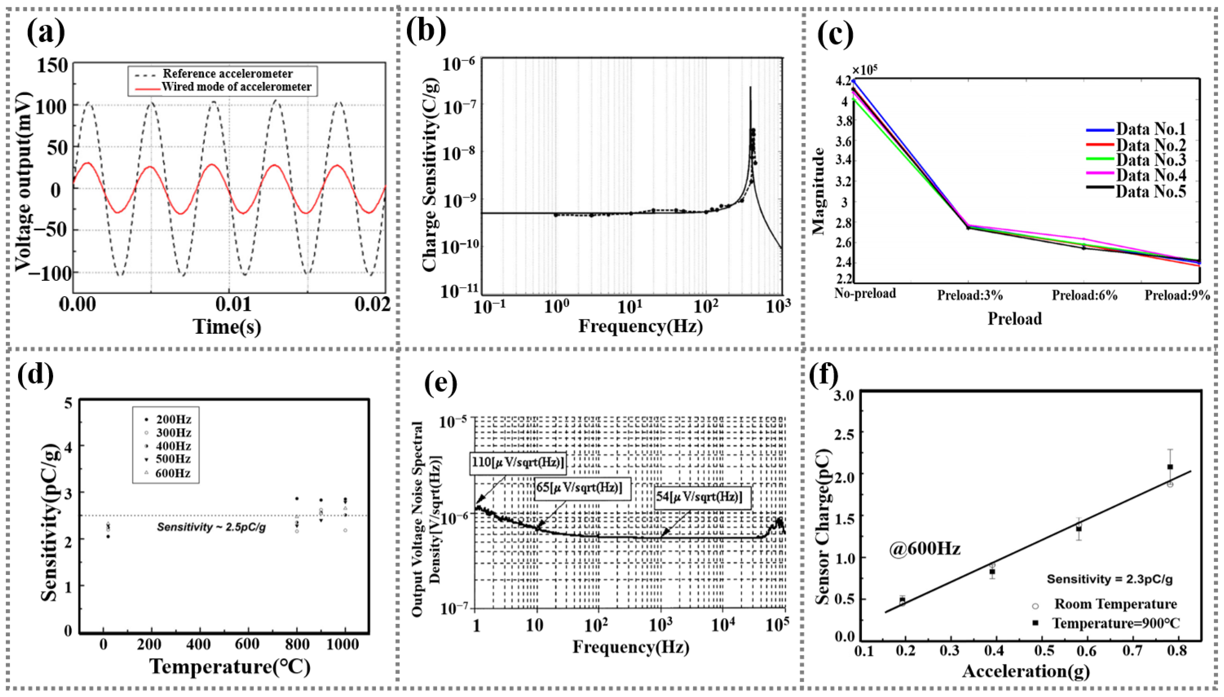
2.2.1. Frequency
2.2.2. Sensitivity
2.2.3. Pre-Tightening Torque
2.2.4. Noise
2.3. Relationship between Parameters
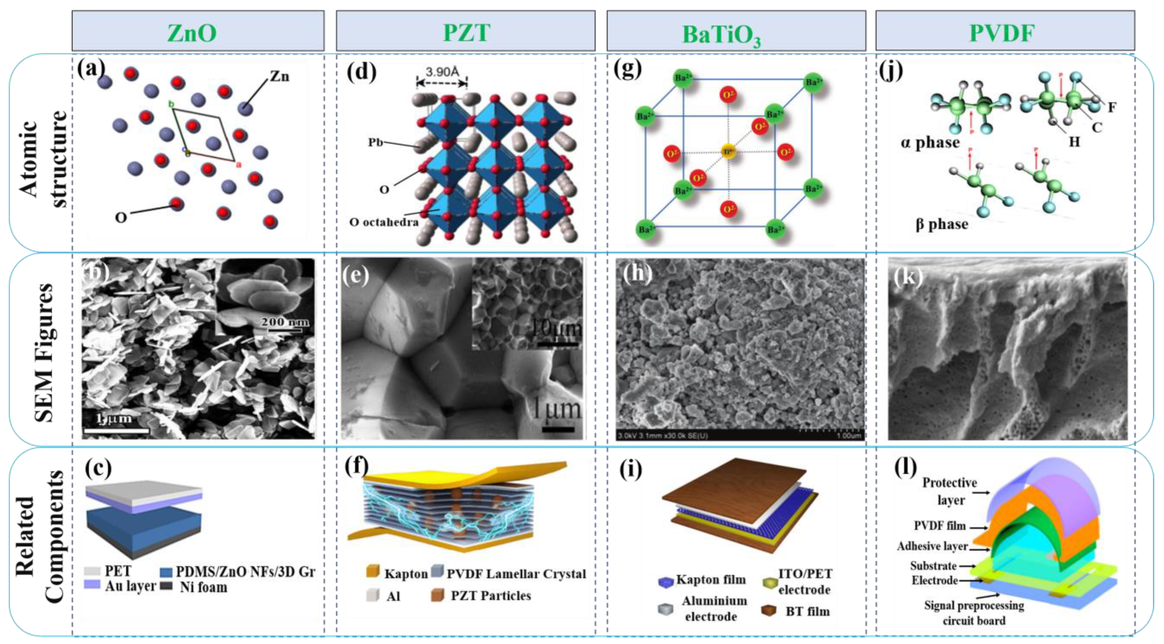
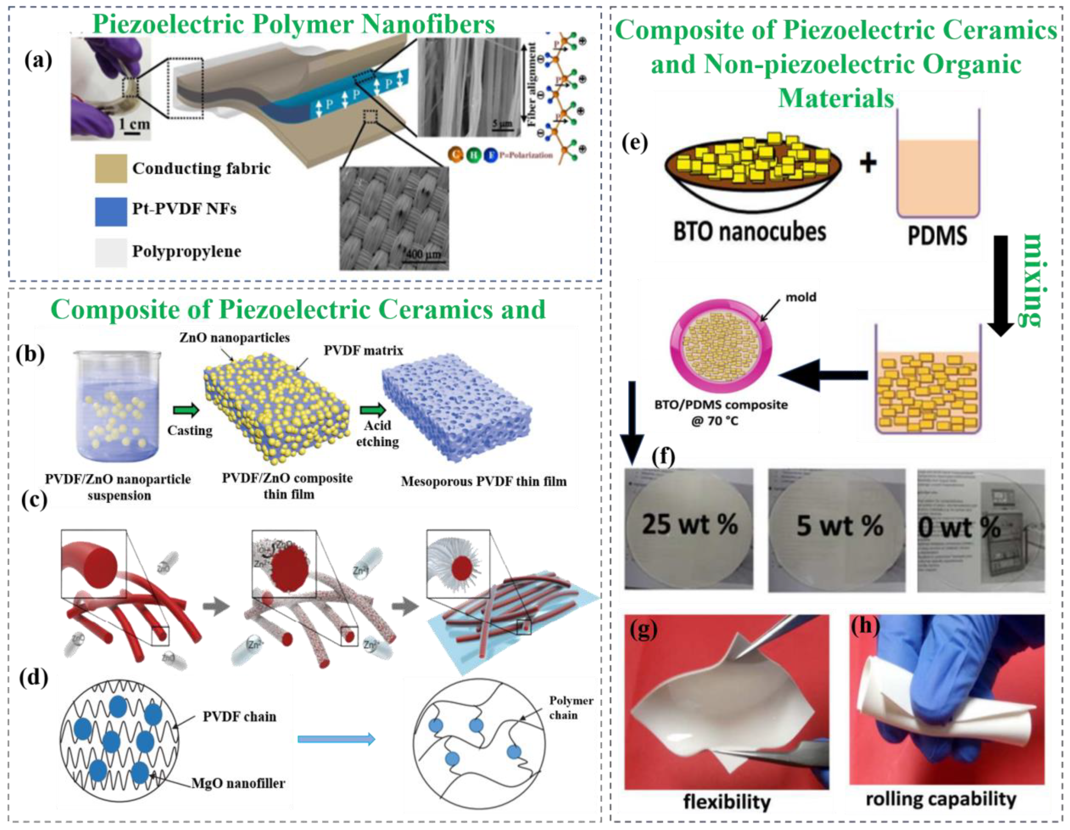
3. Materials for Flexible Piezoelectric Acceleration Sensors
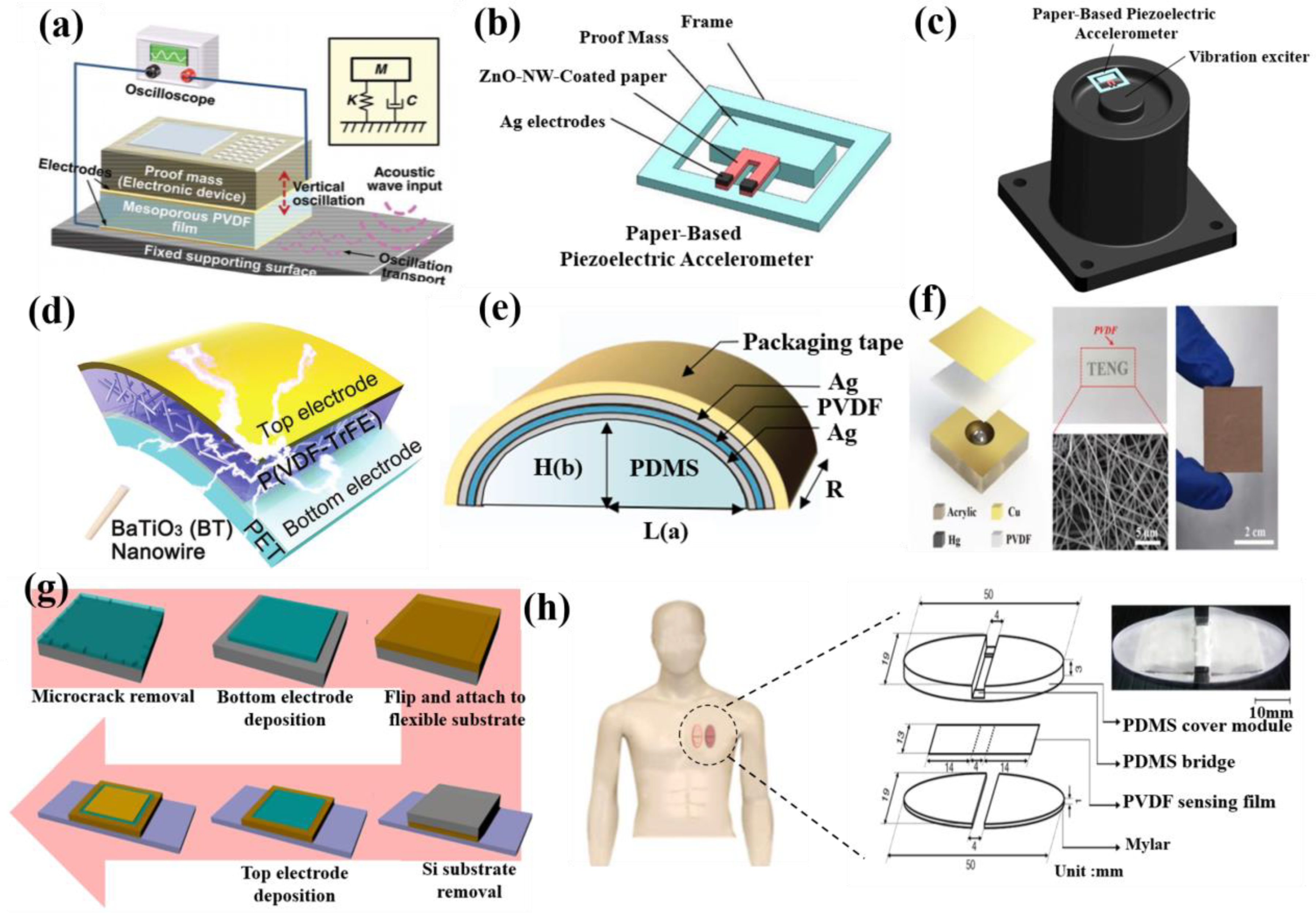
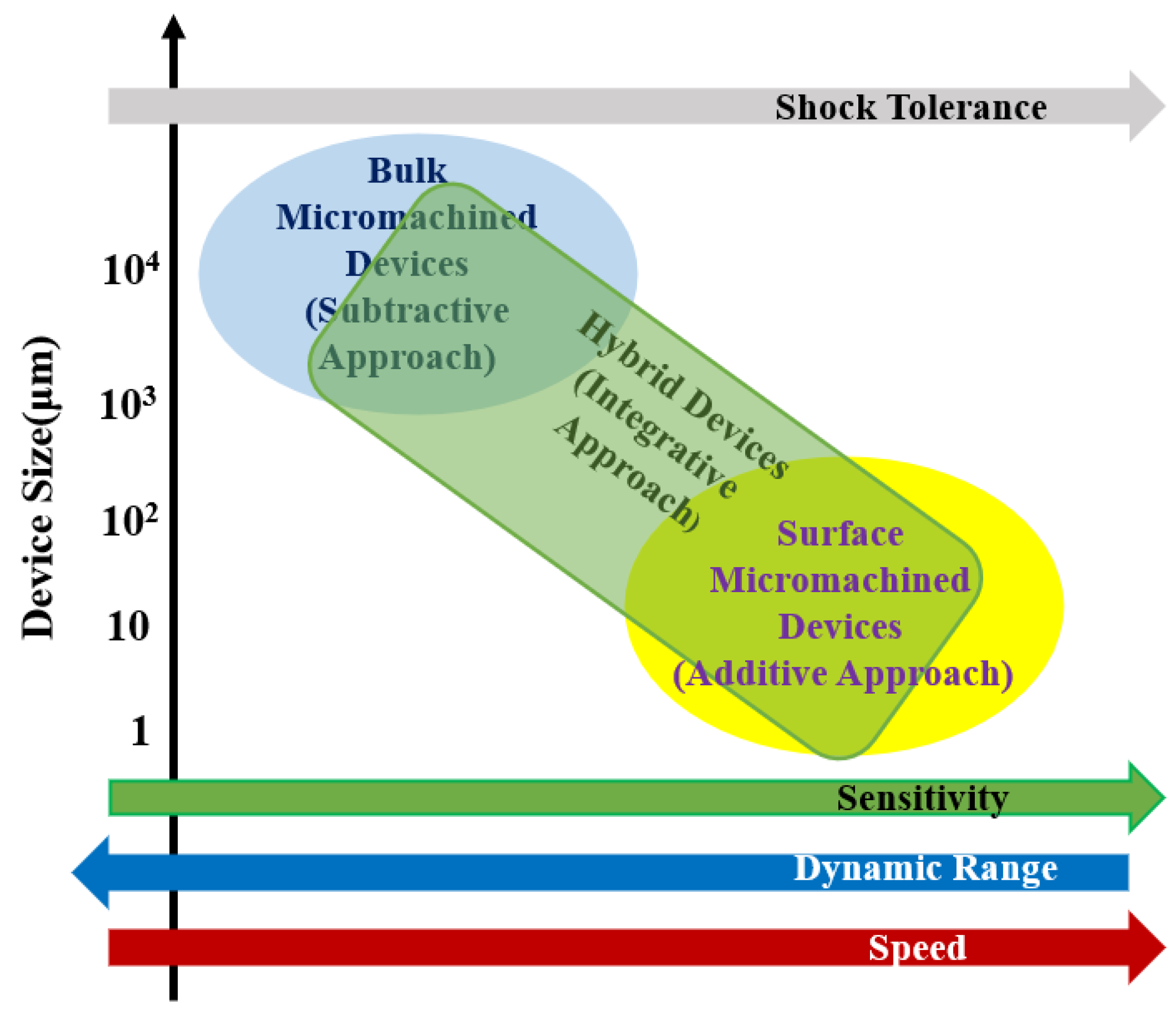
4. Structure of Flexible Piezoelectric Acceleration Sensors
5. New Technologies of Flexible Piezoelectric Acceleration Sensor
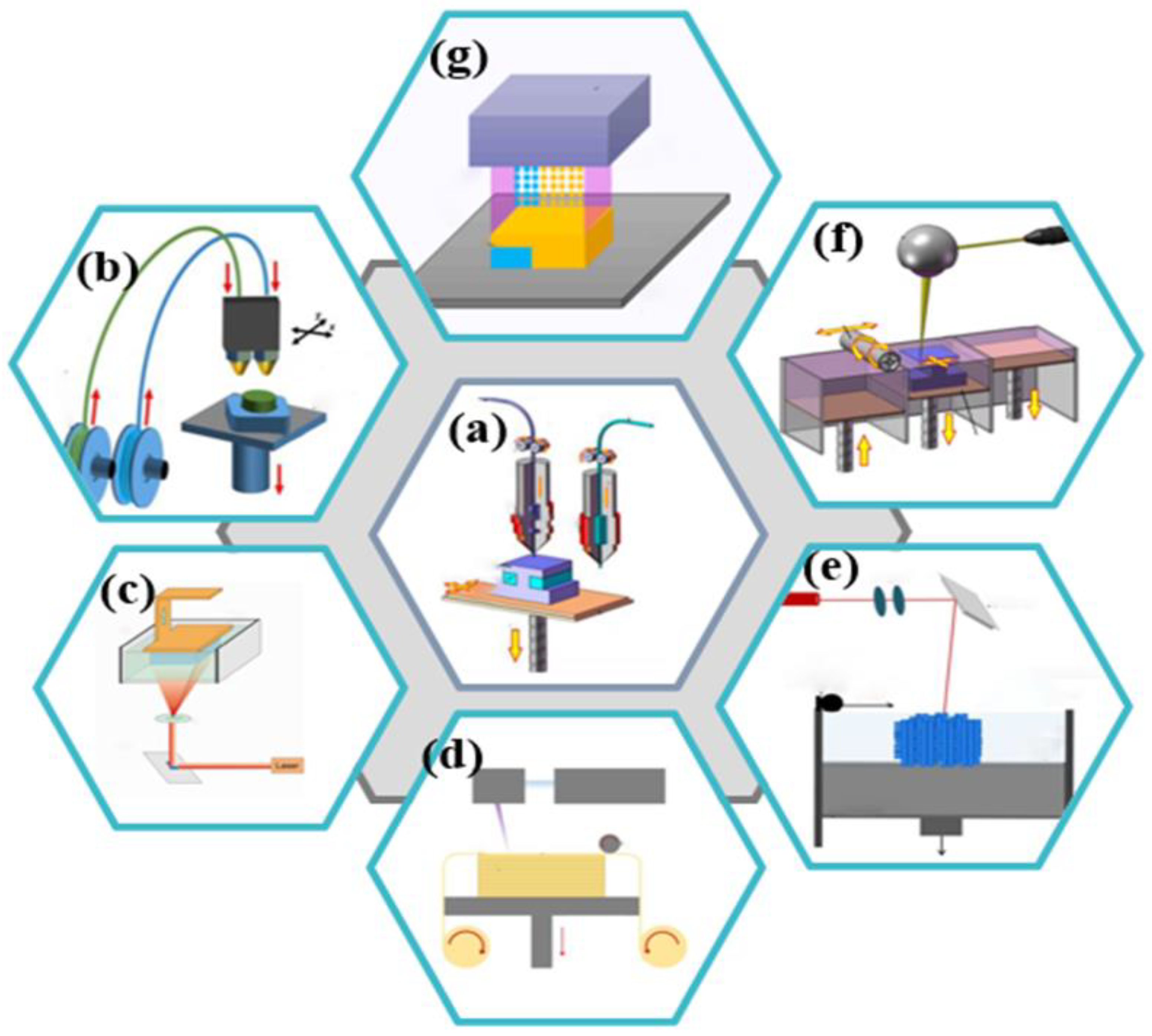
5.1. Three-Dimensional Printing Technology
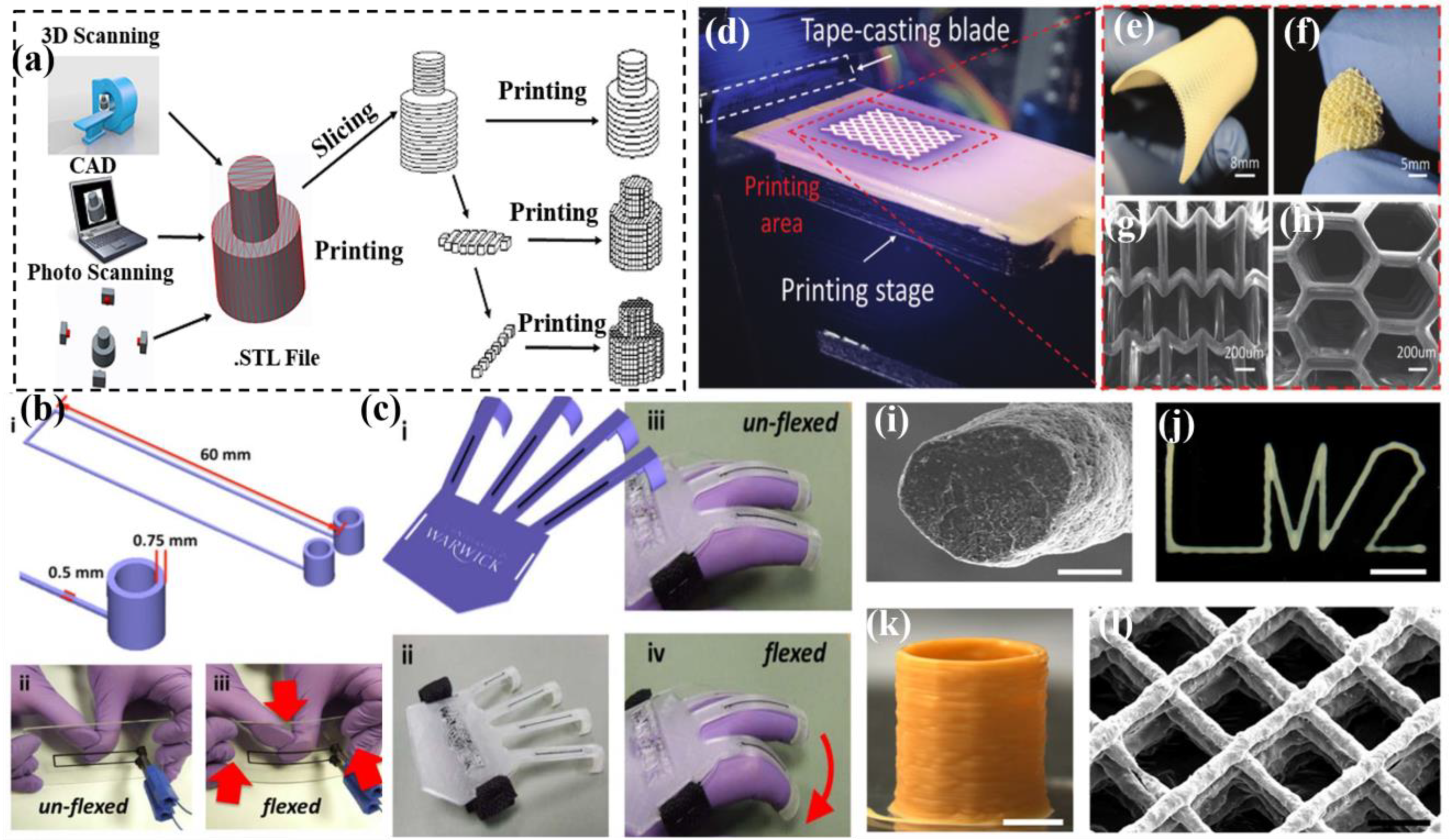
5.1.1. Introduction to 3D Printing Technology
5.1.2. Three-Dimensional Printing Technology Classification and Process Flow
- Fused Deposition Modeling (FDM)
- 2.
- Direct Ink Writing (DIW)
- 3.
- Photocuring (SLA, DLP)
- 4.
- Lamination (LOM)
- 5.
- Selective Laser Sintering and Selective Laser Melting (SLS and SLM, respectively)
- 6.
- Photopolymer Jetting (Ployjet)
- 7.
- Binder Jetting (3DP)
5.1.3. Influence of 3D Printing Parameters on Sensors
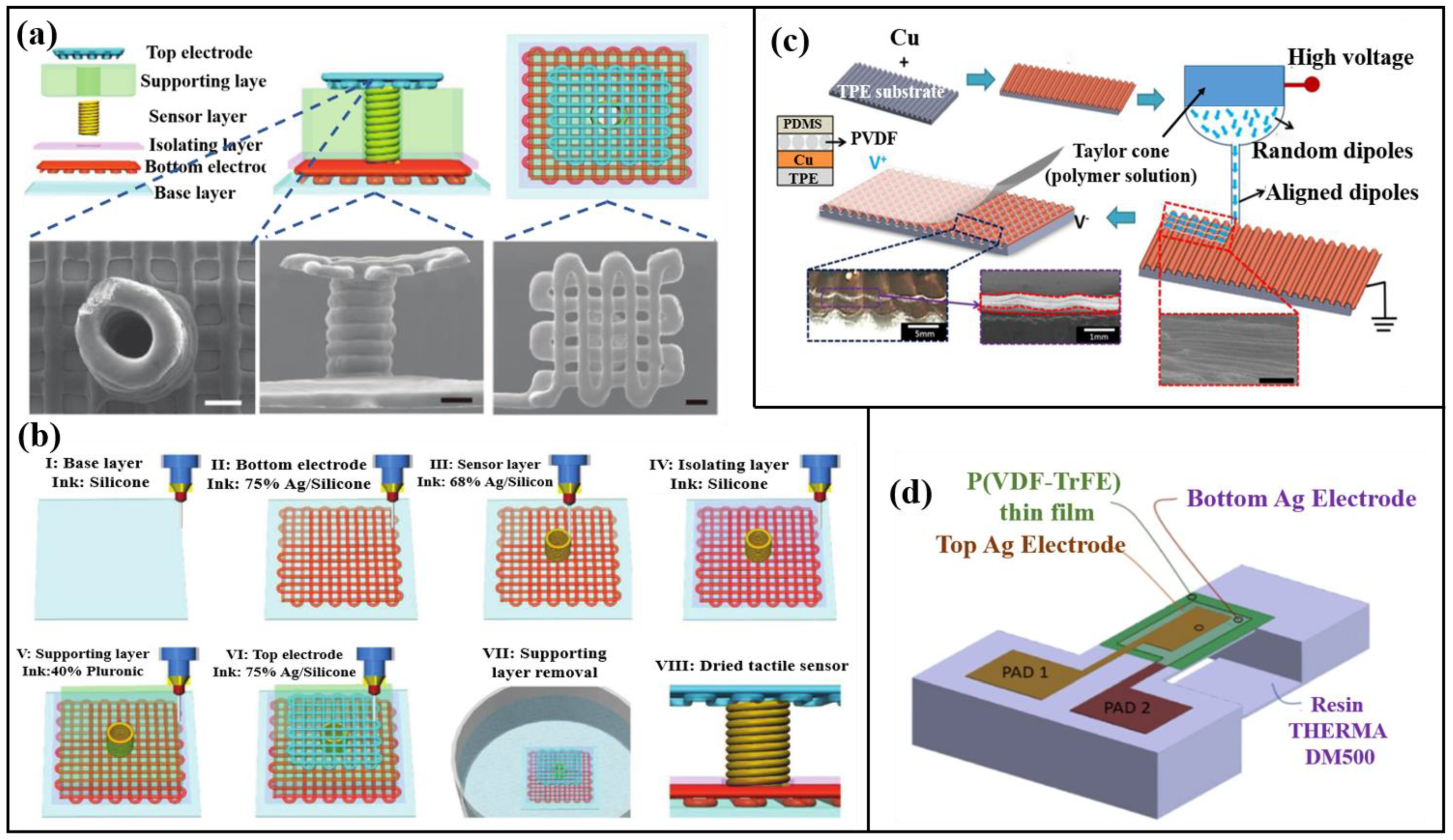
5.1.4. Application of 3D Printing Sensor
5.2. MEMS Technology
5.2.1. Introduction to MEMS Technology
5.2.2. Process of MEMS Sensors
- Addition process
- 2.
- Subtractive process
- 3.
- Integration process
- 4.
- Sensor fabrication on the silicon substrate
- 5.
- Sensor fabrication on steel substrates

5.2.3. Application of MEMS Flexible Piezoelectric Accelerometer
6. Prospect and Outlook
Author Contributions
Funding
Institutional Review Board Statement
Informed Consent Statement
Data Availability Statement
Conflicts of Interest
References
- Al-Turjman, F.; Nawaz, M.H.; Ulusar, U.D. Intelligence in the Internet of Medical Things era: A systematic review of current and future trends. Comput. Commun. 2020, 150, 644. [Google Scholar] [CrossRef]
- Yin, R.; Wang, D.; Zhao, S.; Lou, Z.; Shen, G. Wearable Sensors-Enabled Human–Machine Interaction Systems: From Design to Application. Adv. Funct. Mater. 2021, 31, 2008936. [Google Scholar] [CrossRef]
- Wang, Z.; Yang, Z.; Dong, T. A review of wearable technologies for elderly care that can accurately track indoor position, recognize physical activities and monitor vital signs in real time. Sensors 2017, 17, 341. [Google Scholar] [CrossRef] [Green Version]
- Abdulkarem, M.; Samsudin, K.; Rokhani, F.Z.; Rasid, M.F.A. Wireless sensor network for structural health monitoring: A contemporary review of technologies, challenges, and future direction. Struct. Health Monit. 2020, 19, 693. [Google Scholar] [CrossRef]
- Sunar, M.; Rao, S. Recent advances in sensing and control of flexible structures via piezoelectric materials technology. Appl. Mech. Rev. 1999, 52, 1–16. [Google Scholar] [CrossRef]
- Lu, Y. Industry 4.0: A survey on technologies, applications and open research issues. J. Ind. Inf. Integr. 2017, 6, 1–10. [Google Scholar] [CrossRef]
- Wu, J.; Guo, S.; Huang, H.; Liu, W.; Xiang, Y. Information and Communications Technologies for Sustainable Development Goals: State-of-the-Art, Needs and Perspectives. IEEE Commun. Surv. Tutor. 2018, 20, 2389. [Google Scholar] [CrossRef] [Green Version]
- Leal Filho, W.; Yang, P.; Eustachio, J.H.P.P.; Azul, A.M.; Gellers, J.C.; Gielczyk, A.; Dinis, M.A.P.; Kozlova, V. Deploying digitalisation and artificial intelligence in sustainable development research. Environ. Dev. Sustain. 2022, 25, 4957–4988. [Google Scholar] [CrossRef] [PubMed]
- Liao, Q.; Yin, Y.; Zhang, J.; Si, W.; Hou, W.; Qin, L. In Situ Growth of Nanosilver on Fabric for Flexible Stretchable Electrodes. Int. J. Mol. Sci. 2022, 23, 13236. [Google Scholar] [CrossRef] [PubMed]
- Hou, W.; Liao, Q.; Xie, S.; Song, Y.; Qin, L. Prospects and Challenges of Flexible Stretchable Electrodes for Electronics. Coatings 2022, 12, 558. [Google Scholar] [CrossRef]
- Mohankumar, P.; Ajayan, J.; Yasodharan, R.; Devendran, P.; Sambasivam, R. A review of micromachined sensors for automotive applications. Measurement 2019, 140, 305. [Google Scholar] [CrossRef]
- Ai, C.; Zhao, X.; Wen, D. Characteristics Research of a High Sensitivity Piezoelectric MOSFET Acceleration Sensor. Sensors 2020, 20, 4988. [Google Scholar] [CrossRef] [PubMed]
- Deng, W.; Yang, T.; Jin, L.; Yan, C.; Huang, H.; Chu, X.; Wang, Z.; Xiong, D.; Tian, G.; Gao, Y.; et al. Cowpea-structured PVDF/ZnO nanofibers based flexible self-powered piezoelectric bending motion sensor towards remote control of gestures. Nano Energy 2019, 55, 516. [Google Scholar] [CrossRef]
- Cui, H.; Hensleigh, R.; Yao, D.; Maurya, D.; Kumar, P.; Kang, M.G.; Priya, S.; Zheng, X. Three-dimensional printing of piezoelectric materials with designed anisotropy and directional response. Nat. Mater. 2019, 18, 234. [Google Scholar] [CrossRef]
- Pan, M.; Yuan, C.; Liang, X.; Zou, J.; Zhang, Y.; Bowen, C. Triboelectric and Piezoelectric Nanogenerators for Future Soft Robots and Machines. iScience 2020, 23, 101682. [Google Scholar] [CrossRef] [PubMed]
- Navaraj, W.; Dahiya, R. Fingerprint-enhanced capacitive-piezoelectric flexible sensing skin to discriminate static and dynamic tactile stimuli. Adv. Intell. Syst. 2019, 1, 1900051. [Google Scholar] [CrossRef]
- Park, Y.; Shim, J.; Jeong, S.; Yi, G.-R.; Chae, H.; Bae, J.W.; Kim, S.O.; Pang, C. Microtopography-Guided Conductive Patterns of Liquid-Driven Graphene Nanoplatelet Networks for Stretchable and Skin-Conformal Sensor Array. Adv. Mater. 2017, 29, 1606453. [Google Scholar] [CrossRef]
- Cao, R.; Pu, X.; Du, X.; Yang, W.; Wang, J.; Guo, H.; Zhao, S.; Yuan, Z.; Zhang, C.; Li, C. Screen-printed washable electronic textiles as self-powered touch/gesture tribo-sensors for intelligent human–machine interaction. ACS Nano 2018, 12, 5190. [Google Scholar] [CrossRef]
- Lowe, R.; Andreasson, R.; Alenljung, B.; Lund, A.; Billing, E. Designing for a Wearable Affective Interface for the NAO Robot: A Study of Emotion Conveyance by Touch. Multimodal Technol. Interact. 2018, 2, 2. [Google Scholar] [CrossRef] [Green Version]
- Han, J.H.; Min, B.K.; Hong, S.K.; Park, H.; Kwak, J.-H.; Wang, H.S.; Joe, D.J.; Park, J.H.; Jung, Y.H.; Hur, S.; et al. Machine learning-based self-powered acoustic sensor for speaker recognition. Nano Energy 2018, 53, 658–665. [Google Scholar] [CrossRef]
- Jin, L.; Ma, S.; Deng, W.; Yan, C.; Yang, T.; Chu, X.; Tian, G.; Xiong, D.; Lu, J.; Yang, W. Polarization-free high-crystallization β-PVDF piezoelectric nanogenerator toward self-powered 3D acceleration sensor. Nano Energy 2018, 50, 632. [Google Scholar] [CrossRef]
- da Fonseca, I.M.; Rade, D.A.; Goes, L.C.S.; de Paula Sales, T. Attitude and vibration control of a satellite containing flexible solar arrays by using reaction wheels, and piezoelectric transducers as sensors and actuators. Acta Astronaut. 2017, 139, 357. [Google Scholar] [CrossRef]
- Chen, X.; Zeng, Q.; Shao, J.; Li, S.; Luo, Y. Channel-Crack-Designed Suspended Sensing Membrane as a Fully Flexible Vibration Sensor with High Sensitivity and Dynamic Range. ACS Appl. Mater. Interfaces 2021, 13, 34637–34647. [Google Scholar] [CrossRef] [PubMed]
- Yuan, X.; Gao, X.; Shen, X.; Yang, J.; Dong, S. A 3D-printed, alternatively tilt-polarized PVDF-TrFE polymer with enhanced piezoelectric effect for self-powered sensor application. Nano Energy 2021, 85, 105985. [Google Scholar] [CrossRef]
- Smart Cities. Available online: https://www.freepik.com/free-vector/isometric-smart-city-background_4358963.htm (accessed on 27 February 2023).
- Smart Farming. Available online: https://www.freepik.com/free-photo/smart-robotic-farmers-concept-robot-farmers-agriculture-technology-farm-automation_21544365.htm (accessed on 27 February 2023).
- Smart Buildings. Available online: https://www.freepik.com/free-vector/isometric-smart-city-background_4358967.htm (accessed on 4 November 2022).
- Armin, D.; Jakob, R.; Gregor, E.; Miha, B. On the performance of direct piezoelectric rotational accelerometers in experimental structural dynamics. Measurement 2018, 127, 292. [Google Scholar] [CrossRef]
- Chen, X.; Luo, L.; Zeng, Z.; Jiao, J.; Shehzad, M.; Yuan, G.; Luo, H.; Wang, Y. Bio-inspired flexible vibration visualization sensor based on piezo-electrochromic effect. J. Mater. 2020, 6, 643–650. [Google Scholar] [CrossRef]
- Zheng, L.; Shuai, C.; Wang, L.; Shi, R.; Shen, G. Ultrasensitive and ultraflexible e-skins with dual functionalities for wearable electronics. Nano Energy 2017, 38, 28–35. [Google Scholar] [CrossRef]
- Tsukamoto, T.; Umino, Y.; Shiomi, S.; Yamada, K.; Suzuki, T. Bimorph piezoelectric vibration energy harvester with flexible 3D meshed-core structure for low frequency vibration. Sci. Technol. Adv. Mater. 2018, 19, 660. [Google Scholar] [CrossRef] [Green Version]
- Yamamoto, Y.; Harada, S.; Yamamoto, D.; Honda, W.; Arie, T.; Akita, S.; Takei, K. Printed multifunctional flexible device with an integrated motion sensor for health care monitoring. Sci. Adv. 2016, 2, e1601473. [Google Scholar] [CrossRef] [Green Version]
- Pang, C.; Koo, J.H.; Nguyen, A.; Caves, J.M.; Kim, M.G.; Chortos, A.; Kim, K.; Wang, P.J.; Tok, J.B.H.; Bao, Z. Highly Skin-Conformal Microhairy Sensor for Pulse Signal Amplification. Adv. Mater. 2015, 27, 634–640. [Google Scholar] [CrossRef]
- Wu, Y.; Ma, Y.; Zheng, H.; Ramakrishna, S. Piezoelectric materials for flexible and wearable electronics: A review. Mater. Des. 2021, 211, 110164. [Google Scholar] [CrossRef]
- Chen, X.; Li, X.; Shao, J.; An, N.; Tian, H.; Wang, C.; Han, T.; Wang, L.; Lu, B. High-Performance Piezoelectric Nanogenerators with Imprinted P(VDF-TrFE)/BaTiO3 Nanocomposite Micropillars for Self-Powered Flexible Sensors. Small 2017, 13, 1604245. [Google Scholar] [CrossRef] [PubMed]
- Huang, Y.; Fan, X.; Chen, S.C.; Zhao, N. Emerging Technologies of Flexible Pressure Sensors: Materials, Modeling, Devices, and Manufacturing. Adv. Funct. Mater. 2019, 29, 1808509. [Google Scholar] [CrossRef]
- Bergmayr, T.; Kralovec, C.; Schagerl, M. Vibration-Based Thermal Health Monitoring for Face Layer Debonding Detection in Aerospace Sandwich Structures. Appl. Sci. 2020, 11, 211. [Google Scholar] [CrossRef]
- Zhang, S.; Chen, Z.; Li, G.; Wu, Y. A novel Z-shaped elastic flange structure for increasing the amplitude output of a piezoelectric ultrasonic transducer. Sens. Actuators A Phys. 2021, 331, 112995. [Google Scholar] [CrossRef]
- Pan, Q.S.; He, L.G.; Pan, C.L.; Xiao, G.J.; Feng, Z.H. Resonant-type inertia linear motor based on the harmonic vibration synthesis of piezoelectric bending actuator. Sens. Actuators A Phys. 2014, 209, 169. [Google Scholar] [CrossRef]
- Levinzon, F.A. Noise of piezoelectric accelerometer with integral FET amplifier. IEEE Sens. J. 2005, 5, 1235. [Google Scholar] [CrossRef]
- Gesing, A.L.; Alves, F.D.P.; Paul, S.; Cordioli, J.A. On the design of a MEMS piezoelectric accelerometer coupled to the middle ear as an implantable sensor for hearing devices. Sci. Rep. 2018, 8, 3920. [Google Scholar] [CrossRef] [Green Version]
- Li, W.; Weldon, J.A.; Huang, Y.; Wang, K. Design and Simulation of Piezoelectric-Charge-Gated Thin-Film Transistor for Tactile Sensing. IEEE Electron Device Lett. 2016, 37, 325. [Google Scholar] [CrossRef]
- Guo, Z.Q.; Liu, L.Y.; Liu, J.; Wu, N.J. Noise analysis for high speed CMOS image sensor. Sel. Pap. Conf. Photoelectron. Technol. Comm. Chin. Soc. Astronaut. 2015, 9522, 182–187. [Google Scholar] [CrossRef]
- Shen, Z.; Tan, C.Y.; Yao, K.; Zhang, L.; Chen, Y.F. A miniaturized wireless accelerometer with micromachined piezoelectric sensing element. Sens. Actuators A Phys. 2016, 241, 113. [Google Scholar] [CrossRef]
- Kollias, A.T.; Avaritsiotis, J.N. A study on the performance of bending mode piezoelectric accelerometers. Sens. Actuators A Phys. 2005, 121, 434. [Google Scholar] [CrossRef]
- Feng, G.H.; Pan, Y.L. Establishing a cost-effective sensing system and signal processing method to diagnose preload levels of ball screws. Mech. Syst. Signal Process. 2012, 28, 78. [Google Scholar] [CrossRef]
- Jiang, C.; Liu, X.; Yu, F.P.; Zhang, S.; Zhao, X. High-temperature vibration sensor based on Ba2TiSi2O8 piezoelectric crystal with ultra-stable sensing performance up to 650 °C. IEEE Trans. Ind. Electron. 2020, 68, 12850–12859. [Google Scholar] [CrossRef]
- Zhang, S.; Jiang, X.; Lapsley, M.; Moses, P.; Shrout, T.R. Piezoelectric Accelerometers for Ultrahigh Temperature Application. Appl. Phys. Lett. 2010, 96, 013506. [Google Scholar] [CrossRef]
- Bochobza-Degani, O.; Dan, J.S.; Socher, E.; Nemirovsky, Y. Design and noise consideration of an accelerometer employing modulated integrative differential optical sensing. Sens. Actuators A Phys. 2000, 84, 53. [Google Scholar] [CrossRef]
- Yaghootkar, B.; Azimi, S.; Bahreyni, B. A High-Performance Piezoelectric Vibration Sensor. IEEE Sens. J. 2017, 17, 4005. [Google Scholar] [CrossRef]
- Yan, L.; Zhao, Y.; Wang, W.; Lu, S.; Jiang, Z. A high-performance multi-beam microaccelerometer for vibration monitoring in intelligent manufacturing equipment. Sens. Actuators A Phys. 2013, 189, 8–16. [Google Scholar] [CrossRef]
- Roy, A.L.; Sarkar, H.; Dutta, A.; Bhattacharyya, T.K. A high precision SOI MEMS–CMOS ±4 g piezoresistive accelerometer. Sens. Actuators A Phys. 2014, 210, 77. [Google Scholar] [CrossRef]
- Speller, K.E.; Yu, D. A low-noise MEMS accelerometer for unattended ground sensor applications. In Unattended/Unmanned Ground, Ocean, and Air Sensor Technologies and Applications; SPIE: Bellingham, WA, USA, 2004; Volume 5417, pp. 63–72. [Google Scholar] [CrossRef]
- Wang, L.P.; Deng, K.; Zou, L.; Wolf, R.; Davis, R.J.; Trolier-Mckinstry, S. Microelectromechanical systems (MEMS) accelerometers using lead zirconate titanate thick films. Electron Device Lett. IEEE 2002, 23, 182. [Google Scholar] [CrossRef]
- Gerfers, F.; Kohlstadt, M.; Bar, H.; He, M.Y.; Wang, L.P. Sub-μg ultra-low-noise MEMS accelerometers based on CMOS-compatible piezoelectric AlN thin films. In Proceedings of the TRANSDUCERS 2007-2007 International Solid-State Sensors, Actuators and Microsystems Conference, Lyon, France, 10–14 June 2007; pp. 1191–1194. [Google Scholar] [CrossRef]
- PCB Piezotronics MTS Systems Corp. Available online: https://www.pcb.com/products?m=357B69 (accessed on 21 February 2023).
- Shi, J.; Liu, S.; Zhang, L.; Yang, B.; Shu, L.; Yang, Y.; Ren, M.; Wang, Y.; Chen, J.; Chen, W. Smart Textile-Integrated Microelectronic Systems for Wearable Applications. Adv. Mater. 2020, 32, 1901958. [Google Scholar] [CrossRef] [PubMed]
- Liao, Q.; Hou, W.; Liao, K.; Chen, L.; Song, Y.; Gao, G.; Qin, L. Solid-phase sintering and vapor-liquid-solid growth of BP@MgO quantum dot crystals with a high piezoelectric response. J. Adv. Ceram. 2022, 11, 1725. [Google Scholar] [CrossRef]
- Hofmann, P.; Walch, A.; Dinkelmann, A.; Selvarayan, S.K.; Gresser, G.T. Woven piezoelectric sensors as part of the textile reinforcement of fiber reinforced plastics. Compos. Part A Appl. Sci. Manuf. 2019, 116, 79. [Google Scholar] [CrossRef]
- Mahdavi, Z.; Khodakarami, M.I.; Kontoni, D.-P. Qualitative flaw detection in piezoelectric material for elastostatics using linear sampling method. In Proceedings of the 6th IC-EpsMsO, Athens, Greece, 8–11 July 2015. [Google Scholar]
- Stoynov, Y.; Rangelov, T. Inverse Scattering Problems for Cracked Piezoelectric Media. Aip Conf. Am. Inst. Phys. 2013, 1561, 318–326. [Google Scholar] [CrossRef]
- Valagiannopoulos, C. On measuring the permittivity tensor of an anisotropic material from the transmission coefficients. Prog. Electromagn. Res. B 2008, 9, 105. [Google Scholar] [CrossRef] [Green Version]
- Valagiannopoulos, C.A.; Tsitsas, N.L. Integral equation analysis of a low-profile receiving planar microstrip antenna with a cloaking superstrate. Radio Sci. 2012, 47, 1–12. [Google Scholar] [CrossRef]
- Boryło, P.; Matus, K.; Lukaszkowicz, K.; Kubacki, J.; Balin, K.; Basiaga, M.; Szindler, M.; Mikuła, J. The influence of atomic layer deposition process temperature on ZnO thin film structure. Appl. Surf. Sci. 2019, 474, 177. [Google Scholar] [CrossRef]
- Han, X.G.; He, H.Z.; Kuang, Q.; Zhou, X.; Zhang, X.H.; Xu, T.; Xie, Z.X.; Zheng, L.S. Controlling Morphologies and Tuning the Related Properties of Nano/Microstructured ZnO Crystallites. J. Phys. Chem. C 2009, 113, 584. [Google Scholar] [CrossRef]
- Qian, Y.K.; Kang, D.J. Poly(dimethylsiloxane)/ZnO Nanoflakes/Three-Dimensional Graphene Heterostructures for High-Performance Flexible Energy Harvesters with Simultaneous Piezoelectric and Triboelectric Generation. ACS Appl. Mater. Interfaces 2018, 10, 32281–32288. [Google Scholar] [CrossRef]
- Jin, W.; Durussel, A.; Sandu, C.S.; Sahini, M.G.; He, Z.; Setter, N. Mechanism of hydrothermal growth of ferroelectric PZT nanowires. J. Cryst. Growth 2012, 347, 1–6. [Google Scholar] [CrossRef]
- Shin, D.-J.; Jeong, S.-J.; Seo, C.-E.; Cho, K.-H.; Koh, J.-H. Multi-layered piezoelectric energy harvesters based on PZT ceramic actuators. Ceram. Int. 2015, 41, S686. [Google Scholar] [CrossRef]
- Tian, G.; Deng, W.; Gao, Y.; Xiong, D.; Yan, C.; He, X.; Yang, T.; Jin, L.; Chu, X.; Zhang, H.; et al. Rich lamellar crystal baklava-structured PZT/PVDF piezoelectric sensor toward individual table tennis training. Nano Energy 2019, 59, 574. [Google Scholar] [CrossRef]
- Sood, A.; Desseigne, M.; Dev, A.; Maurizi, L.; Kumar, A.; Millot, N.; Han, S.S. A Comprehensive Review on Barium Titanate Nanoparticles as a Persuasive Piezoelectric Material for Biomedical Applications: Prospects and Challenges. Small 2023, 19, 2206401. [Google Scholar] [CrossRef]
- Upadhyay, S.; Shrivastava, J.; Solanki, A.; Choudhary, S.; Sharma, V.; Kumar, P.; Singh, N.; Satsangi, V.R.; Shrivastav, R.; Waghmare, U.V.; et al. Enhanced Photoelectrochemical Response of BaTiO3 with Fe Doping: Experiments and First-Principles Analysis. J. Phys. Chem. C 2011, 115, 24373–24380. [Google Scholar] [CrossRef]
- Selvarajan, S.; Alluri, N.R.; Chandrasekhar, A.; Kim, S.J. Unconventional active biosensor made of piezoelectric BaTiO3 nanoparticles for biomolecule detection. Sens. Actuators B Chem. 2017, 253, 1180–1187. [Google Scholar] [CrossRef]
- Sharma, T.; Je, S.S.; Gill, B.; Zhang, J. Patterning piezoelectric thin film PVDF–TrFE based pressure sensor for catheter application. Sens. Actuators A Phys. 2012, 177, 87. [Google Scholar] [CrossRef]
- Rajabi, H.; Ghaemi, N.; Madaeni, S.S.; Daraei, P.; Khadivi, M.A.; Falsafi, M. Nanoclay embedded mixed matrix PVDF nanocomposite membrane: Preparation, characterization and biofouling resistance. Appl. Surf. Sci. 2014, 313, 207. [Google Scholar] [CrossRef]
- Kalimuldina, G.; Turdakyn, N.; Abay, I.; Medeubayev, A.; Nurpeissova, A.; Adair, D.; Bakenov, Z. A Review of Piezoelectric PVDF Film by Electrospinning and Its Applications. Sensors 2020, 20, 5214. [Google Scholar] [CrossRef]
- Duan, S.; Wu, J.; Xia, J.; Lei, W. Innovation Strategy Selection Facilitates High-Performance Flexible Piezoelectric Sensors. Sensors 2020, 20, 2820. [Google Scholar] [CrossRef]
- Ghosh, S.K.; Mandal, D. Synergistically enhanced piezoelectric output in highly aligned 1D polymer nanofibers integrated all-fiber nanogenerator for wearable nano-tactile sensor. Nano Energy 2018, 53, 245–257. [Google Scholar] [CrossRef]
- Meng, X.; Zhang, Z.; Lin, D.; Liu, W.; Zhou, S.; Ge, S.; Su, Y.; Peng, C.; Zhang, L. Effects of particle size of dielectric fillers on the output performance of piezoelectric and triboelectric nanogenerators. J. Adv. Ceram. 2021, 10, 991. [Google Scholar] [CrossRef]
- Qi, Y.; Pan, L.; Ma, L.; Liao, P.; Ge, J.; Zhang, D.; Zheng, Q.; Yu, B.; Tang, Y.; Sun, D. Investigation on FT-IR spectra and dielectric property of PVDF/inorganic composites. J. Mater. Sci. Mater. Electron. 2013, 24, 1446. [Google Scholar] [CrossRef]
- Newnham, R.E.; Skinner, D.P.; Cross, L.E. Connectivity and Piezoelectric–Pyroelectric Composite. Mater. Res. Bull. 1978, 13, 525. [Google Scholar] [CrossRef]
- Garg, T.; Annapureddy, V.; Sekhar, K.C.; Jeong, D.Y.; Dabra, N.; Hundal, J.S. Modulation in polymer properties in PVDF/BCZT composites with ceramic content and their energy density capabilities. Polym. Compos. 2020, 41, 5305–5316. [Google Scholar] [CrossRef]
- Zhen, L.; Lu, L.; Yao, Y.; Liu, J.; Yang, B. Flexible inorganic piezoelectric functional films and their applications. J. Adv. Ceram. 2023, 12, 433. [Google Scholar] [CrossRef]
- Mao, Y.; Zhao, P.; Mcconohy, G.; Yang, H.; Tong, Y.; Wang, X. Sponge-Like Piezoelectric Polymer Films for Scalable and Integratable Nanogenerators and Self-Powered Electronic Systems. Adv. Energy Mater. 2014, 4, 1301624. [Google Scholar] [CrossRef]
- Yang, T.; Pan, H.; Tian, G.; Zhang, B.; Yang, W. Hierarchically Structured PVDF/ZnO Core-shell Nanofibers for Self-powered Physiological Monitoring Electronics. Nano Energy 2020, 72, 104706. [Google Scholar] [CrossRef]
- Arshad, A.N.; Wahid, M.; Rusop, M.; Majid, W.; Subban, R.; Rozana, M. Dielectric and Structural Properties of Poly(vinylidene fluoride) (PVDF) and Poly(vinylidene fluoride-trifluoroethylene) (PVDF-TrFE) Filled with Magnesium Oxide Nanofillers. J. Nanomater. 2019, 2019, 5961563. [Google Scholar] [CrossRef]
- Alluri, N.R.; Chandrasekhar, A.; Vivekananthan, V.; Purusothaman, Y.; Selvarajan, S.; Jeong, J.H.; Kim, S.-J. Scavenging Biomechanical Energy Using High-Performance, Flexible BaTiO3 Nanocube/PDMS Composite Films. ACS Sustain. Chem. Eng. 2017, 5, 4730. [Google Scholar] [CrossRef]
- Liao, Q.; Hou, W.; Zhang, J.; Qin, L. Controllable Preparation of Silver Nanowires and Its Application in Flexible Stretchable Electrode. Coatings 2022, 12, 1756. [Google Scholar] [CrossRef]
- Wolf, M.P.; Salieb-Beugelaar, G.B.; Patrick, H. PDMS with designer functionalities—Properties, modifications strategies, and applications. Prog. Polym. Sci. 2018, 83, 97. [Google Scholar] [CrossRef]
- Li, Z.; Peng, Y.; Xu, Z.; Peng, J.; Pu, H. Harnessing energy from suspension systems of oceanic vehicles with high-performance piezoelectric generators. Energy 2021, 228, 120523. [Google Scholar] [CrossRef]
- Chen, Y.; Xue, X. Advances in the Structural Health Monitoring of Bridges Using Piezoelectric Transducers. Sensors 2018, 18, 4312. [Google Scholar] [CrossRef] [Green Version]
- Jiang, X.; Kim, K.; Zhang, S.; Johnson, J.; Salazar, G. High-Temperature Piezoelectric Sensing. Sensors 2014, 14, 144. [Google Scholar] [CrossRef] [PubMed] [Green Version]
- Wang, Y.; Song, P.; Li, X.; Ru, C.; Ferrari, G.; Balasubramanian, P.; Amabili, M.; Sun, Y.; Liu, X. A Paper-Based Piezoelectric Accelerometer. Micromachines 2018, 9, 19. [Google Scholar] [CrossRef] [Green Version]
- Jeong, C.K.; Baek, C.; Kingon, A.I.; Park, K.-I.; Kim, S.-H. Lead-Free Perovskite Nanowire-Employed Piezopolymer for Highly Efficient Flexible Nanocomposite Energy Harvester. Small 2018, 14, 1704022. [Google Scholar] [CrossRef]
- Yuan, Y.; Chen, H.; Xu, H.; Jin, Y.; Chen, G.; Zheng, W.; Wang, W.; Wang, Y.; Gao, L. Highly sensitive and wearable bionic piezoelectric sensor for human respiratory monitoring. Sens. Actuators A Phys. 2022, 345, 113818. [Google Scholar] [CrossRef]
- Zhang, B.; Zhang, L.; Deng, W.; Jin, L.; Chun, F.; Pan, H.; Gu, B.; Zhang, H.; Lv, Z.; Yang, W.; et al. Self-Powered Acceleration Sensor Based on Liquid Metal Triboelectric Nanogenerator for Vibration Monitoring. ACS Nano 2017, 11, 7440. [Google Scholar] [CrossRef]
- Chen, J.; Oh, S.K.; Nabulsi, N.; Johnson, H.; Wang, W.; Ryou, J.-H. Biocompatible and sustainable power supply for self-powered wearable and implantable electronics using III-nitride thin-film-based flexible piezoelectric generator. Nano Energy 2019, 57, 670. [Google Scholar] [CrossRef]
- Chiu, Y.; Lin, W.; Wang, H.; Huang, S.; Wu, M. Development of a piezoelectric polyvinylidene fluoride (PVDF) polymer-based sensor patch for simultaneous heartbeat and respiration monitoring. Sens. Actuators A Phys. 2013, 189, 328. [Google Scholar] [CrossRef]
- MacDonald, E.; Wicker, R. Multiprocess 3D printing for increasing component functionality. Science 2016, 353, aaf2093. [Google Scholar] [CrossRef] [PubMed]
- Kalkal, A.; Kumar, S.; Kumar, P.; Pradhan, R.; Willander, M.; Packirisamy, G.; Kumar, S.; Malhotra, B.D. Recent advances in 3D printing technologies for wearable (bio)sensors. Addit. Manuf. 2021, 46, 102088. [Google Scholar] [CrossRef]
- Park, S.; Shou, W.; Makatura, L.; Matusik, W.; Fu, K. 3D printing of polymer composites: Materials, processes, and applications. Matter 2022, 5, 43. [Google Scholar] [CrossRef]
- Xu, Y.; Wu, X.; Guo, X.; Kong, B.; Zhang, M.; Qian, X.; Mi, S.; Sun, W. The Boom in 3D-Printed Sensor Technology. Sensors 2017, 17, 1166. [Google Scholar] [CrossRef] [PubMed]
- Leigh, S.J.; Bradley, R.J.; Purssell, C.P.; Billson, D.R.; Hutchins, D.A. A Simple, Low-Cost Conductive Composite Material for 3D Printing of Electronic Sensors. PLoS ONE 2012, 7, e49365. [Google Scholar] [CrossRef]
- Yao, D.; Cui, H.; Hensleigh, R.; Smith, P.; Alford, S.; Bernero, D.; Bush, S.; Mann, K.; Wu, H.F.; Chin-Nieh, M.; et al. Achieving the Upper Bound of Piezoelectric Response in Tunable, Wearable 3D Printed Nanocomposites. Adv. Funct. Mater. 2019, 29, 1903866. [Google Scholar] [CrossRef]
- Bodkhe, S.; Turcot, G.; Gosselin, F.P.; Therriault, D. One-Step Solvent Evaporation-Assisted 3D Printing of Piezoelectric PVDF Nanocomposite Structures. ACS Appl. Mater. Interfaces 2017, 9, 20833. [Google Scholar] [CrossRef]
- Hull, C.W. Apparatus for Production of Three-Dimensional Objects by Stereolithography. U.S. Patent 638905, 8 August 1984. [Google Scholar]
- Zhang, F.; Wei, M.; Viswanathan, V.V.; Swart, B.; Shao, Y.; Wu, G.; Zhou, C. 3D printing technologies for electrochemical energy storage. Nano Energy 2017, 40, 418. [Google Scholar] [CrossRef]
- Kim, H.; Torres, F.; Wu, Y.; Villagran, D.; Lin, Y.; Tseng, T.-L. Integrated 3D printing and corona poling process of PVDF piezoelectric films for pressure sensor application. Smart Mater. Struct. 2017, 26, 085027. [Google Scholar] [CrossRef]
- Kim, H.; Torres, F.; Islam, M.T.; Islam, M.D.; Chavez, L.A.; Garcia Rosales, C.A.; Wilburn, B.R.; Stewart, C.M.; Noveron, J.C.; Tseng, T.-L.B.; et al. Increased piezoelectric response in functional nanocomposites through multiwall carbon nanotube interface and fused-deposition modeling three-dimensional printing. MRS Commun. 2017, 7, 960. [Google Scholar] [CrossRef] [Green Version]
- Muñoz, J.; Pumera, M. 3D-printed biosensors for electrochemical and optical applications. TrAC Trends Anal. Chem. 2020, 128, 115933. [Google Scholar] [CrossRef]
- Renteria, A.; Balcorta, V.H.; Marquez, C.; Rodriguez, A.A.; Renteria-Marquez, I.; Regis, J.; Wilburn, B.; Patterson, S.; Espalin, D.; Tseng, T.-L.; et al. Direct ink write multi-material printing of PDMS-BTO composites with MWCNT electrodes for flexible force sensors. Flex. Print. Electron. 2022, 7, 015001. [Google Scholar] [CrossRef]
- Bogue, R. 3D printing: The dawn of a new era in manufacturing? Assem. Autom. 2013, 33, 307. [Google Scholar] [CrossRef]
- Gross, B.C.; Erkal, J.L.; Lockwood, S.Y.; Chen, C.; Spence, D.M. Evaluation of 3D Printing and Its Potential Impact on Biotechnology and the Chemical Sciences. Anal. Chem. 2014, 86, 3240. [Google Scholar] [CrossRef]
- Tiller, B.; Reid, A.; Zhu, B.; Guerreiro, J.; Domingo-Roca, R.; Curt Jackson, J.; Windmill, J.F.C. Piezoelectric microphone via a digital light processing 3D printing process. Mater. Des. 2019, 165, 107593. [Google Scholar] [CrossRef]
- He, Y.; Wu, Y.; Fu, J.; Gao, Q.; Qiu, J. Developments of 3D Printing Microfluidics and Applications in Chemistry and Biology: A Review. Electroanalysis 2016, 28, 1658. [Google Scholar] [CrossRef]
- Fang, C.; Fang, Z. Application of 3D Printing Technology in Hepato-Biliary-Pancreatic Surgery. In Biliary Tract Surgery; Fang, C., Lau, W.Y., Eds.; Springer: Singapore, 2021; pp. 117–130. [Google Scholar] [CrossRef]
- Dutta, D.; Prinz, F.B.; Rosen, D.; Weiss, L. Layered Manufacturing: Current Status and Future Trends. J. Comput. Inf. Sci. Eng. 2000, 1, 60. [Google Scholar] [CrossRef] [Green Version]
- Ko, S.H.; Pan, H.; Grigoropoulos, C.P.; Luscombe, C.K.; Fréchet, J.M.J.; Poulikakos, D. All-inkjet-printed flexible electronics fabrication on a polymer substrate by low-temperature high-resolution selective laser sintering of metal nanoparticles. Nanotechnology 2007, 18, 345202. [Google Scholar] [CrossRef]
- Nadgorny, M.; Ameli, A. Functional Polymers and Nanocomposites for 3D Printing of Smart Structures and Devices. ACS Appl. Mater. Interfaces 2018, 10, 17489–17507. [Google Scholar] [CrossRef]
- Song, S.; Li, Y.; Wang, Q.; Zhang, C. Boosting piezoelectric performance with a new selective laser sintering 3D printable PVDF/graphene nanocomposite. Compos. Part A Appl. Sci. Manuf. 2021, 147, 106452. [Google Scholar] [CrossRef]
- Pugalendhi, A.; Ranganathan, R. A review of additive manufacturing applications in ophthalmology. Proc. Inst. Mech. Eng. Part H J. Eng. Med. 2021, 235, 1146. [Google Scholar] [CrossRef] [PubMed]
- Zhao, W.; Wang, Z.; Zhang, J.; Wang, X.; Xu, Y.; Ding, N.; Peng, Z. Vat Photopolymerization 3D Printing of Advanced Soft Sensors and Actuators: From Architecture to Function. Adv. Mater. Technol. 2021, 6, 2001218. [Google Scholar] [CrossRef]
- Nightingale, A.M.; Leong, C.L.; Burnish, R.A.; Hassan, S.-u.; Zhang, Y.; Clough, G.F.; Boutelle, M.G.; Voegeli, D.; Niu, X. Monitoring biomolecule concentrations in tissue using a wearable droplet microfluidic-based sensor. Nat. Commun. 2019, 10, 2741. [Google Scholar] [CrossRef] [PubMed] [Green Version]
- Changyong, L.; Ninggui, H.; Feng, X.; Junda, T.; Zhangwei, C.; Xuchun, G.; Yuelong, F.; Changshi, L. 3D Printing Technologies for Flexible Tactile Sensors toward Wearable Electronics and Electronic Skin. Polymers 2018, 10, 629. [Google Scholar] [CrossRef] [Green Version]
- Turner, B.N.; Strong, R.; Gold, S.A. A review of melt extrusion additive manufacturing processes: I. Process design and modeling. Rapid Prototyp. J. 2014, 20, 192. [Google Scholar] [CrossRef]
- Abshirini, M.; Charara, M.; Marashizadeh, P.; Saha, M.C.; Altan, M.C.; Liu, Y. Functional nanocomposites for 3D printing of stretchable and wearable sensors. Appl. Nanosci. 2019, 9, 2071. [Google Scholar] [CrossRef]
- Davoodi, E.; Fayazfar, H.; Liravi, F.; Jabari, E.; Toyserkani, E. Drop-on-demand high-speed 3D printing of flexible milled carbon fiber/silicone composite sensors for wearable biomonitoring devices. Addit. Manuf. 2020, 32, 101016. [Google Scholar] [CrossRef]
- Barši Palmić, T.; Slavič, J.; Boltežar, M. Process Parameters for FFF 3D-Printed Conductors for Applications in Sensors. Sensors 2020, 20, 4542. [Google Scholar] [CrossRef]
- Spivey, E.C.; Xhemalçe, B.; Shear, J.B.; Finkelstein, I.J. 3D-printed microfluidic microdissector for high-throughput studies of cellular aging. Anal. Chem. 2014, 86, 7406. [Google Scholar] [CrossRef] [Green Version]
- Au, A.K.; Lee, W.; Folch, A. Mail-order microfluidics: Evaluation of stereolithography for the production of microfluidic devices. Lab A Chip 2014, 14, 1294. [Google Scholar] [CrossRef] [Green Version]
- Ni, Y.; Ji, R.; Long, K.; Bu, T.; Chen, K.; Zhuang, S. A review of 3D-printed sensors. Appl. Spectrosc. Rev. 2017, 52, 623. [Google Scholar] [CrossRef]
- Shamsinejad, S.; Flaviis, F.D.; Mousavi, P. Microstrip-Fed 3-D Folded Slot Antenna on Cubic Structure. IEEE Antennas Wirel. Propag. Lett. 2016, 15, 1081. [Google Scholar] [CrossRef]
- Adams, J.J.; Slimmer, S.C.; Lewis, J.A.; Bernhard, J.T. 3D-printed spherical dipole antenna integrated on small RF node. Electron. Lett. 2015, 51, 661. [Google Scholar] [CrossRef] [Green Version]
- Kimionis, J.; Isakov, M.; Koh, B.S.; Georgiadis, A.; Tentzeris, M.M. 3D-Printed Origami Packaging with Inkjet-Printed Antennas for RF Harvesting Sensors. IEEE Trans. Microw. Theory Tech. 2015, 63, 4521. [Google Scholar] [CrossRef] [Green Version]
- Singh, H.; Shimojima, M.; Shiratori, T.; Van An, L.; Sugamata, M.; Yang, M. Application of 3D Printing Technology in Increasing the Diagnostic Performance of Enzyme-Linked Immunosorbent Assay (ELISA) for Infectious Diseases. Sensors 2015, 15, 16503. [Google Scholar] [CrossRef] [PubMed] [Green Version]
- Guo, S.; Yang, X.; Heuzey, M.; Therriault, D. 3D printing of a multifunctional nanocomposite helical liquid sensor. Nanoscale 2015, 7, 6451. [Google Scholar] [CrossRef] [PubMed]
- Liao, Q.; Si, W.; Zhang, J.; Sun, H.; Qin, L. In Situ Silver Nanonets for Flexible Stretchable Electrodes. Int. J. Mol. Sci. 2023, 24, 9319. [Google Scholar] [CrossRef] [PubMed]
- Guo, S.; Qiu, K.; Meng, F.; Park, S.H.; McAlpine, M.C. 3D Printed Stretchable Tactile Sensors. Adv. Mater. 2017, 29, 1701218. [Google Scholar] [CrossRef]
- Fuh, Y.K.; Wang, B.S.; Tsai, C.-Y. Self-Powered Pressure Sensor with fully encapsulated 3D printed wavy substrate and highly-aligned piezoelectric fibers array. Sci. Rep. 2017, 7, 6759. [Google Scholar] [CrossRef] [Green Version]
- Bernasconi, R.; Hatami, D.; Hosseinabadi, H.N.; Zega, V.; Corigliano, A.; Suriano, R.; Levi, M.; Langfelder, G.; Magagnin, L. Hybrid additive manufacturing of a piezopolymer-based inertial sensor. Addit. Manuf. 2022, 59, 103091. [Google Scholar] [CrossRef]
- Raffaella, D.S. Fibre Optic Sensors for Structural Health Monitoring of Aircraft Composite Structures: Recent Advances and Applications. Sensors 2015, 15, 18666–18713. [Google Scholar] [CrossRef]
- Sabato, A.; Niezrecki, C.; Fortino, G. Wireless MEMS-Based Accelerometer Sensor Boards for Structural Vibration Monitoring: A Review. IEEE Sens. J. 2017, 17, 226. [Google Scholar] [CrossRef]
- Council, N.R. Microelectromechanical Systems: Advanced Materials and Fabrication Methods; The National Academies Press: Washington, DC, USA, 1997. [Google Scholar] [CrossRef] [Green Version]
- Jack, W.J. Microelectromechanical systems (MEMS): Fabrication, design and applications. Smart Mater. Struct. 2001, 10, 1115. [Google Scholar] [CrossRef] [Green Version]
- Hassanin, H.; Essa, K.; Elshaer, A.; Imbaby, M.; El-Mongy, H.H.; El-Sayed, T.A. Micro-fabrication of ceramics: Additive manufacturing and conventional technologies. J. Adv. Ceram. 2021, 10, 1–27. [Google Scholar] [CrossRef]
- de Roger, R.; Jens Ole, G.; Patrick, R.S. Fabrication and characterization of a piezoelectric accelerometer. J. Micromech. Microeng. 1999, 9, 123. [Google Scholar] [CrossRef]
- Khoshnoud, F.; Silva, C.W.d. Recent advances in MEMS sensor technology-mechanical applications. IEEE Instrum. Meas. Mag. 2012, 15, 14. [Google Scholar] [CrossRef]
- Berman, D.; Krim, J. Surface science, MEMS and NEMS: Progress and opportunities for surface science research performed on, or by, microdevices. Prog. Surf. Sci. 2013, 88, 171. [Google Scholar] [CrossRef]
- Hassanin, H.; Sheikholeslami, G.; Sareh, P.; Ishaq, R.B. Microadditive Manufacturing Technologies of 3D Microelectromechanical Systems. Adv. Eng. Mater. 2021, 23, 2100422. [Google Scholar] [CrossRef]
- Kavitha, S.; Joseph Daniel, R.; Sumangala, K. High performance MEMS accelerometers for concrete SHM applications and comparison with COTS accelerometers. Mech. Syst. Signal Process. 2016, 66–67, 410. [Google Scholar] [CrossRef]
- Walwadkar, S.S.; Cho, J. Evaluation of Die Stress in MEMS Packaging: Experimental and Theoretical Approaches. IEEE Trans. Compon. Packag. Technol. 2006, 29, 735. [Google Scholar] [CrossRef]
- Li, P.; Gao, S.; Liu, H.; Liu, J.; Shi, Y. Effects of package on the performance of MEMS piezoresistive accelerometers. Microsyst. Technol. 2013, 19, 1137. [Google Scholar] [CrossRef]
- Tadigadapa, S.; Mateti, K. Piezoelectric MEMS sensors: State-of-the-art and perspectives. Meas. Sci. Technol. 2009, 20, 092001. [Google Scholar] [CrossRef]
- Subasinghe, S.S.; Goyal, A.; Tadigadapa, S.A. High aspect ratio plasma etching of bulk Lead Zirconate Titanate. Micromach. Microfabr. Process Technol. XI 2006, 6109, 100–108. [Google Scholar] [CrossRef]
- Vergara, A.; Tsukamoto, T.; Fang, W.; Tanaka, S. Feedback control of thin film PZT MEMS actuator with integrated buried piezoresistors. Sens. Actuators A Phys. 2021, 332, 113131. [Google Scholar] [CrossRef]
- Kon, S.; Horowitz, R. A High-Resolution MEMS Piezoelectric Strain Sensor for Structural Vibration Detection. IEEE Sens. J. 2008, 8, 2027. [Google Scholar] [CrossRef]
- Li, C.; Jia, M.; Hong, Y.; Xue, Y.; Xiong, J. Wireless passive flexible accelerometer fabricated using micro-electro-mechanical system technology for bending structure surfaces. Front. Inf. Technol. Electron. Eng. 2022, 23, 801. [Google Scholar] [CrossRef]
- Gupta, S.; Giacomozzi, F.; Heidari, H.; Lorenzelli, L.; Dahiya, R. Ultra-Thin Silicon based Piezoelectric Capacitive Tactile Sensor. Procedia Eng. 2016, 168, 662. [Google Scholar] [CrossRef]
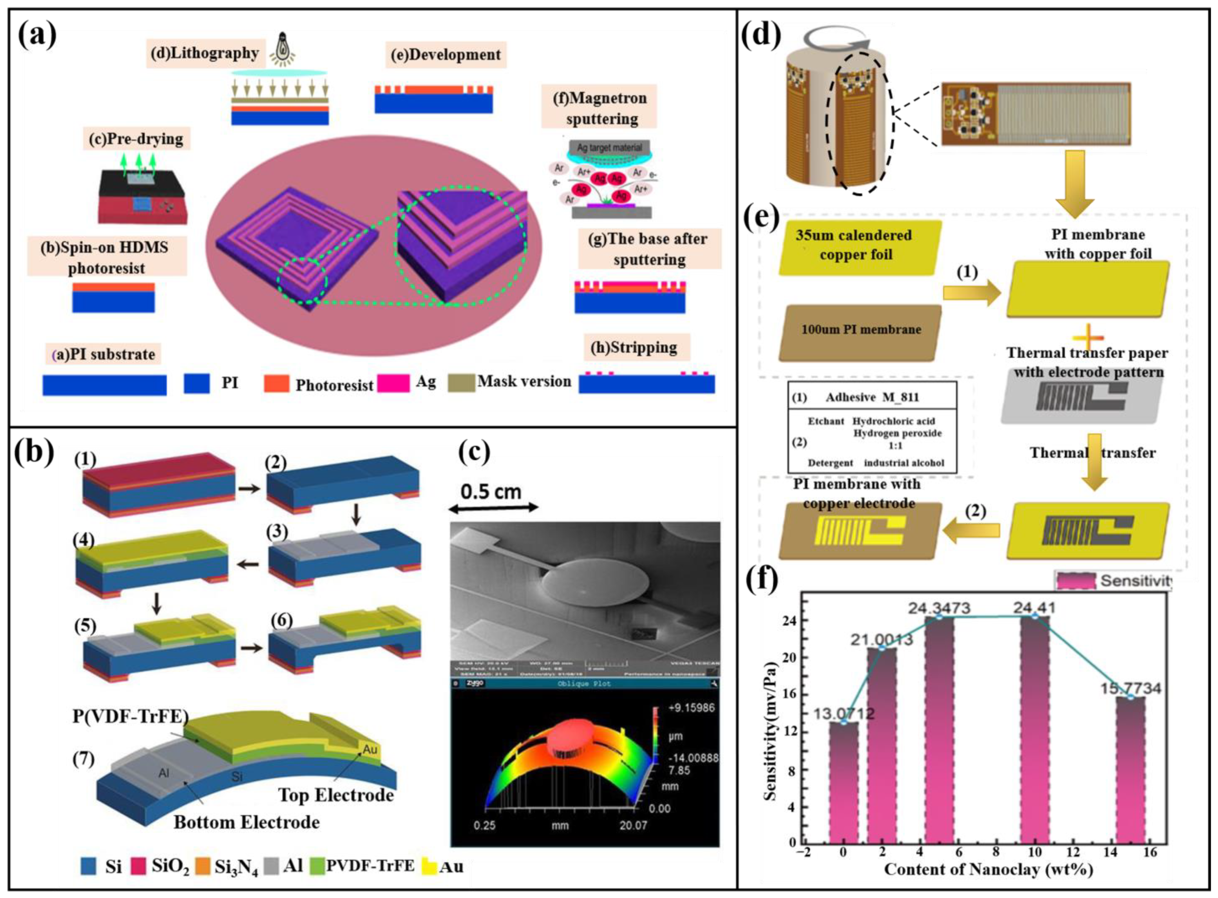
- Xin, Y.; Hou, T.; Liu, C.; Liu, H.; Tong, J.; Li, Y.; Lin, T. Flexible piezoelectric sensor based on PVDF-TrFE/Nanoclay composite nanofibers for physiological micro-vibration signal sensing. Measurement 2022, 201, 111742. [Google Scholar] [CrossRef]


| Types | Mold Area (mm × mm) | Frequency Range (kHz) | Sensitivity | References |
|---|---|---|---|---|
| Resistive type 1 | 5 × 5 | 13.3 | 0.545 mV/g | [51] |
| Resistive type 2 | 3.5 × 3.5 | 1.5 | 4 mV/g | [52] |
| Capacitive type | 6.5 × 5 | 6 | / | [53] |
| PZT | 6 × 6 | 17.4 | 14 mV/g | [54] |
| AlN | 6.8 × 6.8 | 1.1 | 400 mV/g | [55] |
| AlN_C500 | 2.3 × 2.3 | 12.5 | 355 mV/g | [50] |
| AlN_S200 | 2.3 × 2.3 | 42.8 | 176 mV/g | [50] |
| YCOB | / | 0.6 | 2.4 pC/g | [48] |
| BTS | / | 3 | 2.6 pC/g | [47] |
| N/A | / | 6 | 3.5 pC/g | [56] |
| Categories | Materials | Advantages | Disadvantages |
|---|---|---|---|
| FDM | All-plastic materials (PA, PLA, PC, etc.) | Low cost Open-source code | Slow printing speed Low resolution |
| DIW | Ceramics, plastics, hydrogels, and even living cells | Fast printing speed High durability Suitable for repairing components | Subsequent processing required Low mechanical properties Poor surface finish |
| SLA, DLP | Resins, polymers, plastics | High speed High resolution Complex and high-precision structure | Single material Easy to damage the device Support structure required |
| LOM | Papers, plastics, metals | Low Cost High speed Color printing | Post-processing required Low resolution Design limitations |
| SLS, SLM | Plastics, metals, ceramics, waxes | High strength and stiffness Suitable for aerospace and military No support mechanism required | Slow printing speed Size limitation High power usage |
| Ployjet | Photosensitive resins | High resolution, suitable for small and delicate devices | Low strength |
| 3DP | Ceramics, plasters, sugars | Can print simultaneously Color printing No support mechanism required | Poor surface strength and roughness Requires post treatment Low mechanical properties |
Disclaimer/Publisher’s Note: The statements, opinions and data contained in all publications are solely those of the individual author(s) and contributor(s) and not of MDPI and/or the editor(s). MDPI and/or the editor(s) disclaim responsibility for any injury to people or property resulting from any ideas, methods, instructions or products referred to in the content. |
© 2023 by the authors. Licensee MDPI, Basel, Switzerland. This article is an open access article distributed under the terms and conditions of the Creative Commons Attribution (CC BY) license (https://creativecommons.org/licenses/by/4.0/).
Share and Cite
Liao, Y.; Yang, H.; Liao, Q.; Si, W.; Chu, Y.; Chu, X.; Qin, L. A Review of Flexible Acceleration Sensors Based on Piezoelectric Materials: Performance Characterization, Parametric Analysis, Frontier Technologies, and Applications. Coatings 2023, 13, 1252. https://doi.org/10.3390/coatings13071252
Liao Y, Yang H, Liao Q, Si W, Chu Y, Chu X, Qin L. A Review of Flexible Acceleration Sensors Based on Piezoelectric Materials: Performance Characterization, Parametric Analysis, Frontier Technologies, and Applications. Coatings. 2023; 13(7):1252. https://doi.org/10.3390/coatings13071252
Chicago/Turabian StyleLiao, Yaoyao, Hong Yang, Qingwei Liao, Wei Si, Yu Chu, Xiangcheng Chu, and Lei Qin. 2023. "A Review of Flexible Acceleration Sensors Based on Piezoelectric Materials: Performance Characterization, Parametric Analysis, Frontier Technologies, and Applications" Coatings 13, no. 7: 1252. https://doi.org/10.3390/coatings13071252