Abstract
Yellow lasers have attracted much attention due to their applications in biomedicine, astronomy and spectroscopy, and the resonant cavity is an important part of lasers. In this work, the resonant cavity film was studied and prepared using physical vapor deposition (PVD) technology to couple and match the optical properties of Dy,Tb:LuLiF4 crystal to generate yellow laser. In the process of film deposition, the substrate temperature has an important influence on the quality of the film. Therefore, we first investigated the effect of HfO2 film quality at different substrate temperatures. Furthermore, the multilayer film was designed to couple and match the optical properties of Dy,Tb:LuLiF4 crystal. According to the designed film system scheme, HfO2 and UV-SiO2 were used as high- and low-refractive index film materials for resonant cavity film preparation using the PVD technique, and the effect of process parameters on the film quality was investigated. A 450 nm pump laser was used to directly pump Dy3+ to excite and generate the yellow laser. In this process, the excited radiation jump occurs in the crystal, and the generated laser in the new band reaches a certain threshold after oscillation and gain in the resonant cavity, thus successfully outputting a 575 nm yellow laser.
1. Introduction
Yellow laser belongs to the category of visible light sources and has important applications in biomedicine, astronomy, spectroscopy and imaging [1]. An all-solid-state laser is an important method of generating lasers directly or indirectly. At present, the lasers capable of outputting yellow light can be divided into semiconductor lasers, sum frequency lasers, frequency doubling lasers, optical parametric oscillators and Raman lasers [2]. Yellow lasers have been widely researched and applied in recent years.
In 2012, Zhichao Wang et al. used the intracavity frequency doubling characteristics of Nd:YAG laser to output a 561 nm yellow laser with a maximum output power of 60.3 W [3]. In 2016, Jianming Yang et al. applied Nd:YAG and Yb:YAG crystals to generate 1319 nm and 1030 nm fundamental waves, respectively. Meanwhile, they achieved intracavity sum frequency in an LiB3O5(LBO) crystal and outputted a 578 nm yellow laser with a maximum output power of 37.5 mW [4]. In 2020, Chen Y.F. et al. developed a diode-pumped Nd:YVO4/KGW Raman yellow laser, which produced a 579.5 nm yellow laser at 6.8 W at an incident pump power of 30 W [5]. In 2020, Bing Sun et al. reported a 588 nm yellow laser with an output power of 13.7 W using intracavity frequency doubling of Nd:YVO4 Raman laser [6]. In 2021, Heng Tu et al. realized the output of 572.5 nm yellow laser with an average output power of 9.2 W by using a diamond Raman laser and 532 nm green laser as pumping source [7]. In 2021, Lee et al. coated a high-reflection film on a Nd:YVO4 self-Raman laser to improve beam quality and reduce laser threshold, and achieved 6.54 W and 5.12 W output power at 559 and 588 nm [8]. As can be seen, there has been a great deal of research on various types of lasers and ways of generating lasers in the yellow range. In addition, in the process of generating yellow lasers in each of these bands, optical thin films play a crucial role in the generation, conversion and transmission of lasers. The resonant cavity design of a crystal can be used to modulate the spectral characteristics of an optical system and is an indispensable element in a laser system.
Nowadays, researchers have developed a variety of laser crystals in the yellow light range of 570~620 nm in the field of all-solid-state lasers. In particular, Dy,Tb:LuLiF4, as a Raman laser crystal that can emit yellow-orange lasers, has the special advantage of the energy level structure transition of yellow light generated by dysprosium ions to obtain yellow lasers directly, quickly and efficiently [9]. Therefore, plating a specific optical film on the input mirror and output mirror of the resonant cavity is a hot topic for researchers. Based on the optical properties of Dy,Tb:LuLiF4 crystal, the film design of the input and output mirrors of the resonant cavity is crucial for the yellow laser output. In this paper, we have investigated and designed an optical film for coupling and matching Dy,Tb:LuLiF4 crystals to produce 575 nm yellow laser light. For this band of yellow laser, the technical parameters are determined, and the optimal selection of process parameters, theoretical design of the film system and film thickness monitoring scheme of the optical film are explored.
As is known, physical vapor deposition (PVD) is a technology in which thin-film materials are converted from a solid phase to a gas phase and then deposited on the substrate surface. The advantages of evaporation-based PVD techniques are higher purity of the film and better control of the film thickness [10]. According to the requirement of technical parameters, Dy,Tb:LuLiF4 laser crystal is used as the gain medium in this work. Firstly, the resonant cavity films were designed to couple and match the optical properties of Dy,Tb:LuLiF4 crystals. Then, according to the designed film system scheme, HfO2 and UV-SiO2 were used as high- and low-refractive index film materials for resonant cavity film preparation using physical vapor deposition technique and the effect of process parameters on the film quality was investigated. The film thickness monitoring scheme combining quartz crystal control and optical monitoring was used to complete the preparation of the resonant cavity film. The prepared resonant cavity film was put into the optical system, and the 575 nm yellow laser was successfully output by 450 nm laser excitation.
2. Experiments
2.1. Materials and Software
Hf (99.95%, JuBo Guneng Co., Ltd., Suzhou, China Thin Film Materials, UV-SiO2 (99.9997%, JuBo Guneng Co., Ltd., Suzhou, China) Thin Film Materials.
TFCalc(3.5.15, Software Spectra, Inc., Vermillion, SD, USA) software was used to design the film system and analyze the sensitivity of each film layer. MCalc (V4.0.21, Leybold Optics Co., Ltd., Beijing, China) software was used to calculate optical constants of the films and design the optical control monitoring scheme.
2.2. Preparation of HfO2 Monolayer Film
The experiment was carried out in SYRUSpro 1110 vacuum coating machine. Before starting the coating, the substrate material was wiped by used an ethanol ether mixture with a volume ratio of 1:3. In this experiment, high-purity metal Hf particles were used as the initial material, and high-purity oxygen was used as the reaction gas to prepare HfO2 thin films through reaction evaporation. The sputtering phenomenon existing during the deposition of HfO2 thin-film material was suppressed and the nodular defects in the film layers were reduced [11], while stable evaporation of the thin-film material was achieved.
The substrate material for depositing HfO2 monolayer film is BK7 glass with a diameter of 30 mm and a thickness of 1 mm. The substrate temperature of film deposition was set to 120 °C, 150 °C, 180 °C, 210 °C, and 240 °C, respectively, and the other parameters were consistent. The deposition process parameters of HfO2 monolayer film are shown in Table 1. The equipment used for the experiments has one process gas inlet at the electron gun (HPE) and one at the ion source (APS). When oxygen is charged from different inlets, it will react with hafnium in different forms. The oxygen charged from the electron gun is in the form of oxygen molecules, while most of the oxygen charged from the ion source will be ionized into oxygen ions by the collision of argon ions. In order to maintain a constant vacuum, the oxygenation flow rate is set to 50 sccm.

Table 1.
Deposition process parameters of HfO2 thin films at different temperatures.
2.3. Preparation of Resonant Cavity Film
A laser system consists of a pump light, gain medium, and resonant cavity. In this experiment, the pump light was a 450 nm laser, the gain medium was a Dy,Tb:LuLiF4 crystal, the resonant cavity was composed of an input mirror and an output mirror, and the schematic diagram of the laser system is shown in Figure 1. The component near the pump light source is the input mirror of the resonant cavity, and the component away from the pump light source is the output mirror of resonant cavity.
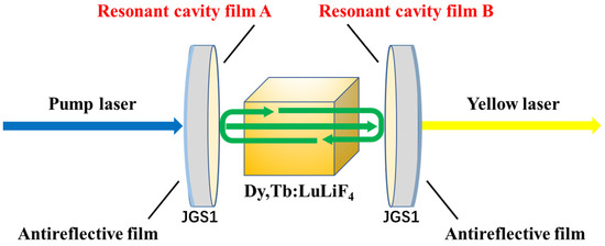
Figure 1.
Schematic diagram of 575 nm all-solid-state laser system structure.
The substrate material of the input mirror and the output mirror is JGS1 fused silica glass with a diameter of 30 mm and a thickness of 2 mm. The surface of the input mirror is coated with resonate cavity film A and antireflective film, and the surface of the output mirror is coated with resonate cavity film B and antireflective film. The technical parameters of resonant cavity film A and resonant cavity film B are shown in Table 2.
Table 2.
Technical parameters of resonant cavity film A and resonant cavity film B.
2.4. Characterization
The structure of the films was measured by an X-ray diffractometer (XRD, SmartLab, Rigaku, Osaka, Japan). The transmittance of the HfO2 films coated at different substrate temperatures was tested using an UV-Vis spectrophotometer (PE1050, Perkin Elmer, Waltham, MA, USA). The surface shape of the substrates with deposited film was characterized by a laser interferometer (G150, Shine Optics, Shanghai, China) with a light source wavelength of 632.8 nm. The cross-sectional morphology of the films was measured by an ultra-high resolution field-emission scanning electron microscope (FE-SEM, Verios 460L, FEI, Hillsborough, OR, USA). The spectrum of the output laser was measured using a high-resolution spectrometer(Aurora 4000, Lyman Optoelectronics Instruments Co., Changchun, China). The power magnitude of the output laser was measured using a laser power meter (Vega, OPHIR, Jerusalem, Israel).
3. Results and Discussion
3.1. Studies of Monolayer HfO2 Film
In the process of optical film preparation, substrate temperature, ion source bias, background vacuum, oxygenation, and deposition rate are the key factors affecting the film quality [12]. Among them, the substrate temperature affects the migration rate of the film material molecules, thereby affecting the degree of bonding between the film and the substrate [13]. Therefore, the effect of substrate temperature on the deposition of HfO2 monolayer film was investigated including the relationship between the crystallization, refractive index, surface roughness, and substrate temperature.
The structure of the film was measured using an X-ray diffractometer of the SmartLab model produced by Rigaku. The XRD results of HfO2 films deposited at different temperatures are shown in Figure 2. When the temperature is lower than 180 °C, no obvious diffraction peak appears, indicating that the film is amorphous. As the temperature further increases, the diffraction peaks intensity of the HfO2 film gradually increase, indicating that the film gradually changes from amorphous to crystalline, and the film exhibits a preferred crystal orientation at the (020) diffraction peak with a diffraction angle of 34.6° and the (−111) diffraction peak with a diffraction angle of 28.3°.
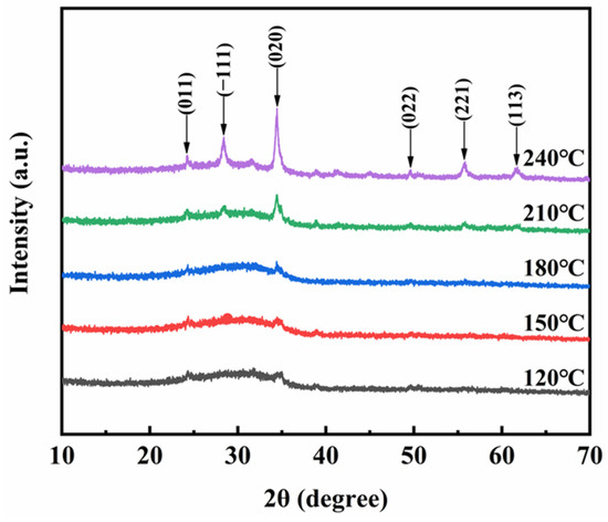
Figure 2.
XRD patterns of HfO2 thin films with different substrate temperatures.
The transmittance of HfO2 films deposited at different substrate temperatures was measured using a UV-visible spectrophotometer, as shown in Figure 3a. According to the transmittance spectrum curve, the refractive index of the HfO2 film was calculated by MCalc software. The refractive index and packing density of HfO2 films under different substrate temperature are shown in Table S2. As shown in Figure 3b, the refractive index of the film at 575 nm increases with the increase of temperature. When the temperature is higher than 210 °C, the refractive index does not change significantly, and the refractive index at 575 nm is about 2.08.
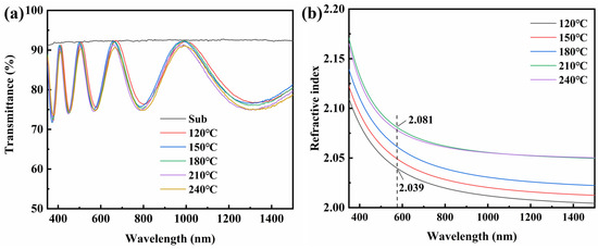
Figure 3.
(a) Transmittance and (b) refractive index curves of HfO2 films at different substrate temperatures.
The surface shape of the substrate was measured by a laser interferometer. The light source wavelength of the interferometer is 632.8 nm. Figure S1 shows the surface shape test diagram of the coated BK7 substrate at different temperatures and the uncoated BK7 substrate. According to the surface shape results, the root mean square (RMS) and peak–valley difference (PV) of the surface roughness of HfO2 films at different temperatures were analyzed, and the results are shown in Figure 4. When the temperature increases from 120 °C to 240 °C, the RMS value has a minimum value of 0.05514λ at 180 °C and a maximum value of 0.14948λ at 240 °C. In general, the RMS values of HfO2 films at different substrate temperatures are small and the surface morphology is uniform.
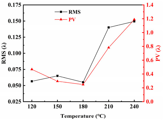
Figure 4.
RMS and PV values of the surface roughness of HfO2 films at the substrate temperatures of 120 °C, 150 °C, 180 °C, 210 °C, and 240 °C.
When the temperature increases from 120 °C to 180 °C, the PV value decreases with increasing temperature and with a minimum value of 0.24813λ at 180 °C. This is due to the increased migration of particles on the substrate surface with increasing temperature, which increases the densities of the film and the bonding ability of the film to the substrate, resulting in a smoother and less defective film surface [14]. In addition, the residual stress between the film and the substrate is low in this temperature range, which also results in lower PV. However, when the temperature increases from 180 °C to 240 °C, the PV increases with temperature, with a maximum value of 1.18894λ at 240 °C. This is because the continued increase in temperature leads to an increase in the bombardment of the substrate by the film molecules, and some film molecules even enter the interior of the substrate because of the rapid migration rate, which causes the surface structure of the film to be inhomogeneous and the defects to increase [15]. In addition, the high temperature also increases the residual stress between the film and the substrate and may lead to problems such as localized peeling of the film on the substrate surface [16].
Considering the results of XRD, spectral and surface shape results, a substrate temperature of 180 °C was used for coating in this paper, and the deposition process parameters of the resonant cavity film are shown in Table 3.
Table 3.
Deposition process parameters of HfO2 and UV-SiO2 materials.
3.2. Theoretical Design of Resonant Cavity Film
Multilayers can be considered as a superposition of monolayers. Therefore, the calculation of the electromagnetic field behavior of multilayers can be understood as the whole set of film matrices being the product of its each monolayers [17].
The multilayer interface of a multilayer membrane can be expressed as an equivalent interface with the optical conductance Y of the membrane surface.
If the film layer system has absorption, the absorption rate can still be deduced from Equation (4). Assuming that neither the incident dielectric nor the substrate has absorption, the light intensity I of the light wave arriving at the k interface is
* indicates conjugate complex numbers.
The actual intensity of the light waves entering the membrane system is
The reflectivity of the film system is set as R, then the actual light intensity entering the film system is equal to (1 − R)I0, where I0 is the intensity of incident light. Next, we compare these two equations to obtain
According to the law of conservation of energy it is then obtained that the absorption rate A is
In addition, from the transmittance a of the monolayer
The reflectance R and transmittance T of the membrane system can also be deduced respectively as
The theoretical film system design of resonant cavity film was carried out using TFCalc film system design software. The resonant cavity film A requires high transmission in the 345~460 nm band and high reflection in the 540~620 nm band. For this index, a short wavelength pass can be used as the base film system, set as Sub|(0.5LH0.5L)^S|Air, where S is the number of repetition cycles of the film stack, Sub is JGS1 fused silica, H is HfO2 with an optical thickness of 1/4 reference wavelength, and L is UV-SiO2 with an optical thickness of 1/4 reference wavelength. The requirement of cutoff in the reflective region is achieved by adjusting the number of repetition cycles S. When S ≥ 25, a high cutoff is obtained in the highly reflection region and a higher transparency is available in the highly transmissive region. After that, with the increase of the repetition number, the cutoff degree of the reflection region and the transparency of the transmittance region do not change significantly. Under the condition of meeting the technical parameters, the number of layers of the short wave pass film system should be as few as possible. The initial film system is set as Sub|(0.5LH0.5H)^25|Air, the reference wavelength is 570 nm.
According to the technical parameters, the optimized continuous target was set in TFCalc software. The final film system was Sub|1.2160H 0.8903L 1.2012H· ·1.2486L 0.7505H 0.6234L|Air, with a total of 50 layers and a physical thickness of about 4.217 μm. Each film layer physical thickness of resonant cavity film A is shown in Table S3. The initial and the theoretical transmittance spectral curve of the resonant cavity film A is shown in Figure 5. It can be seen from the theoretical transmittance spectrum that the average transmittance of 345~460 nm band is 99.5328%, and the average reflectance of 540~620 nm band is 99.9368%, which meets the requirements of technical parameters.
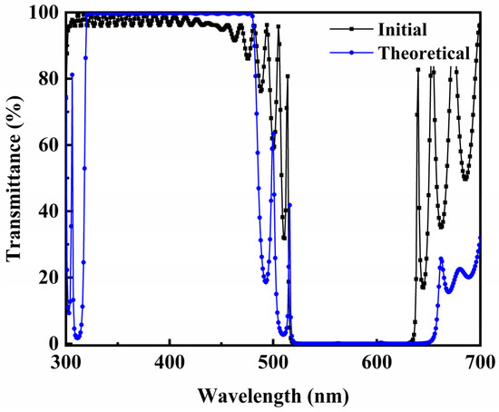
Figure 5.
The initial transmittance curve and theoretical transmittance curve of the resonant cavity film A.
The resonant cavity film B requires high reflection in the 345~460 nm band, transmittance T = 1% in the 540~620 nm band, and multiple high reflection film systems q((HL)^S H) need to be introduced for superposition, where q is the film stack coefficient, and S is the number of repetition cycles of the film stack. The film stack coefficient and the number of cycles of the basic film system are determined according to the reflection bandwidth and reference wavelength of the film system. The initial film system was set as Sub|0.75((HL)^10 H) 0.83L 0.91((HL)^12 H) 1.07L 1.23((HL)^8 H)|Air, with the reference wavelength of 470 nm.
According to the technical parameters, the optimization target was set, and the optimized film system was Sub|0.7142H 0.6986L 0.7482H 0.8190L · · ·1.5647L 1.7563H 1.0586L 1.3936H|Air, with a total of 71 layers and a physical thickness of about 4.826 μm. Each film layer physical thickness of resonant cavity film B is shown in Table S4. The initial and the theoretical transmittance spectral curve of the resonant cavity film B are shown in Figure 6. It can be seen from the theoretical transmittance spectrum that the average reflectance of the 345~460 nm band is 99.9106%, and the average transmittance of the 540~620 nm band is 1.0174%, which meets the requirements of technical parameters.
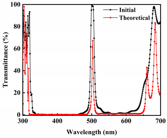
Figure 6.
The initial transmittance curve and theoretical transmittance curve of the resonant cavity film B.
In order to ensure that the pump light is input with high transmittance and the yellow laser is output with partial transmittance, a 330~650 nm antireflective film needs to be coated on the input mirror and the output mirror. The design scheme of the antireflective film was Sub|0.1558H 0.6749L 0.2223H 2.1507L 0.3158H 0.1299L 1.4884H 0.9055L|Air, with a total of 8 layers, a reference wavelength of 240 nm, and a physical thickness of about 0.43 μm. The development process of antireflective film is no longer described in detail due to the relatively simple design of antireflective film and a few numbers of layers. The theoretical and measured transmittance curves of the antireflective film are shown in Figure S2. The theoretical average transmittance of film was 99.5080% in the 330~650 nm band, and the measured average transmittance was 95.76%. Since the exit medium of the film was air during the process of transmittance testing, there was a partial loss of the tested transmittance.
The film systems of the resonant cavity film A, resonant cavity film B, and the antireflective film were imported into the TFCalc software, and the theoretical transmittance curves of the input mirror and the output mirror were obtained as shown in Figure 7. The average transmittance of the input mirror was 99.6246% in the 345~460 nm band and the average reflectance was 99.9369% in the 540~620 nm band. The average reflectance of the output mirror was 99.9378% in the 345~460 nm band and the average transmittance was 1.0378% in the 540~620 nm band.
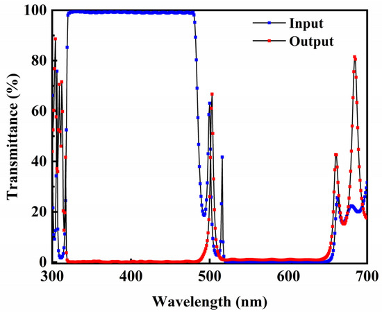
Figure 7.
Theoretical transmittance curves of input mirror and output mirror.
3.3. Analysis of Quartz Crystal and Optical Control Solutions
Current methods of film thickness monitoring include quartz crystal monitoring and optical monitoring [18]. Quartz crystal monitoring can provide the deposition rate of the film layer. However, as the thickness of the film layer increases, the accuracy of the quartz crystal oscillation frequency decreases and the error increases. Especially for highly sensitive film layers, a small error may have a serious impact. Therefore, timely switching of the crystal control chip is required [19]. The optical monitoring method measures the optical thickness of the film and has a compensation mechanism for the film thickness error. However, it is difficult to monitor the deposition rate of the film [20]. Therefore, in order to overcome the drawbacks of each of the quartz crystal control and optical control methods, a film thickness monitoring method that combines the crystal control and optical control methods was used to monitor the film thickness of the resonant cavity film in this work [21].
The first-order film layer sensitivity and second-order film layer sensitivity of the resonant cavity film A are shown in Figure 8a,b. The crystal switching position is set according to the film layer thickness and film layer sensitivity. When preparing resonant cavity film A, six quartz crystal control chips were used to monitor 1~6, 7~15, 16~23, 24~30, 31~38, and 39~50 layers, respectively. The quartz crystal control chip monitoring scheme of the resonant cavity film A is shown in Figure 9a.
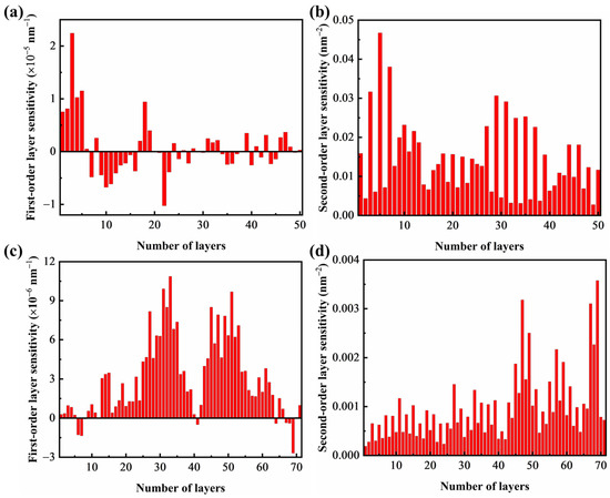
Figure 8.
(a) First-order and (b) second-order layer sensitivity distribution diagram of the resonant cavity film A; (c) First-order and (d) second-order layer sensitivity distribution diagram of the resonant cavity film B.
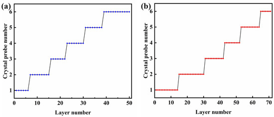
Figure 9.
The quartz crystal control chip monitoring scheme of (a) the resonant cavity film A and (b) the resonant cavity film B.
The first-order film layer sensitivity and second-order film layer sensitivity of the resonant cavity film B are shown in Figure 8c,d. For resonant cavity film B, six quartz crystal control chips were used to monitor 1~14, 15~30, 31~42, 43~52, 53~64, and 65~71 layers, respectively. The quartz crystal control chip monitoring scheme of the resonant cavity film B is shown in Figure 9b.
The design was imported into the MCalc software, and the number of optical control pieces, monitoring wavelength, and other parameters were optimized to determine the optimum monitoring scheme. The number of optical controllers should be as few as possible for the premise of meeting the monitoring requirements to reduce the accumulation of residual errors caused by switching optical controllers during the film deposition process.
Figure 10 shows the variation curves of transmitted light signal intensity with thickness for film layers A and B. It can be observed that the alternating points of HfO2 film (blue curve) and SiO2 film (green curve) are located in the non-extreme values of the optical signal variation curves. At this point, the optical signal is sensitive to changes in the thickness of the film layer, and it is easy to accurately control the thickness of the film layer.
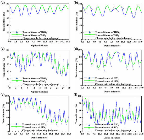
Figure 10.
Optical monitoring design of resonant cavity film A (a) 1#, (b) 2#, and (c) 3#. Optical monitoring design of resonant cavity film B (d) 1#, (e) 2#, and (f) 3#.
Combined with the sensitivity analysis of the resonant cavity film A, when the number of optical control pieces was lower than 3, it was impossible to find a monitoring scheme where the error of each layer can be controlled at 1%. Therefore, the number of optical control pieces in the monitoring scheme was determined to be 3. The 1# optical control chip monitored the 1st to 14th layers, 2# optical control chip monitored the 15th to 26th layers, and 3# optical control chip monitored the 27th to 50th layers. The monitoring wavelengths of the optical control chips were 435 nm, 443 nm, and 486 nm, respectively. The optical signal changing with thickness is shown in Figure 10a–c.
Similarly, combined with the sensitivity analysis of the resonant cavity film B, the number of optical control pieces in the monitoring scheme was determined to be 3. The 1# optical control chip monitored the 1st to 20th layers, 2# optical control chip monitored the 21st to 44th layers, and 3# optical control chip monitored the 45th to 71st layers. The monitoring wavelengths of the optical control chips were 438 nm, 490 nm, and 436 nm, respectively. The optical signal changing with thickness is shown in Figure 10d–f.
3.4. Test and Analysis of Resonate Cavity Film
The cross-sectional morphology of resonant cavity film A and film B was tested by ultra-high-resolution field-emission scanning electron microscopy (SEM). The SEM results are shown in Figure 11. It can be observed that both the resonant cavity film A and resonant cavity film B have densely arranged lamellar structures. The physical thickness of the resonant cavity film A is 4.209 μm, and the relative error with the theoretical physical thickness is 0.24%. The physical thickness of the resonant cavity film B is 4.838 μm, and the relative error with the theoretical design physical thickness is 0.18%.
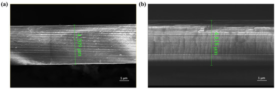
Figure 11.
The FE-SEM cross-sectional micrographs of (a) resonant cavity film A and (b) resonant cavity film B.
The transmittance of the input and the output mirror after the deposition of the antireflective films is shown in Figure 12. The results show that the average transmittance of the input mirror in the 345~460 nm band is 98.61% and the average reflectance in the 540~620 nm band is 99.61%. The average reflectance of the output mirror in the 345~460 nm band is 99.74%, and the average transmittance in the 540~620 nm band is 1.06%. The actual spectrum results meet the theoretical design requirements.
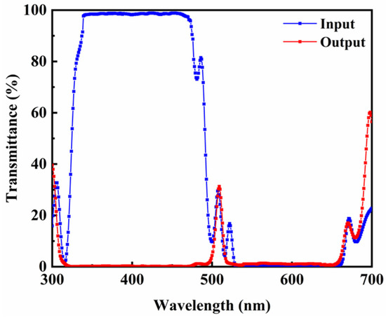
Figure 12.
The actual test transmittance spectral curves of the input mirror and the output mirror.
After the input and output mirrors of the resonant cavity were completed with the film preparation, surface shape tests were performed as shown in Figure 13. The measured PV values for the input mirror and output mirror were 0.36071λ and 0.79648λ, respectively, and the RMS values were 0.08988λ and 0.11702λ, respectively. Compared with the HfO2 single-layer film, the resonant cavity film prepared based on both HfO2 and UV-SiO2 materials has an increased number of layers, and the residual stress between the film layers will be larger. As a result, the microscopic morphology of the multilayer film is more inhomogeneous compared with the monolayer film, and the deformation and surface roughness will be higher than that of the monolayer film. Nevertheless, the PV and RMS values meet the requirements.
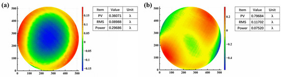
Figure 13.
The surface shape of the resonant cavity (a) input mirror and (b) output mirror.
A Dy,Tb:LuLiF4 crystal with dimensions of 3 × 3 × 25 mm3 was placed in a resonant cavity consisting of an input mirror and an output mirror to complete the construction of the optical path system. In this work, the pump source was a laser with a central wavelength of 450 nm and a fiber diameter of 500 μm. The spectrum and the power of the output laser were measured by a high-resolution spectrometer and a laser power meter, respectively. The laser output results are shown in Figure 14. It can be seen that the plated resonant cavity films were used to couple and match the Dy,Tb:LuLiF4 crystal successfully, causing an excited radiation leap in the crystal, thereby outputting a 575 nm yellow laser with the output power of 106 mW.
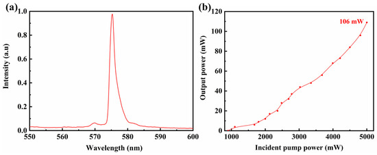
Figure 14.
(a) 575 nm laser output test diagram obtained under 450 nm laser excitation. (b) Laser output power test diagram with 106 mW.
4. Conclusions
A resonant cavity film capable of Dy,Tb:LuLiF4 laser crystal matching and outputting a yellow laser of 575 nm was successfully prepared. The substrate temperature was determined to be 180 °C by plating HfO2 monolayer film on different substrate temperatures and performing XRD, spectroscopy and surface shape measurement, considering the dense film and the residual stress between the film and the substrate. According to the technical parameters, the theoretical film systems of resonant cavity film A surface, resonant cavity film B surface, and the antireflective film were designed, and the crystal control scheme and optical control scheme of resonant cavity film A surface and resonant cavity film B surface were designed. The SEM, spectral, and surface shape results show that the input and output mirrors meet the requirements of the technical parameters and can output a 575 nm yellow laser with the Dy,Tb:LuLiF4 crystal. The film quality has a significant effect on the conversion efficiency of the laser. By optimizing the ion source parameters and the deposition rate of the film, further reducing the film surface roughness and residual stress between the film layers, and enhancing the laser damage threshold of the film to increase the pump light input power will be the key research direction for resonant cavity thin films in the future.
Supplementary Materials
The following supporting information can be downloaded at: https://www.mdpi.com/article/10.3390/coatings13071278/s1, Figure S1: Surface shape test of coated BK7 substrate at different temperatures and uncoated BK7 substrate (a) BK7; (b) 120 °C; (c) 150 °C; (d) 180 °C; (e) 210 °C; (f) 240 °C; Figure S2: (a) Theoretical and (b) measured transmittance curve of antireflective film (when the second surface was not coated, the substrate/air interface reflectance was 3.7% @550 nm); Table S1: Output wavelength and output power of each yellow laser band obtained from previous studies and this work. Table S2: Refractive index and packing density of HfO2 films under different temperature. Table S3: Each film layer physical thickness of resonant cavity film A. Table S4. Each film layer physical thickness of resonant cavity film B.
Author Contributions
Conceptualization, H.Z., Y.X., Y.C. and S.X.; data curation, H.Z., Y.X., Y.C., Y.L., Y.P. and S.M.; formal analysis, H.Z., Y.X., Y.C. and S.X.; funding acquisition, S.X. and Z.H.; investigation, Y.Z. and Y.X.; methodology, S.M., S.X. and Z.H.; project administration, S.X. and Z.H.; resources, H.Z., Y.X. and S.X.; supervision, Y.Z.; validation, H.Z., Y.X., Y.C., Y.P. and S.X.; visualization, Y.X., Y.L. and S.X.; writing—original draft, H.Z. and Y.X.; writing—review and editing, S.X. All authors have read and agreed to the published version of the manuscript.
Funding
Z.H. acknowledges funding by the National Natural Science Foundation of China (project no. 51890865).
Institutional Review Board Statement
Not applicable.
Informed Consent Statement
Not applicable.
Data Availability Statement
The data used in this research are available from the corresponding author upon reasonable request.
Conflicts of Interest
The authors declare no conflict of interest.
Abbreviations
List of symbols
| E | Electric field intensity |
| H | Magnetic field intensity |
| B | Magnetic induction intensity vector |
| C | Magnetic field intensity vector |
| φ | Phase difference |
| δ | Phase of the film |
| λ | Wavelength of electromagnetic wave |
| PVD | Physical vapor deposition |
| UV | Ultraviolet |
| O2 | Oxygen |
| PV | Peak valley |
| RMS | Root mean square |
References
- Tanaka, H.; Kalusniak, S.; Badtke, M.; Demesh, M.; Kuleshov, N.V.; Kannari, F.; Kränkel, C. Visible solid-state lasers based on Pr3+ and Tb3+. Prog. Quantum Electron. 2022, 84, 100411. [Google Scholar]
- Cai, Y.; Ding, J.; Bai, Z.; Qi, Y.; Wang, Y.; Lu, Z. Recent progress in yellow laser: Principles, status and perspectives. Opt. Laser Technol. 2022, 152, 108113. [Google Scholar] [CrossRef]
- Wang, Z.; Peng, Q.; Bo, Y.; Xie, S.; Li, C.; Xu, Y.; Yang, F.; Xu, J.; Zhang, J.; Cui, D.; et al. 60 W yellow laser at 561 nm by intracavity frequency doubling of a diode-pumped Q-switched Nd:YAG laser. Opt. Commun. 2012, 285, 328–330. [Google Scholar] [CrossRef]
- Yang, J.; Tan, H.; Tian, Y.; Yao, W.; Ma, G.; Ju, Q.; Zhang, L.; Chen, J.; Li, Z. Generation of a 578 nm yellow laser by the use of sum-frequency mixing in a branched cavity. IEEE Photonics J. 2016, 8, 1500607. [Google Scholar] [CrossRef]
- Chen, Y.; Chen, C.; Lee, C.; Huang, H.; Liang, H. Efficient solid-state Raman yellow laser at 579.5 nm. Opt. Lett. 2020, 45, 5612–5615. [Google Scholar] [CrossRef] [PubMed]
- Sun, B.; Ding, X.; Jiang, P.; Bai, Y.; Yu, X.; Liu, Y.; Wang, J.; Zhao, L.; Li, T.; Jiang, G.; et al. 13.7 W 588 nm yellow laser generation by frequency doubling of 885 nm side-pumped Nd:YAG-YVO4 intracavity Raman laser. IEEE Photonics J. 2020, 12, 1501607. [Google Scholar] [CrossRef]
- Tu, H.; Ma, S.; Hu, Z.; Jiang, N.; Shen, Y.; Zong, N.; Yi, J.; Yuan, Q.; Wang, X.; Wang, J. Efficient monolithic diamond Raman yellow laser at 572.5 nm. Opt. Mater. 2021, 114, 110912. [Google Scholar] [CrossRef]
- Lee, C.; Huang, C.; Huang, H.; Chen, C.; Tsou, C. Comparison between self-Raman Nd:YVO4 lasers and NdYVO4/KGW Raman lasers at lime and orange wavelengths. Appl. Sci. 2021, 11, 11068. [Google Scholar] [CrossRef]
- Zhang, Y.; Wang, R.; Zhou, Y.; Cao, S.; Lu, D.; Xu, H.; Han, W.; Liu, J. Diode-pumped Dy3+,Tb3+:LuLiF4 continuous-wave and passively Q-switched yellow lasers. Opt. Commun. 2022, 510, 127917. [Google Scholar] [CrossRef]
- Wang, B.; Fu, X.; Song, S.; Chu, H.O.; Gibson, D.; Li, C.; Shi, Y.; Wu, Z. Simulation and optimization of film thickness uniformity in physical vapor deposition. Coatings 2018, 8, 325. [Google Scholar] [CrossRef]
- Yu, Z.; Zhang, W.; Zhu, R.; Qi, H. Structural, optical, chemical and laser damage resistant properties of HfO2 films deposited by reactive electron beam evaporation. Chin. J. Lasers 2020, 47, 0403002. [Google Scholar]
- Li, X.; Shen, J. Research progress in laser induced damage on optical films. High Power Laser Part. Beams 2010, 22, 2237–2243. [Google Scholar]
- Jiao, H.; Cheng, X.; Lu, J.; Bao, G.; Liu, Y.; Ma, B.; He, P.; Wang, Z. Effects of substrate temperatures on the structure and properties of hafnium dioxide films. Appl. Opt. 2011, 50, 309–315. [Google Scholar] [CrossRef]
- Tian, X.; Xiong, S.; Zhang, Y.; Zhang, K. Simulation of thermal stress in ion beam sputtered Ta2O5/SiO2 multilayer coatings on different substrates by finite element analysis. Surf. Coat. Technol. 2019, 362, 225–233. [Google Scholar] [CrossRef]
- Zhang, H.; Le, K.; Wang, C.; Sun, J.; Xu, S.; Liu, W. Influence of deposition temperature on the structure and current-carrying friction performance of Cu films by DC magnetron sputtering technology. Lubricants 2023, 11, 8. [Google Scholar] [CrossRef]
- Chen, W.; Gu, P.; Wang, Y.; Zhang, Y.; Liu, X. Analysis of the thermal stress in infrared films. Acta Phys. Sin. 2008, 57, 4316–4321. [Google Scholar] [CrossRef]
- Haija, A.; Freeman, W.; Umbel, R. Review of the characteristic effective medium approximation: Fundamentals and use in calculating the optical properties of ultrathin layer structures. Phys. B 2011, 406, 4266–4271. [Google Scholar] [CrossRef]
- Dong, S.; Fu, X.; Li, C. Noble infrared optical thickness monitoring system based on the algorithm of phase-locked output current–reflectivity coefficient. Coatings 2022, 12, 782. [Google Scholar] [CrossRef]
- Satoh, T.; Izyan Ruslan, R.; Itoh, K.; Marumo, M.; Akitsu, T. Control and monitoring of the quartz crystal current in the quartz crystal oscillator. IEEJ Trans. Electr. Electron. Eng. 2011, 6, 82–88. [Google Scholar] [CrossRef]
- Shieh, W.; Tucker, R.; Chen, W.; Yi, X.; Pendock, G. Optical performance monitoring in coherent optical OFDM systems. Opt. Express 2007, 15, 350–356. [Google Scholar] [CrossRef]
- Zhang, X.; Qian, Y.; Chang, M.; Jiang, M. Monitoring method for filter film thickness based on the combination of photoelectric extreme value and quartz crystal oscillation. Acta Photonica Sin. 2016, 45, 0631001. [Google Scholar] [CrossRef]


Disclaimer/Publisher’s Note: The statements, opinions and data contained in all publications are solely those of the individual author(s) and contributor(s) and not of MDPI and/or the editor(s). MDPI and/or the editor(s) disclaim responsibility for any injury to people or property resulting from any ideas, methods, instructions or products referred to in the content. |
© 2023 by the authors. Licensee MDPI, Basel, Switzerland. This article is an open access article distributed under the terms and conditions of the Creative Commons Attribution (CC BY) license (https://creativecommons.org/licenses/by/4.0/).