Abstract
The thermionic vacuum discharge method is very effective in that the films obtained using this technology are characterised by a very high degree of adhesion, density and purity because the deposition technique is carried out in high, very high or, if possible, in ultra-very high vacuum conditions with no gas present. When the substrate is placed in vacuum, no heat transfer particles are present, the substrate being heated only by the ion incident on the surface. This advantage recommends the TVD method for deposits on plastics or other thermally sensitive materials. Additionally, this slow heat transfer reduces energy loss, making the deposition method industrially competitive. The paper aims to present theoretical aspects of this type of discharge, compared to typical or more popular plasmas but also to present the achievements of this method and its utility in the thin films production, layers that have specific imposed properties. The practical depositions and applications presented are in the nuclear fusion-related material science and also for obtaining materials for granular structures, used as magneto-resistive coatings.
1. Introduction
A tremendous endeavour in scientific and industrial activities is dedicated nowadays to coatings, surface treatments, as well as to thin film production for a large domain of applications.
The following opportunities are indicative of the high level of interest in surface science phenomena:
The possibility to study the elementary particle interactions at the two-dimensional level of the deposited film.
The ability to drastically change the physical-chemical properties of solid surfaces such as:
- -
- surface colour change;
- -
- improvement of the surface tribological properties;
- -
- surface passivation to environmental corrosion agents;
- -
- surface mechanical hardening;
- -
- surface electronic, luminous changes;
- -
- development of new unique material structures, etc.
As a result, one can save and protect expensive materials, extend the life of various device components, save energy, obtain new sources of energy, particularly through solar energy conversion, obtain the most sophisticated layers for automation and IT components, and push up new ways to obtain energy from thermonuclear devices, among other things.
Many deposition and surface treatment technologies are in use nowadays due to their importance in both economic and research activity.
Among these, the following ones are worth being mentioned:
- a.
- Sputtering of cathode material by ion bombardment during the electrical discharges in noble gases, mostly argon;
- b.
- Chemical and plasma assisted chemical vapor deposition method where the electrical discharges in chemical gases can produce active chemical reaction on the surfaces and as a result, can cover them with different thin coatings, such as evaporations by material heating and subsequent deposition, evaporation by laser surface bombardment followed by material deposition, plasma jet deposition, anodic vacuum arc (AVA) deposition and thermionic vacuum arc deposition (TVA).
Of course, there are additional deposition techniques, but we will only be focusing on the last coating method within the scope of this review article because it has highly fascinating qualities that are less well recognized in the scientific community. There are some observations that must be made from the very beginning of this presentation concerning even the denomination and these are the following: after this deposition process was discovered in the eighth decade of the past century, it was given the current name, the thermionic vacuum arc deposition method. However, this method can be used with discharges ranging from modest currents of roughly a hundred mA to proper arc discharges with currents of tens or even hundreds of amperes.
As will be demonstrated on the following pages of this work, it is possible to maintain the vacuum discharge at low currents due to cathode heating by a special external source that ensures sufficient thermo-electron emission from the cathode, capable of igniting and maintaining the small current vacuum discharge, even in high vacuum conditions. Therefore, a more proper denomination of this method would be the thermionic vacuum discharge (TVD) method which includes both small current-high voltage discharges and the high current, small voltage ones. These two modes of discharges, as it will be revealed further, are able to be used when increasing the injected power into the plasma.
When treating the subject throughout this review article, the term “TVD” will be used instead of “TVA” which, as will be seen, represents only a particular domain of the more general one, namely TVD.
2. General Description of the TVD Method
The TVD method consists of a discharge that runs in an atmosphere of pure vapours generated by the anode which in turn, is heated by the energetic action of the electrons coming both from the heated cathode and from the plasma.
The thermo-electrons first emitted by the cathode are accelerated in high vacuum conditions towards the anode on which a high positive potential is applied. This way, the anode material, heated by energetic electron bombardment, is evaporated, and a pure vapor atmosphere is created around the anode whose pressure increases and the necessary conditions appear for plasma ignition by electron-vapor particle collisions. These space particles, neutral or ionized, are expanding in the surrounding vacuum, and are deposited on the probe substrates. Due to the thermo-electrons emitted by the externally heated cathode, the plasma can be started, maintained and changed beginning with very low discharge currents and high anode voltages (tens of milliamps-and kilovolts, respectively) and continued up to hundreds of A and some volts.
In order to have a more detailed introspective view into the physical phenomena, firstly, some general considerations over the cathode, anode and plasma events must be considered further.
2.1. Cathode Phenomena
Imagine a tungsten filament intensely heated by a low voltage, high current electrical source. The energy electron distribution function (Fermi distribution) within a solid at the equilibrium can be simply obtained as follows [1,2]:
Let w1 and w2 be two discrete energy levels inside the solid which are occupied by two electrons which are colliding with each other. After the collision, they are transferred on the new energy levels, w′1 and w′2.
Let p(w) be the probability for an energy level, w, to be occupied by an electron. Then, due to quantum effect, the probability for that energy level to be free is given by 1 − p(w) so that the probability for that energy level to be occupied or non-occupied is p(w) + 1 − p(w) = 1 = certitude.
The probability to have a collision between two electrons having energies w1 and w2, is proportional with the product p(w1). p(w2)[1 − p(w1′)][1 − p(w2′)] states that the levels w1 and w2 must be occupied and the levels w1′ and w2′ must be free for such a collision to appear. Similarly, the inverse collision can be produced proportionally with the probability p(w1′) p(w2′)[1 − p(w1)][1 − p(w2)]. At the equilibrium, the two expressions are equal, and dividing both members of the obtained equation by the product p(w1) p(w2)p(w1′)p(w2′), one obtains:
where the energy conservation w1 + w2 = w1′ + w2′ was considered, Δw being given by |w1 − w1′| = |w2′ − w2| = Δw.
A solution of this equation, as directly seen, is [1/p(w) − 1] = a1exp(a2w). Finally, the probability for the energy level w to be occupied is given by [2].
Now, the constant a1 can be written in a different, more convenient way as a1 = exp(−wF/kT), and a2 as 1/kT. The Fermi-–Dirac distribution that prescribes the number of electrons having the energy w, within a unit space of the solid, is given by:
Here, n is the total number of electrons found within a unit space of solid and this formula shows that the number of electrons with energy w is given by the product of total number of electrons existent in the unit space volume multiplied by the probability to find an electron with that energy [p(w)]. It must be underlined that the constant a2 was chosen to obtain the usual Maxwell–Boltzmann distribution function for the high energy values (w >> wF) when the discrete energy spectrum tends to be continuous and when
Now, the expression of the emission current from the unit surface of the emitter is obtained from Jx = ∫ef(w)g(w)vx(w)dw. Here, x denotes the perpendicular axis on the emitter surface, and g(w) is the density (per unit energy interval) of the possible energetic states for the electrons inside the solid [3].
To evaluate this energy state density, the simplest energetic scheme within the metal, which is that of free electrons, will be considered further.
The corresponding single-dimensional (x) Schrodinger equation is with Ψ as the wave function, as the Plank constant, m as the electron mass and w as the total electron energy. Its solution is a sum of sine and cosine functions and must be zero at the solid boundaries. From these conditions, the arbitrary coefficient of the cosine part of the solution disappears while from the sine part, one obtains that the wave number, kx, must be given by kx = nx π/L with nx—an integer, and L—the maximum length of the solid along the x direction. This relation says that kx can have only discrete values separated from one another by the π/L value. Then the total number of levels existent for a given k2 = kx2 + ky2 + kz2 is obtained as N = 2.4/3πk3(1/8) (π/L)−3 where the volume of only one eighth part of the k space, together with the levels splitting due to the electron spin orientation, were considered [3]. This volume was divided by the k space volume corresponding to an energy state, namely (π/L)3 to obtain the total number of states for a fixed k2 value.
The density of states on the unit energy interval is readily obtained by deriving this expression with respect to the energy (that is dN/dw = (dN/dk)(dk/dw)). Considering that w(k) = 2k2/2m, finally the energy state density is given by g(w) = .
Therefore, the expression of the Jx current can be obtained from:
Here, the transition from the energy-space to velocity-space was made and the condition (w − wF) >> kT was considered. The vx,min is the minimum x component of electron speed value, necessary to overcome the solid energy barrier, (Φ = work function) and to escape into the free space. Performing the well-known integrals appearing here, one obtains the expression for the electron emitted current from the unit solid surface as [4]:
where e is the elementary charge, m is the electron mass, k is the Boltzmann constant, h is the Planck constant, T is the filament temperature and Φ is the barrier encountered by the electron on his way out of metal, which is the minimum energy. A particle of unit electric charge must have to be able to exit the solid and become a free particle. This energy is usually denoted by a work function and is a characteristic value for an electron emitting solid [5].
One can see the exponential increase of the emitted current with the filament temperature. To generate a considerable thermo-emission current, the filament must be heated to a significant temperature, but this temperature must not exceed the melting point of the electron emitting material under the obvious conditions.
The well-known materials that meet these requirements are tungsten, rhenium and carbon, with the first being the most utilized. There are also other metals with high enough melting points, but their high commercial prices forbid their industrial use for thermo-emission purposes.
Here, it must be underlined that different particles of other material adsorbed on the emitter surface contribute to emitter work function; (Φ) changes and it exponentially influences the thermo-emitted current value, as seen from the relation (3).
Usually, a high intensity thermo-electron emission is desired.
A possible way to improve this parameter is to use a thorium-tungsten alloy; when heated, the thorium metal migrates towards the tungsten filament surface and contributes to a work function decrease (Φw = 4.5 eV, Φth = 3.71 eV) and consequently, to a thermo-electron increase.
Assuming an “atmosphere” of vapours generated of other material is present near the emitter surface, these vapours could appear when the anode material is evaporated by electronic bombardment. To appreciate the phenomena taking place in this case, the following considerations will be made.
The evaporated atoms are adsorbed on the solid emitter surface, where they remain for a period before being incorporated by the adsorbing material or leaving the surface by thermal desorption. The atom (molecule) desorption rate from the solid surface can be described by the Equation (5):
where Nads is the total number of the adsorbed particles on a unit surface of the solid, f is a special term closely related to the vibration frequency of the adsorbed particles [5], H is the desorption energy barrier that an adsorbed particle must surpass when leaving the solid surface and Tfil is the filament (solid surface) temperature.
At equilibrium, this particle flux directed away from the surface must be balanced by the oncoming chaotic particle flux from the adjacent space on a unit solid surface.
If the space particle density is Ng, in the condition of chaotic particle movement, half of them have a speed component oriented towards the solid surface, the other half having the speed oriented away from the solid. The space mean value of this unidirectional speed component is also a half of the thermal mean particle velocity because it is comprised between zero and the maximal value of the cosine function. Therefore, the oncoming flux is .
However, the mean thermal speed value, , can be obtained when using the Maxwell distribution function [6,7,8] and is given by the expression vg = , Tg being the space vapour temperature.
At last, the following equation for the oncoming flux towards the unit surface of the emitting metal is derived (which is equal with the flux leaving the unit metal surface at thermal equilibrium (4)): .
where M is the mass of the adsorbed particle and k is the Planck constant. At thermal equilibrium, this incoming particle flux is equal with the number of desorbed particles per unit time and one can write for the adsorbed particle number on the unit surface of the solid surface:
Now, if Nw is the total adsorbing sites existing on the solid surface unity, the occupancy degree of sites on the solid unit surface is given by:
Normally, the energy barrier, H, depends on this coverage degree too, but at higher temperatures of the emitter, it can be assumed that the coverage ratio is low enough and does not influence the barrier value.
The weighted solid work function, φm, influenced by this coverage degree may be written as [9]:
φm = (1 − θ)φw + θφads = φw + θ(φads − φw)
Here, φw is the work function of the solid clean surface (filament = tungsten in the present case), φads—the work function of the adsorbed material.
This relation shows that the greater H, Tg and Ng values are, and the lower Tfil is, the greater the change of the work function for a filament material—adsorbed metal combination.
If φads > φw, then the adsorbed material increases the work function of the solid (filament) and adsorbed material combination (and consequently decreases the thermo-emission) while, when φads < φw, the combination work function decreases (as in the case of a tungsten-thorium combination) and the thermo-emission current increases.
These considerations are useful to be aware of in TVD deposition processes [7].
2.2. Anode Phenomena
When a high positive potential is applied to the emitter potential (which is assumed to be zero), the electrons produced by the heated cathode move through the vacuum space towards the anode and bombard it with high energy. The anode material is thus evaporated. Now, certain considerations will be made in order to better understand the phenomena that have emerged in this case. Suppose a thermal equilibrium existent between the two phases of the evaporating anode material, one being the solid phase and the other one the vapor phase.
Considering the free enthalpy for the unit mass as given elsewhere [10]:
where μ is the free enthalpy, u is the internal energy, p is pressure, v is volume, T is temperature in K and s is entropy. From the free enthalpy expression, it immediately results:
Μ = u + pv − Ts
dμ = du + pdv + vdp − Tds − sdT = vdp − sdT
Here, the principle of thermodynamics, dq = Tds = du + pdv, was considered.
If the two phases are in equilibrium, the free enthalpy variation when passing from one phase to the other one is zero.
This means, when identifying the solid phase with index “2” and the gaseous phase with index “1”, that one can write:
v1dp − s1dT = v2dp − s2dT and therefore (v1 − v2)dp = (s1 − s2)dT
However, from the second law of thermodynamics [11], s1 − s2 = ∫dqrev/T, where qrev is the reversibly transferred heat, when passing from a phase to another one.
In this particular case, the phase change is made by vaporization or condensation and the heat change can be calculated by considering the heat of transformation, usually denoted by λ which can be assumed constant in a first approximation (which really, is not quite exact [12]). Then passing from a solid state to a gaseous one, s1 − s2 = ∫dqrev/T = λ/T and if λ is considered constant, one can write:
which is just the Clausius–Clapeyron Equation (10).
dp/dT = λ/(v1 − v2)T
However, the solid volume (v2) subjected to transition is by far less than the corresponding gaseous one (v1) which in turn is subjected to the universal low of gases, namely pv1 = γNavkT, with γ denoting the number of molls per mass unity, and Nav denoting Avogadro’s number [12].
In conclusion, the following relations could be derived:
which leads to the expression for the gaseous phase pressure value lnp = lnC − λ/γNavkT, or
dp/dT = λp/(γNavkT2)
p = C. exp(−w/kT).
Here, w = λ/γNav is the heat involved when a particle passes from a phase to another and C a constant appearing after integration.
This is the principal dependence form of vapor pressure against the temperature. The true experimental dependence is given in the literature [10], and it is expressed as follows:
where A and B are two constants, characteristic to each substance as suggested by Equation (10). Additionally, a lot of graphs are given elsewhere [13], representing the temperature dependence of the vapor pressure.
p = A exp (−B/T)
As known from statistical mechanics, p = nkT [6], with n being the particle space density. One can conclude that nkT = C.exp(−w/kT).
Whence the vapor gas is formed, a particle flux appears, expanding from the anode to the vacuum space. In this case, that flux continues to travel until it reaches a solid surface where the particles are deposited and do not return to the anode.
Therefore, in stationary conditions, this flux must be sustained by the evaporation rate. However, as presented above (Equation (5)), this flux for equilibrium condition can be expressed as:
or after some arithmetic,
φ = 1/4 n [8kT/(πm)]1/2 = p/(4 kT).[8kT/(πm)]1/2
φ = p(2πmkT)1/2
This is in fact the evaporation rate of the solid phase to vapor phase measured in the number of particles leaving a solid unit surface during a unit time.
For practical reasons, the above given relation must be transformed to a relation which contains the mass quantity evaporated within a second from a square centimetre of anode surface. This is necessary to evaluate the deposition rate which is usually measured by the quartz balance gauges.
In addition, because the vapor pressure dependency on temperature is frequently provided in the literature as measured in torr, a correction factor must be inserted in Equation (11) to allow for this pressure unit translation. Suppose one wants to obtain a formula which gives the evaporation rate in . Equation (11) gives the number of particles evaporated from a square centimetre of evaporating material during a second and in order to transform it in , one must multiply ϕ by M/NA because ϕNA gives the evaporation rate in the number of moles and Mϕ/NA gives the evaporation rate given in since M represents the molar mass which is given in grams.
Multiplying the right side of Equation (11) with this factor, one obtains:
V (in g × cm−2 s−1) = (2πκNA)−1/2 p (in dyn/cm−2) (M/T)1/2
Taking the value of the Boltzmann constant as 1.381 × 10⁻¹⁶ erg/K and the value of NA = 6.022 × 10²³, the (2πκNA)1/2 = 22.8 × 10³ erg/K.
Now, if p is taken from the literature with its value in torr, it is necessary to multiply this value with the correction factor to express p in dyn/cm2, as determined by the measuring units considered in Equation (11).
This can be carried out by taking the mercury density as 13.53 g/cm3, the earth gravity as 981 cm/s2 and the height of a mercury column of 0.1 cm; the pressure correction factor is readily obtained as 1327.3 [dyn/cm2] per torr.
Introducing all these data in the above equation, one obtains for the evaporation rate from a unit anode surface heated to a temperature T(K):
In conclusion knowing the anode temperature, T, and the evaporated particle molar mass, M, the vapor pressure together with evaporation rate can be obtained computationally or from the graphs plotted for a certain material [14]. Conversely, measuring the evaporation rate, the anode temperature together with vapor pressure can be derived.
These values can then be used in the TVD deposition technology.
Indeed, knowing the evaporation rate and the vapor pressure, it is possible to derive the deposition rate on a substrate mounted on a holder which is positioned just above the anode evaporating material (specifically the anode).
The evaporate quantity indicated by Equation (12) expands isotopically in the surrounding vacuum space, generating spheres of increasing radius through which the vapor particles pass every second. This is due to flux conservation, as there are no additional sources or sinks between the punctual anodic source and the chamber’s wall. As a result, the evaporated substance leaving the anode at the rate provided by Equation (12) passes later via a sphere on which the substrate and source are positioned, as shown in Figure 1a.
As a comparison, all of this happens as when blowing the air through a tube with soap and a sphere is formed at the tube tip, or as when inflating a spherical balloon.
The image of this sphere is given in the Figure 1, and it can also be seen in the discharge photo given in the Figure 2, which is obtained when igniting TVD in copper vapours. (This sphere seems to be a little bit elongated along the vertical direction due to the influence of electric fields upon the charged particles but not upon the neutral ones).
In this case, one can write (considering the particle conservation in space):
S.v = 5.83 × 10⁻²S. p(M/T)1/2 g/s = 4πr02q
Here, S is the anode-emitting surface and q is the weight of the evaporated material which crosses during unit time, the unit surface of the sphere on which the substrate is mounted having its normal pointing to the centre of the respective sphere (of uniform coating, as found by Knudsen [15]).
From Equation (13), the deposition rate can readily be found for the mentioned position of the substrate, namely:
d = q/ρ = 1.85 × 10⁻² S(M/T)1/2p/(4r02 ρ) = 1.85 × 10⁻²S(M/T)1/2p/(r2ρ) (m/s)
Here, the deposition rate is given, d (in m/s), at a distance r = 2r0 from the anode (taken along the vertical just above the anode in cm), function of the anode temperature, T (K), molar weight of the anode material, M (g/mol), vapor pressure, p (torr), and density of the depositing material, ρ (g/cm3). This deposition rate is the same all over a sphere which passes through the source (anode) and substrate as proved experimentally by Knudsen and has the radius r0 [16], as shown in the Figure 1. The Knudsen formula also contains the base pressure (which is the minimum gas pressure allowed by the vacuum pump system) which is subtracted from vapor pressure, but in this case, this pressure is negligible in comparison with the pressures of the vapours of the anode material used in deposition. In fact, the Knudsen formula is:
Here, besides the above presented magnitudes and those shown on Figure 1b, the base vacuum pressure pb appears too. From Figure 1a, one can see that r = 2r0 cosθ cosφ (θ = φ) so that for a substrate mounted perpendicularly on the sphere radius r0, no matter its position on that sphere, Rm/ρ is given, as in Equation (14), with r being the distance from the anode to any substrate position on the sphere. When the substrate is positioned nearer to the source, what gains by the distance shortening loses due to the tilting angle.

Figure 1.
Geometry of the deposition from a schematic anode considered similar with Knudsen cell. (a) the spherical surface expansion; (b) with a substrate placed within the sphere. Reprinted/adapted with permission from Ref. [16]. © 2007, Wiley Online Library.

Figure 2.
Plasma image (a) and spatial distribution of plasma potentials for different discharge voltages (b) [12].
In Figure 1 the deposition geometry together with the uniform deposition sphere determined by the anode position and by the substrate position are shown.
For the case of other substrate orientations, the cosine rule must be considered as shown in the given Knudsen Formula (15).
2.3. The Inter Electrode Phenomena
Now, if the anode material temperature is sufficiently high, the vapor pressure increases to a value able to allow for plasma formation (above the anode) by electron-vapor particle ionizing collisions.
The potential of just formed plasma, which is a conductive medium in intimate contact with the anode, will follow the anode potential increase or decrease. However, the plasma potential will always be smaller than the anode potential (at least for discharge currents used in TVD technology), as it will be shown later in this review article.
That means that near the anode, a positive potential jump will appear, which ensures the plasma electron acceleration to produce the continuous evaporation of the anode and to maintain the stationary function of the discharge.
In Figure 2a, TVD plasma is shown together with the line along which the plasma potentials were measured using an electron emission probe. In the right figure, the measured plasma potentials are given for different anode potentials, namely 850 V (red), 750 V (green), 700 V(pink) and 600 V (black). The space origin was chosen as the anode position.
From the potential distribution curves experimentally measured, it is clearly seen that a positive potential jump is formed near the anode in order to accelerate the plasma electrons towards the anode, as mentioned above.
When increasing the anode potential, the plasma density and conductivity will also increase. This increases the plasma current and number of electrons flowing towards the anode. In turn, it will decrease the anode potential fall necessary to maintain the evaporation rate because in this case, the number of electrons is increased.
Furthermore, the plasma potential is seen to be of the order of hundreds of volts and is practically constant along a vast discharge space in the inter electrode gap.
As will be presented further, a lot of interesting peculiarities of this kind of discharge appear.
By this technology, one can see that a continuous deposition of the chosen anode material is processed in high vacuum conditions, being assisted by a high energy ionic bombardment of the just-forming layer.
It is worth noting that the nature of the ions is identical to that of the evaporated particles, and that no gas is present in the deposition chamber. Furthermore, as previously stated, the energy of these ions can be easily adjusted by adjusting the anode potential. More details will be given later.
3. Different Arrangements of TVD Components
3.1. Electron Gun Arrangement for TVD
Figure 3 shows the standard experimental setup, where an electron gun is used as a cathode which is mounted and tilted at an angle with respect to the vertical traced up from the anode.
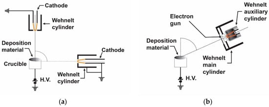
Figure 3.
Electron gun TVD arrangement with different cathode positions: (a) the cathode angle is 90° and (b) the cathode tilt angle is greater than 0°.
The discharge parameters together with the deposition efficiency drastically depend on this cathode tilt angle relative to the vertical line. The plasma burning conditions are better at low tilt angles, but the open space available for deposition is limited. On the contrary, high tilt angles result in harsher burning conditions (higher discharge voltages), but more open space for deposition.
The substrates to be covered with deposited material are placed above the anode when the cathode tilt angle, ά, is greater than 0° Figure 3b.
The possibility to tilt the cathode position allows the heated anode to be exposed to the electron bombardment of the filament but also to have a geometry that allows the plasma and the particles to expand towards the sample holder.
One can see a Whenelt cylinder around the filament dedicated to providing an easier discharge breakdown in anode vapours due to its electron lens action on the anode surface.
Indeed, the role of this cylinder is to facilitate a good electron concentration on the anode surface before the discharge ignition. This way, the electron heating is concentrated on a small anode area and the evaporation becomes more effective, as in the case when the Whenelt cylinder is not present and the electron beam spreads over the greater area.
To understand the electron concentrating action of a hole as that of the Whenelt cylinder, in Figure 4, an oversimplified action is schematically presented (on the electrons) of a potential electric field combination determined by a metal hole, situated between two electrodes, all being mounted in vacuum space.
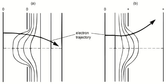
Figure 4.
Schematic potential (a) and electric field distribution (b) around an aperture.
The constant potential lines are marked together with the electron paths, as determined by the electric forces, when different potentials are applied on the cathode, aperture and anode. A deeper look inside the study of the electron optics phenomena can be found in [9,17,18].
As seen from the above presented scheme of the electron gun arrangement, the Whenelt cylinder can be considered as being the focusing hole given in Figure 4, with the filament as the grounded cathode, and anode as the positive electrode shown on the right side of the same figure.
From Figure 4, one can see that, depending on the potential applied on the Whenelt, when the filament is earthen and the anode is at a high positive voltage, the electrons can be concentrated on the surface of the anode, or diverged, just before the discharge is started. The concentration action acts only when it is necessary to concentrate the electrons on the anode to decrease the breaking down potential. Following that point, plasma substantially perturbs this potential distribution and its concentrating impact; however, this effect is no longer required because the discharge burns at lower voltages.
From these considerations, when the Whenelt cylinder is mounted insulated from the filament and a particular voltage is applied on it, the thermo-emitted electron beam can be concentrated at different distances from the filament where the anode is fixed.
In this case, the ignition moment can be optimized for lower anode voltages, and this can lessen the construction conditions imposed to the discharge source. This way, its maximum voltage can be lowered.
In addition, the ignition voltages can be reduced by increasing the cathode heating current, as discussed further in this review article.
Further considerations concerning the electron movement in the electrical fields in vacuum can be found in [9].
3.2. Ring Cathode TVD Arrangement
Another TVD arrangement is presented in Figure 5 which is known as ring cathode TVD. This arrangement was first described in [11].
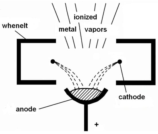
Figure 5.
Old ring cathode TVD (TVA) arrangement. Reprinted/adapted with permission from Ref. [11]. © 1996, European Physical Society.
Here the previously described electron gun arrangement was replaced by a tungsten ring mounted just above the anode material.
The Whenelt cylinder was replaced by a complicated piece, described in Figure 5.
The subsequent versions of ring cathodes, as shown in Figure 6, utilized a simpler Whenelt cylinder, allowing for a much more practical opening space in front of the probe substrates.
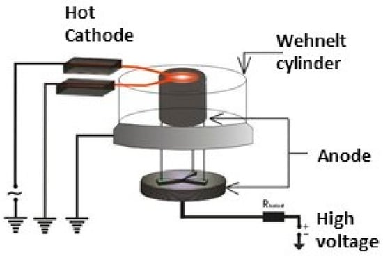
Figure 6.
The new ring cathode structure.
This allowed for a higher deposition rate with this geometry.
The evaporated atoms and generated ions pass through the cathode ring and are deposited on the above mounted substrates.
The deposition rates are greater this time, compared with those obtained by the electron gun arrangement.
Here, the plasma flows through the cathode ring towards the substrates which is different from plasma jets generated in a usual plasmatron type installation, where the plasma flows through the hole drilled through the anode.
Two main technological differences appear directly when using these two structures:
- In the case of the electron gun structure, the highly positive anode is openly “seen” by the earthen probe substrate. As plasma potential is situated near the anode potential, as mentioned above, the plasma ions coming to the probes are accelerated towards and bombard them with energy of the order of eVp which frequently, can be situated around one keV. This will contribute to building up a good, structured coating on the substrates.
However, because plasma ions are mostly directed to the cathode, when the ionization rate increases in comparison to the particle evaporation rate, some unusual behavior of the deposition rate appears, as seen below.
Indeed, the deposition rate can decrease when increasing the power introduced into the plasma.
- 2.
- In the case of ring cathode structure, the probe substrates are directly “seen” by the anode and the ions are guided this time towards the probes contributing aside with atoms to a continuous increase in the deposition rate as the introduced power in the plasma is increased.
On the other hand, because the earthen cathode ring is now positioned between the anode and probe substrate (at zero voltage), a partial electrical screening between anode and substrate develops. This in turn will decrease the energy of ions coming to the forming deposition.
To summarize, the gun cathode configuration ensures a higher ion energy bombardment of probes whereas the ring cathode geometry gives a higher deposition rate with lower ion energy.
However, in the case of conducting substrates, the ion energy can be increased by applying a negative bias on them.
4. TVD Considerations from the Electrical Point of View
In order to evaluate the temporal evolution of the discharge electrical parameters during the TVD ignition for a silver plasma, keeping the cathode-anode distance constant at 5 mm and the filament current at 48 A, we acquired the inter-electronic current and voltage as it is plotted, along with the discharge power in Figure 7, previously published in [12].
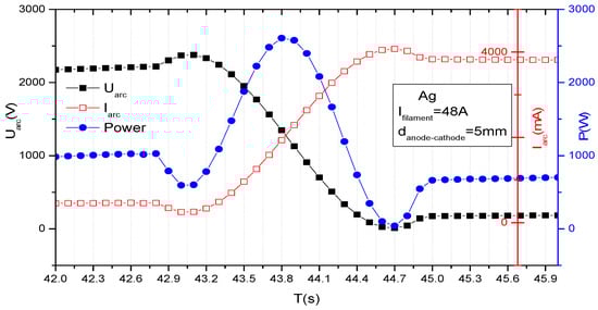
Figure 7.
Example of temporal evolution of current, voltage and power during TVD ignition.
Starting with cathode filament heating that ensures a thermos-electron current of the order of 0.1 A. in high vacuum conditions, when applying high positive voltage on the anode of the order of kilovolts, the current, voltage and power vary as time passes. Here, one can see that the maximum power is obtained (at t = 43.8 s) after the plasma ignition moment (t = 43 s) and becomes smaller after the stationary plasma conditions are attained (t > 450 s).
A possible explanation of time variations of the voltage applied between the anode and cathode, and of the discharge current, may be given as follows:
For the time, t, running in the domain interval, 42 s < t < 42.75 s. the applied voltage, Udisc, together with electron current, Idisc, coming from the heated cathode (there is no plasma yet) are practically constant. That means that the applied voltage can sweep all the electrons thermo-emitted by the cathode. The electron bombardment of the anode creates an atmosphere of vapours around the anode which can create a slowdown of electrons by the newly appeared electron-atom collisions, and temporarily decrease the electron current (no ions are yet produced). The discharge current decrease causes a voltage decrease on the load resistance mounted in series with the discharge and a voltage applied on the discharge increases, as shown on the figure. In this circumstance, the vapor ionization can blow-up, resulting in an increase in the discharge current. Therefore, the voltage applied on the load resistance increases and the remaining voltage available from the source, which is applied in series with burning plasma, decreases. During these transient phenomena, the applied power attains maximum value at approximately 43.8 s, when the space atom density is increasing. The discharge current continues to increase and consequently the applied voltage continues to decrease, attaining its maximum (minimum) value at t = 44.7 s. when the power on plasma becomes minimum. Here, the evaporation rate is expected to decrease, and the ionization rate is expected to decrease too. Consequently, the discharge current decreases and the discharge voltage increases, leading to a slight increase in discharge power until t = 45 s when the stationary state of the discharge is obtained. For t > 45 s, the plasma voltage, current and power are stationary, as seen on the curve.
The used electrical circuitry is presented in the Figure 8. The discharge chamber, as well as the electron gun and anode setup, are sketched. The electrical circuitry for ring cathode filament is similar but the filament, anode and Whenelt positions are changed in a way which will be shown later.
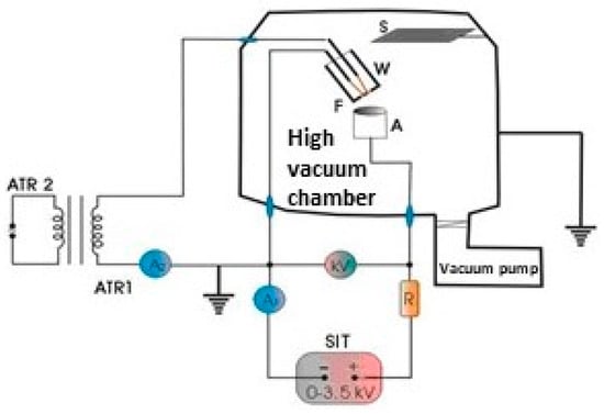
Figure 8.
The electrical circuitry.
The voltage is measured between the anode and the cathode while the current corresponds to that flowing through the discharge, load resistance, R and the high voltage source.
The temporal discharge evolution V-I characteristics presented in Figure 7, show that the discharge current steadily increases with applied voltage up to the usual knee of the curve, where the voltage begins to decline, accompanied by a rapid current increase. From the knee further, the plasma is ignited in the evaporated atmosphere formed above the anode. Visually, one can see firstly a bright spot just over the anode which extends out around the anode in the neighbouring vacuum space. That means that the ionized or excited anode particles formed by their collision with the electrons are expanding around the anode.
There, a remark must be made, namely the plasma is formed in the anode-evaporated particles, the rest gaze pressure being made low enough as to impede any stray gas discharge in the discharge chamber.
Additionally, the possible cathode sputtering is very low since the discharge current is still low and the filament tungsten material has a very low sputtering yield.
This regime of discharge can be labelled the glow discharge, sustained by a cathode filament external heating.
For example, in an electrical discharge burning in copper evaporated atoms and having currents lower that 4 A, when decreasing the cathode heating, the electrical discharge extinguishes. That means that for these currents, the plasma burning is only feasible when the filament cathode is externally heated.
For discharge current values over 4 A, if one tries to decrease the cathode heating current, firstly, a slight discharge current decreasing accompanied by a plasma voltage increasing is observed, which is followed by a rapid discharge current self-increase.
Then, the cathode filament becomes white bright and even the Whenelt begins to radiate a light which becomes whiter in time. The discharge current increases and plasma voltage decreases. This behavior can be explained as follows:
Before plasma ignition, the thermo-electrons are produced only by external cathode heating, no other charged particles being present between anode and cathode yet.
After the anode heating, the early formed vapours give the possibility for plasma ignition and for the plasma ions to be accelerated towards the cathode. Their bombardment contributes to an additional heating of the cathode.
For low discharge currents (under approximately 4 A), this contribution is not sufficient to maintain the discharge when reducing the external heating of the cathode, and this was also experimentally proved.
In the case of copper vapours, at discharge currents of 4 A, the contribution of plasma ion bombardment to cathode heating (if the Whenelt is at zero potential, its temperature increases even if it is not externally heated) becomes dominant, and the discharge is no longer extinguished experimentally, even when the filament heating is removed. Initially, for the discharge currents greater than 4A, when decreasing the external cathode heating and maintaining a constant high voltage applied from the source, the discharge current slightly decreases which leads to discharge voltage, Vpl, increasing as can be seen from Equation (16):
where Esour is the voltage applied from the high voltage source, Id is the discharge current, Rload is the load resistance and Vpl is the positive potential applied on the anode.
Esour = IdRload + Vpl
That means that the number of incoming ions decreases but the energy of each singular ion increases. As a result, the energy introduced into the cathode by the plasma ions bombardment can overall increase. The filament temperature rises, as does the electron emission. As a results, the discharge current increases, which continues even after the external heating of the cathode is turned off.
Visually, the cathode filament’s light emission intensifies, with the radiated spectrum shifting from a reddish to a bright white colour. Furthermore, if the Whenelt cylinder is earthen and can receive ions from the plasma, it will glow until white, contributing to an increase in total cathode electron emission and a quick plasma discharge explosion. From now on, the discharge current would indefinitely increase if no load resistance were provided.
This is the proper self-maintained arc discharge, that is the real TVA. These considerations suggest using the thermionic vacuum discharge (TVD) terminology which, as can be inferred from the above presented considerations, includes the old used thermionic vacuum arc discharge (TVA) denomination.
In conclusion, two discharge distinct regimes appear within the TVD discharges:
- -
- Glow-like (GL) regime for low current-high voltage discharge with the voltages of hundreds of volts and with 0.1 to about 4 A discharge currents (for copper vapor discharge), when the plasma burning decisively depends on the external cathode heating. As will be presented below, this regime will allow for good enough deposition rates but in the presence of high energy plasma ions that bombard the forming deposition layers.
- -
- Thermionic vacuum arc (TVA) regime when low voltages are applied on the discharge and the plasma currents are higher. Depending on the geometry of the electrode arrangement and the plasma parameters, the deposition rate can be greater in the TVA regime than that obtained in the GL regime. The reason for this is that very high-density plasma expands in the surrounding vacuum space, but the energy of plasma ions is low due to the plasma potential, which is also low, with the anode potential being in the order of ten volts and the discharge current varying from 5 A to hundreds of A, as also reported in [19]. A qualitative behaviour of the TVD is presented in Figure 9 for different discharge currents [20].
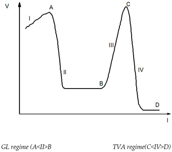 Figure 9. The two TVD regimes for different plasma parameters.
From the above so far presented description, one can derive the following characteristics of the TVD technology:
- -
- The film deposition must take place only in high vacuum conditions. If the rest gas pressure is not low enough, a stray auxiliary discharge can be ignited in the rest gas, and this will make the anode evaporation generation difficult and also it allows for the deposition material poisoning.
- -
- The cathode material must be tungsten, the material with the highest melting point which allows for high electron emission when heated to temperatures below the melting point. If one considers the low tungsten sputter yield and the low discharge currents in the GL regime, the net advantage of using a tungsten thermally heated cathode for high purity thin layers deposition becomes obvious.
- -
- The discharge currents can be varied in a large domain from some tens of milliamps to some hundreds of A as desired.
- -
- The anode evaporation is induced by electron bombardment of its surface which deliver their energies to the solid anode and induces its evaporation;
- -
- The deposited layer is formed in the condition of genuine ion bombardment with variable energy (of order of hundreds eV) as it will be shown later on;
- -
- The deposition rates can be varied in a very large domain since one can use both GLD and TVA regimes by discharge parameters variation;
In this case the anode voltage source must furnish both low current, high voltages and high current, low voltages. A simple possible electrical scheme also used by the authors of the present review article can be similar with that presented in Figure 10.
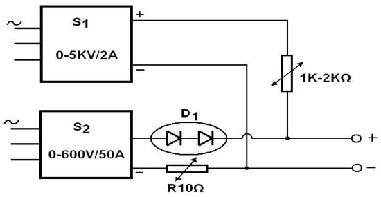
Figure 10.
S1 is a low current, high voltage source and S2 is a high current, low voltage source.
The above scheme can be expanded in a similar way with another source having higher current, lower voltage capabilities for arc discharges generation and high-speed deposition of layers for different industrial purposes.
The discharge variable parameters are the filament heating, the anode potential, the anode-cathode distance, cathode tilt with respect to the anode vertical (in the electron gun cathode case) and ballast resistance as well. All these parameters can be altered to monitor the deposition processes in a manner dictated by the real necessities.
5. Deposition Rates Obtained with Different Geometries
5.1. Electron Gun Geometry
In this section, the deposition rate dependence on filament heating current, discharge current, voltage and amount of electrical power introduced in plasma is highlighted as presented in [21,22].
To better understand the deposition phenomena, firstly it is worthwhile to present the general potential change along the anode-cathode distance as it resulted from many measurements carried out with an emission electrical probe and given in Figure 11.
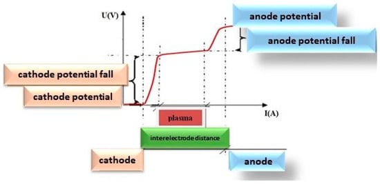
Figure 11.
Schematic dependence of electric potential in different points of anode-cathode gap.
As in other common gas discharge scenarios, a cathode potential jump forms in front of the cathode, accelerating electrons and ions towards the cathode. Then follows the plasma region which is a conducting medium, and the anode potential jump which accelerates electrons towards the anode, this way ensuring the necessary anode heating which in turn ensures maintaining a constant level of the anode evaporation because, otherwise, the discharge would extinguish due to the lack of “of gas”.
Indeed, the vapors present a special kind of gas since this “gas” condenses on the walls of the discharge chamber and on any other cold solid surface present within the deposition chamber (this way disappearing as a gas phase) and consequently, it must be continuously replenished.
An extensive study of the deposition behavior in TVD technology was carried out in copper vapor discharge [22].
Namely, the deposition rate, and the plasma ion energy dependences on discharge parameters when using TVD technology are to be presented below, especially when the electron gun cathode arrangement is used.
It is indeed very important to know how plasma parameters can influence the deposition rate to properly monitor and optimize the deposition process.
The main parameters that were changed during the deposition process are the cathode heating current, the discharge current and the positive high voltage applied on the anode. Another parameter influencing the deposition conditions is the anode-cathode distance which also can be changed during the process, but it will not be presented here.
Figure 12 gives some V-I characteristics measured in copper vapors for different cathode filament heating currents, namely 20 A, 22 A, 24 A and 26 A.
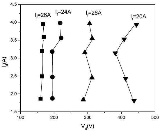
Figure 12.
V-I characteristics measured in copper vapors, for different filament heating currents values, If, marked on the figure.
One can immediately see that the discharge current, Id, increases practically at a constant discharge voltage, Vd, except for the curve for the lowest filament heating current, say If = 20 A.
In Figure 13, previously published by the authors in [22], the deposition rates against the power applied on the discharge, Pd, are plotted for different discharge currents, namely Id = 1.9 A, 2.5 A, 3.2 A, 3.6 A and 4 A, and for different cathode heating currents with the same values as in Figure 12.
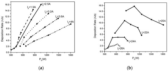
Figure 13.
(a) Deposition rate dependence on the discharge power for different discharge currents shown on the curves and (b) deposition rate dependence on the discharge power for different cathode heating currents, marked on the curves.
When measuring these data, a certain filament heating current was first chosen and by changing the anode potential, the discharge currents were measured together with the deposition rate on the probes.
Multiplying the voltage with the discharge current, the applied power was obtained, and the deposition rate was drawn as shown in Figure 13.
From these curves it is obvious that the deposition rate increases with the discharge power for the same discharge current but decreases when the discharge current increases (Figure 13a).
In Figure 13b, one can see that the deposition rate decreases when the cathode heating filament is increased, and for the same filament heating current, first the deposition rate increases with applied power, attains an apex and then decreases.
This apex is displaced to higher power values when the cathode heating current value is decreased.
Further on, a possible explanation of these special comportments will be presented.
Experimental measurements were taken for both deposition rates and plasma ion energies and for different plasma parameters shown above.
The deposition rates were recorded by a Cresington quartz balance while the ion energies were measured by a retarding field device mounted near the probes to be covered.
Let some general considerations be made concerning the behavior of the ion current variation against the positive potential applied on the collector of the ion energy measuring device.
It must be underlined here that the plasma electrons are impeded to arrive to the device by the plasma device (earthen) retarding potential and by a grid negatively charged, mounted in the face of the variable positive ion collector [23,24].
A typical recorded curve of the ion current coming from the plasma against the retarding potential applied on the collector of the ion energy measuring device is given in Figure 14.
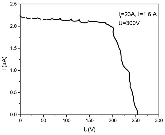
Figure 14.
Typical recorder curve for ion energy measurement. If is the filament heating current; Id = discharge current; applied positive potential on the anode = 300 V.
The ion current arriving to the device is practically constant until the retarding voltage begins to repel the lowest energy ions coming from the plasma. Here, some more considerations must be made.
Each ion gains energy within the plasma zone and gains additional energy when it escapes from that region on the direction to the grounded substrate, due to the potential difference between positive plasma and substrate potential of substrates and of the measuring on energy device. The last source of energy is the same for all the ions, while the first one (therefore within plasma) depends on the energy distribution of ions in the plasma.
For this reason, the collector current remains practically constant until the common energy gained by all the ions from the plasma-substrate potential difference is annihilated. From that potential, the number of plasma ions decreases until the last most energetic plasma ions can attain the positive ion collecting electrode, when the collected current becomes zero. The graphic derivative of the descending curve can furnish some information concerning the ion energy distribution in plasma.
According to Figure 14, one can see that the applied anode potential being 300 V, and the middle point of the descending curve appearing around 225 V, an electron accelerating anode fall of about 75 V is formed in front of the anode. This anode potential jump ensures the electron energy needed to evaporate the anode and maintain the plasma together with particle deposition during the discharge.
In the recorded curve, one can see that the plasma ion energy bombarding an earthen substrate is of the order of some hundreds of eV in the presented case (Figure 15).
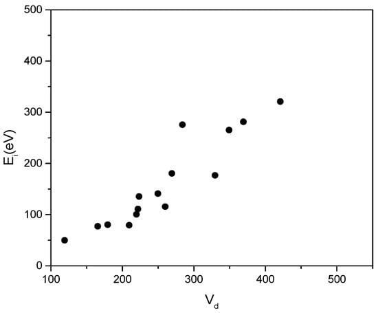
Figure 15.
The measured plasma ion energy dependence against the anode potential Vd.
If decreasing the cathode heating current, and trying to maintain the same discharge current, one must increase the anode potential to higher values. This draws up the plasma potential too and increases the ion energy available for a more efficient ion bombardment of the forming deposition.
It is now obvious how the energy of plasma ions which bombard the substrate could be changed, namely by simply changing the cathode heating current combined with positive anode potential changing when maintaining the same discharge current.
These curves could be considered as proof of the potential variation from the cathode (zero potential) to the anode where an electron accelerating anode fall is formed, as previously stated.
The dependence of plasma ions energy, Ei = eVp, on the anode potential, Vd, as experimentally inferred, is given in Figure 15.
The measurement of this dependence can be considered as being near a linear one.
The fact that the points are slightly scattered apart can be explained by the highly different conditions of plasma potential generation, which will be discussed further.
These measurements show that, when increasing the anode potential, the plasma potential increases too as if these two values were coupled with each other.
Therefore, it is to be supposed that when a more energetic ion flux is desired to come from the plasma region towards the substrate, one must increase the anode potential.
As mentioned above, a rapid potential variation jump is formed near the anode in order to maintain the anode material evaporation. The plasma is generated by electron-anode particle (toms or molecules) ionizing collisions.
Let Vp be the plasma potential near the anode and Vd the anode potential. Because the discharge current is exclusively carried by electrons, the energy introduced into the evaporating material can be written as:
where Id is the discharge current and Va = Vd − Vp.
Eev = Id(Vd − Vp) = IdVa
Here, it must be added that the electrons possess a thermal energy within the plasma which is of the order of an electron volt that is too low to generate the anode evaporation and to be considered.
This electric energy is balanced by anode thermal radiation, anode support thermal conduction and the anode particle evaporation (atoms or molecules of the solid material).
From these three energy loss mechanisms, the second one can be reduced to a negligible value by choosing the support of the anode as a thin tungsten wire (of order of one mm diameter) introduced in a hole drilled into the anode. In fact, there is a justified interest in lessening this kind of thermal loss as much as possible.
Therefore, one can write for energy balance in front of the anode:
where Id is the discharge current considered to be formed by the electron hitting the anode (the ions are repelled there), Va is the anode potential jump which accelerates the electrons towards the anode, N is the number of the particles evaporated from the anode per second, λ is the necessary energy to evaporate a particle from the anode material, β is constant containing the thermal emissivity of the composed anode material, anode radiating surface, S, and the Stefan–Boltzmann constant σ, and T is the absolute anode temperature [10].
IdVa = Nλ + ΒT4
Among the evaporated particles, the electron–particle collisions generate a certain number of ions.
Unlike the neutral particles (atoms or molecules depending on the nature of the evaporating material) which are uniformly spread around the anode (as in the case of usual thermal evaporation), the ions are supposed to be under the influence of the electric field present between the positive anode and earthen cathode.
When the discharge vacuum chamber has earthen metallic walls, these can attract the ions from the positive plasma too.
However, the distance from the anode to the metallic walls is by far longer than the distance to the cathode. Therefore, the ionized particles are expected to be directed preponderantly towards the cathode positioned nearby.
Near the cathode, the discharge current can be considered as given especially by the ions, the thermally emitted electrons being directed towards the plasma, where they are drastically multiplied and where their density approaches the ion one. The experimental evaluations show that the saturated thermal electron emission of the cathode is of the order of 0.1 A while the discharge currents used in this experiment are of the order of some amperes.
Considering that a DC discharge current, as in the TVD case, is constant along the discharge [16,25], the conclusion is that near the cathode the main component of the discharge current is ionic. Consequently, one can write for the number of the ions entering the cathode during a second:
ni = Id/e
Here, “e” is the elementary charge (the ions are preponderantly once ionized), Id is the discharge current and ni is the number of ions entering the cathode per second.
As mentioned above, the neutral evaporated particles might be considered uniformly distributed around the anode tip as they are not being influenced by the electrical fields.
There are no particle sources or sinks between the anode and the surface on which the Cresington gauge, which measures the deposition rate, is attached, hence the particle current is conserved, allowing us to write:
Here, a is a constant depending on deposition geometry (see also the Equation (14) together with the Figure 1), R is the distance from the anode to the deposition rate measuring gauge, ρ is the density of the depositing material, D is the deposition rate given by the gauge which represents the rate of film thickness growth per second, NA is Avogadro’s number, M is the atom gram weight of the deposited material and nev is the total number of the particles arriving within a second at the spherical surface on which the deposition rate measuring device is mounted.
Besides these particles, the discharge ions entering the cathode must be added to obtain the total number of particles evaporated per second from the anode. In other words, the evaporation particle was considered as follows: the neutral ones together with a small number of ions coming there are preponderantly measured by the quartz balance while the ionized particles are considered to arrive mostly towards the cathode where they are registered as the discharge current.
In this case, the total number of the particle leaving the anode per second, N, is given by adding Equation (7) with Equation (8), that is,
On the other hand, for a given anode temperature, the evaporation rate is given by Equation (12).
A more usual formula for the evaporation rate which uses the data given in the literature for different materials is [14]:
lg(N/(Nav S) = lg p + 22.546 − 0.5lg(MT)
Here, S is the anode surface, Nav is Avogadro’s number, p is vapor pressure in torr, T is temperature in K and M is molecular weight of the evaporating material.
It must be underlined that this formula is the same as the one described in Equation (12), having different measuring units.
The Equations (21) and (22) combine to give:
Here, the relation log p = log(NkT) = A − B/T was used in order to use the experimental data given for pressure in the literature with A and B being characteristic for every material [13].
From the Equations (18), (21) and (22), the following relation can be found out:
The measured values of D, R, a and Id together with universal constants contained in the second term of Equation (22) can provide the anode temperature, T, and therefore the term βT4 once the constant value, β, is known.
The β value is difficult to quantify in the experimental scenario since the anodic materials are very different and have complicated geometry; however, it can be evaluated for current purposes as follows.
Let a Va particular value be determined from the plasma potential Vp value, as given by the ion energy measuring device (by an electrical retarding field, as announced above). This one can be written as: Va = Vd − Vp.
Once this value is determined, using the corresponding N given by the first Equation (21) (which is furnished by the experimental measurements of the total particle number arrived within a unit time at the surface where the deposition rate device is posted, together with a discharge current that arrived at the cathode of the discharge), and the corresponding anode temperature T, given by the second Equation (24) (which is theoretically derived from thermo-dynamical equilibrium considerations via the Clausius–Clapeyron Equation (10)), the β constant can be deduced from the Equation (11) with that particular measured Va value.
Further, this value can be used in Equation (23) for determining all Va values corresponding to other plasma currents, deposition rates and anode temperatures. The plasma potential Vp values can be determined from these Va values simply by writing Vp = Vd − Va and plotted against the anode potential (discharge voltages).
Taking all this into account, we can use Formula (17) and calculate the plasma ion energy as a function of Vd. The newly obtained values are plotted on Figure 16, along with the experimentally measured values of the energy, versus the plasma potential measured by the electric field retarding device previously presented in Figure 15 and corresponds to the retarding potential that annihilates the maximum value of the plasma ion current.
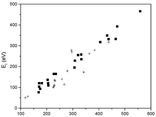
Figure 16.
The theoretical and experimental dependence of ion energy on the plasma potential. Black squares represent theoretical values while crosses represent the experimental ones.
This figure shows a good correlation between theoretical and experimental values, as well as the fact that both dependencies are linear.
Therefore, the plasma potential increases linearly with anode potential.
From the obtained data, it is interesting to plot the dependencies Va = f(Vd) and Vp = f(Vd) which can give an important inside look concerning the behavior of the TVD.
In Figure 17, one can see that the anode potential jump, Va, decreases for the same anode potential, Vd, when increasing the discharge current, Id. This seems to be logical because the greater the discharge current, the greater the electron number bombarding the anode and consequently the potential jump is allowed to decrease for a comparable anode heating energy to be obtained.
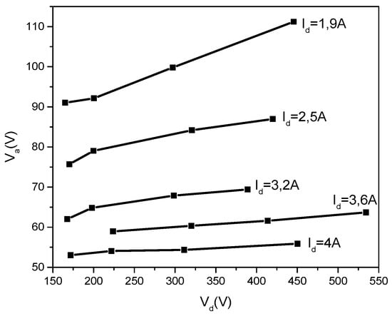
Figure 17.
Va = f(Vd) for different discharge currents (Id).
This anodic voltage jump, Va, seems to be almost constant against the discharge voltage, Vd, for the same discharge current value, especially for the higher discharge currents, while decreasing when Id increases.
On the other hand, taking a mean Va value for each curve and performing the corresponding IdVa products, one can see that all these are situated around the same power value, namely 200 W for all plots.
Considering that this power is responsible for anode heating, it is readily concluded that the anode temperature and therefore the corresponding evaporating rate is practically the same no matter what the discharge currents are.
This can suggest that the discharge current increases somehow similar to usual gas discharge cases when the gas pressure remains practically the same while increasing the glow discharge current.
Further on, one can conclude that when increasing the discharge current, that is, the evaporated particle ionization, a greater part of these evaporated particles are directed towards the cathode, forbidding them to travel towards the probes and to contribute to the deposition rate.
This explains the fact that the deposition rate decreases when the discharge current increases, as shown in the experimental data given in Figure 13a.
As for Figure 18, the Vp = f(Vd) dependencies, they are linear for the same discharge current, the higher current lines being situated above the lower ones.
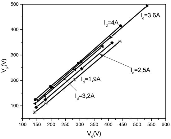
Figure 18.
Vp = f(Vd) for different discharge currents (Id).
Here, it must be underlined that in the TVD case, there is the possibility to vary three parameters during the measurements, namely the anode potential (Vd), the discharge currents (Id) and the filament heating current, (If).
Accordingly, Figure 18 shows for a given anode potential, Vd, the plasma potential, Vp, increases when the discharge current increases. This creates a greater cathode potential jump which ensures greater electron acceleration across this jump and consequently an increased particle ionization rate necessary for a higher discharge current.
A particularly strange behavior revealed the deposition rate dependence as plotted against the electrical power introduced into the plasma, for a fixed filament heating current, shown in Figure 13b.
First, the deposition rate increases when the filament heating current decreases. This can be explained by the fact that when If is higher, a lower power is necessary to be introduced into the plasma for the same Id currents and consequently, the deposition rate is lower too.
However, the curiosity appears when choosing a certain If, and plotting the deposition rate against the plasma power (as given by the product Vd Id). Firstly, the deposition rate increases with plasma power, attains a maximum and then decreases with increasing plasma power. That means that the deposition efficiency decreases.
Next, a tentative explanation for this strange dependence will be presented, considering that in case of these special discharges, the « gas » generation (the evaporated atoms) and its ionization are simultaneously produced by the same agent, while the electrons are both emitted from the heated cathode and generated by electron-atom collision.
From Equation (18), the partial power spent for atom evaporation within a second is given by:
λN = IdVa − βT4
From the above presented data, this value can be calculated and plotted against the corresponding discharge power, Pd = IdVd.
This graph is drawn in Figure 19.
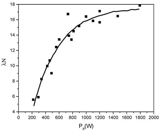
Figure 19.
Partial power λN = f(Pd) spent for evaporation during a second.
Figure 19 shows a rapid increase in the atom generation rate for lower discharge power, which decreases for higher discharge power.
On the other hand, from Equation (21) one can derive:
Here, in the second equation, the term Id = Pd/Vd, Vd was considered to be constant for a fixed filament heating current, as seen from the measured V-I characteristics.
The second Equation (24) represents the derivative of the deposition rate against the discharge power. The term dN/dPd can be inferred by graphically derivation on Figure 19. Plotting the dN/DPd = f(Pd) dependence together with (1/eVd) values taken for different filament heating currents, the discharge powers corresponding to the points of intersection of these curves gives the maximum positions of the deposition rate dependence against the discharge power for a fixed cathode heating current, If.
Indeed, one can readily see that for different cathode heating currents, the maximum value of the deposition rate, D, is obtained from the condition dN/dPd = 1/(eVd) which annihilates the derivative of D with respect to discharge power, Pd, as described in Figure 20.
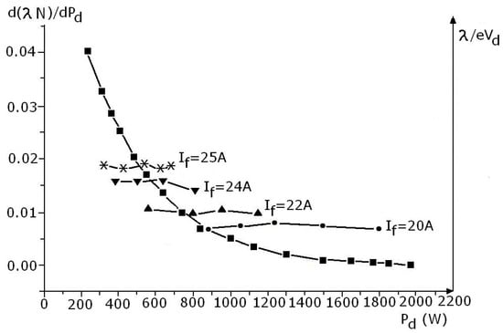
Figure 20.
d(λN)/dPd = f1 (Pd) and λ/eVd = f2(Pd).
It is readily seen that the maximum deposition rate is obtained at higher discharge power values for lower filament heating current values. That justifies the experimental dependencies shown in Figure 13b obtained for different filament heating currents.
All these highlight that there exists a competition between evaporation rate and ionization rate increase when increasing the discharge power:
For low discharge power, the evaporation rate increases faster with Pd, as compared with the ionization rate increasing and hence the deposition rate increases.
When Pd increases further, the evaporation rate increase diminishes while the ionization rate increases. This produces an increase in the discharge current and therefore a greater part of evaporated particles is evacuated through the electrodes and fails to arrive at the probes, mounted above the discharge gap. Finally, the net deposition rate decreases with increasing Pd, with the deposition efficiency decreasing.
Another important conclusion of the above given data can be the following one:
After heating the cathode filament and applying a high positive voltage to the anode, the thermo-emitted electrons are propelled towards the anode, they are heated, evaporation occurs and the discharge breaks down suddenly. Until the plasma occurrence, the ionizations are negligible, and all the electron energy is spent for evaporating anode material. After the breakdown, the evaporation is taken over by the plasma electrons accelerated across the anode fall Va. As suggested above, it seems that after the plasma breaking down, the evaporation rate of the anode material experiences a low increase, and the discharge behavior can be similar to that appearing in a usual gas. That means that the power spent on evaporation can be consider as being almost the same as that existent at the plasma initialization moment, at least for no very high discharge currents. In this case, the discharge power is spent mainly for electron vapor particles collisions of a different nature.
Now, let Vb be the breakdown voltage and Ib the corresponding initial discharge current which is mainly formed by the thermo-electrons elaborated by the cathode. If, after the breakdown, the evaporation rate remains the same, one can write:
where Va is the anode fall above mentioned which corresponds to the Id discharge current used during the deposition process.
VbIb ≈ VaId
Measuring the VbIb value just before the discharge ignition and the discharge current used during the deposition, the above relation can give the Va value. Knowing the anode potential, Vd, measured during the deposition process (for not very high discharge currents), the plasma potential is Vp = Vd − Va (see Figure 11), and the energy of the ions arriving to the earthen probe, eVp, can be deduced.
Experimental verification of these suppositions proved to be real and that gives the possibility to evaluate the ion energy, even when no such device is available due to different practical unfavorable situations.
As a conclusion of the above presented phenomena, one can say that this deposition method has three major independent parameters which can influence both the deposition rates and the genuine ion bombarding energy during the deposition process. These are the filament heating current, If, the anode potential, Vd, and the discharge current, Id.
The TVD technology possesses all the advantages of the thermal deposition as a possibility to localize the evaporation source and to use materials shaped as small pieces (even debris) but benefits the genuine ion energetic bombardment (of variable energies of the order of hundreds of eV) of the just-forming layers. When this energy is insufficient, the presence of ionized plasma allows the ions to be accelerated towards the substrate by applying a bias on it [26]. It is obvious that for thermal evaporation this facility is not applicable.
Moreover, while the thermal evaporation warms all quantity of evaporating material, the TVD method uses the electron bombardment of the material surface only, and sometimes it can allow for an energy saving or even can avoid the use of a crucible which can pollute the deposition purity, as will further be presented.
Indeed, when depositing tungsten, carbon, rhenium or other refractory materials, as further described when presenting the TVD technology for these materials, one can use the electronic bombardment of their surface only, to obtain a (superficial) suitable temperature for both evaporation and deposition with sufficient deposition rates, while the rest of the material is kept below its melting point.
In this case, the evaporation rate is not high, but this is in the benefit of deposition purity. Indeed, evaporation without a crucible avoids the possible contamination with the crucible material.
5.2. Ring Cathode Geometry
The new TVD arrangement uses a ring-like cathode filament, also made of tungsten and mounted just over the anode. The Whenelt type electric screen surrounds the filament this time, as shown in Figure 6.
As shown in Figure 6, the grounded filament allows the evaporated particles, no matter ions or neutrals, to travel towards the substrates intended to be covered. This time, the probes are mounted on the anode cathode direction and not at a tilt angle, as in the electron gun geometry assembly.
Therefore, the formed plasma and neutrals flow through the cathode and not through the anode, as in classical plasma jets devices (plasmatron, etc.).
When compared to the electron gun set-up, there is both a benefit and a disadvantage.
The advantage is that the ions are mostly directed towards the probes mounted above and which in turn helps in increasing the deposition rates with the power introduced into the plasma more efficiently because this time most of ions are directed towards the probe. Due to this fact, the deposition rate increases even when the discharge current increases.
In the electron gun arrangement, the deposition rate can decrease when the discharge currents increase, as presented above.
The drawback is that the position of grounded filament has a screening action with respect to the anode which can lower the energy of the ions bombarding the just-forming layer on the probes.
Opposite, in the electron gun geometry, the anode is completely open to the probes, the grounded cathode having a side position and this position introduces no screening between the anode and the probes.
Therefore, the amount of ions energy introduced into the bombarded probes is smaller in ring cathode configuration as compared with the case of the gun cathode.
Nevertheless, the ions can be independently accelerated or decelerated by applying a correspondent potential on the probes. These potentials proved out during different coating experiments carried out by the TVD technology to have a great importance, both for adherence and deposition structure.
The influence of ion bombardment on just forming deposition can be described broadly by the fact that ion energy leads to a local temperature increase, resulting in an increase in depositing particle mobility, which can improve particle arrangement in the new developing structure.
Additionally, when a deposited particle is loosely linked to the layer structure, it can be rapidly removed from that layer when hit by an energetic ion coming from the plasma.
This way, only the layer particles which are strongly connected with the neighboring ones will remain in the deposited structure after the action of plasma ion bombardment.
With other words, simultaneously with particle deposition, a slight sputtering effect takes place, and the layer structure is compacted and leveled at the same time.
6. Multiple Depositions by TVD Method
6.1. Simultaneous Depositions
As mentioned above, one of the advantages offered by TVD deposition technology is the possibility to easily obtain complex structured coatings due to its punctual character as an evaporation source.
Indeed, it is possible to obtain binary or ternary composed layers by igniting two or three simultaneous discharges with different discharge parameters, allowing for a large variety of previously programmed compositional depositions.
In Figure 21, an experimental arrangement used for a binary composite layer deposition is presented.
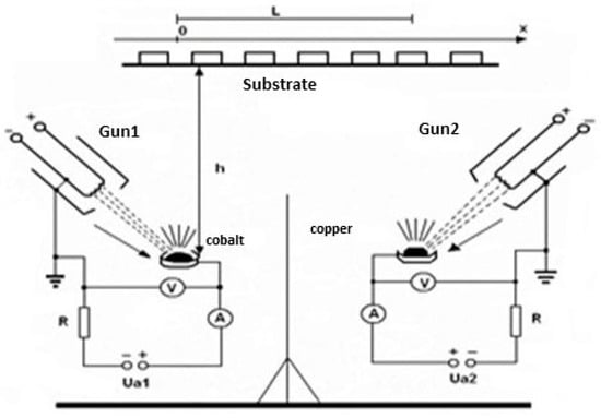
Figure 21.
Binary composite layer deposition scheme with two electron gun discharges.
Each separate discharge uses its own high voltage source and cathode electron gun as well. To remove the mutual electrical influence between the two discharges, an electrical grounded screen is mounted between the two discharges. The screen height must be sufficient as to exclude the charges from one of the discharges to arrive in the space of the other one but not so high as to impede the evaporated particles (ionized or not) to arrive at the probes to be covered.
Here, it must be underlined that in the case of cathode ring geometry, the Whenelt cylinder mounted around each filament ensures the electrical screening between the discharges too and makes the presence of an additional screen superfluous, as with the above presented one.
The best position for the probes is just above the two discharges aligned between them so that each probe can “see” both discharges as there would be no screen present in-between. An example is presented in Figure 21.
As previously described, the deposition rates depend on filament heating current, anode potential, discharge current or anode-cathode distance. Choosing these parameters for a discharge, the parameters for another discharge could be properly chosen to obtain a certain composition of the deposited layer.
Just as an example, in the following, a method to monitor the process aimed to obtain a certain binary composite deposition by using two independent simultaneous discharges will be described.
Let it be a binary composite material having one element labeled with “1” and the other one labeled with “2”.
Let the number of atoms of element “1” be ν1 and that of element “2” be ν2 in the deposited layer. The total number of atoms is given by ν = ν1 + ν2. Suppose the required atomic concentration of element ”1” be α = ν1/(ν2 + ν1) = ν1/ν.
Let the molecular weight and density of element ”1” be m1 and ρ1, respectively, while the corresponding values for element “2” be m2 and ρ2. Let us suppose that the volume occupied by a particle in the mixture is the same as that in the pure condition.
In pure conditions, the number of the particles “1” in a unit volume is n1 = ρ1/m1 while the same number for the element “2” is n2 = ρ2/m2. The corresponding volume occupied by a particle “1” is v1 = 1/n1 = m1/ρ1 and that occupied by the particle “2” is v2 = 1/n2 = m2/ρ2. If these volumes are conserved in the mixture too, then the partial volumes occupied within a unit volume of a given mixture by the particles “1” and “2” are:
ανm1/ρ1 and (1 − α) νm2/ρ2
Adding the two volumes, one obtains the unit volume, that is,
ανm1/ρ1 + (1 − α) νm2/ρ2 = 1
Therefore, the total number of particles (“1” and “2”) present in a unit volume when the particle concentration of element “1” must be α, and that of element “2”, 1 − α, is given by:
To verify the obtained expression, one can observe that when α = 1, only element “1” is present, ρam = ρ1, and when α = 0, when only the element “2” is present, ρam = ρ2, as it would be.
However, usually the quartz gauge measures the layer thickness and growth rate in length/s. There is a direct connection of this thickness growth and the rate of particle flux coming to the substrate which will be analyzed below.
Within a unit time, the quantity of substance “1” coming to the probes is given by (ν1/τ)m1 = Sρ1w1, where τ is the deposition time, ν1-the total number of kind “1” coming during this time to the receiving surface of area S, (quartz surface), w1 is the deposition rate of substance “1” (in length/s). Similarly for substance “2”, (ν2/τ)m2 = Sρ2 w2. However, in the desired mixture, one must have ν1/ν2 = α(1 − α). Finally, dividing these relations, one arrives at ν1/ν2 = [ρ1w1/(ρ2w2)] (m2/m1) = α/(1 − α).
Suppose one chooses to fix the parameters of the first discharge to ensure a deposition rate of the corresponding element “1”, say w1. In this case, to obtain the desired mixture in the deposited layer, the deposition rate of the second element must be given by the relation:
According to the data shown above, when a certain mixture compound having α/(1 − α) as the relative particle concentration must be deposited, the following steps ought to be followed:
One begins with the first element evaporation by introducing its density, ρ1, into the thickness measuring device and with adjusting the plasma parameters until the deposition rate, say w1, is obtained.
Maintaining the deposition parameters of the first discharge and replacing the density ρ1 with ρam, the second discharge is started-up, and its parameters are adjusted until the total deposition rate is given by
is obtained.
During the adjustment time of the two discharge parameters, the probe substrates are covered by a shutter. Finally, removing the shutter, the simultaneous deposition is continued with a rate given by (27), until the desired deposition thickness is attained.
The above considerations can be extended for three simultaneous depositions, considering the two-component mixture as a component, and taking the third component as a second one.
Usually, a more common and easier procedure can be carried out by mounting different separate probes along a line, as in Figure 22, and due to geometrical effects, a large and almost continuous compositional variation of deposition can be obtained from one probe to another one, at once. From all these probes, one can choose the desired one and use it for special applications.
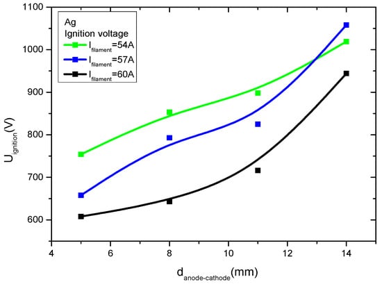
Figure 22.
The breakdown voltage against the cathode-anode distance for different cathode heating currents in silver vapor discharge case.
This might also be interesting when studying the concentration influence on a certain property of the binary structure.
6.2. Alternate Layers Deposition by TVD Technology
The TVD technology can be used to obtain multi-layered alternate depositions too.
The best geometry recommended to obtain the phenomena described below is the electron gun one. Considering Figure 21, let the central electrical screen be partially removed. In case of simultaneous depositions, this screen is used to ensure a complete separation of the two discharges and to allow each discharge to proceed independently from each other and to create a mixture on the substrates mounted above them.
The appropriate design which allows for alternate depositions to be obtained on the substrates is schematically presented in Figure 23. Here, a partial electrical screen is present and preferably, the reciprocal anodes positions are sufficiently near to one another as to facilitate the mutual influence of the two discharges. It is important to mention here that this distance, as a deposition parameter, can be chosen depending on the materials to be evaporated and deposited too.
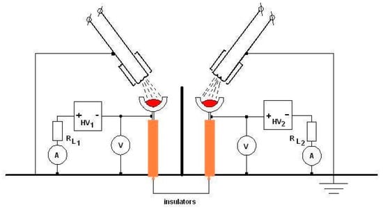
Figure 23.
Electron gun arrangement scheme for alternate deposition of two materials.
In principle, their vicinity is essential in order to facilitate the mutual influence of the two discharges which, as it will be shown below, will produce an automatic alternate burning of the two discharges which in turn, will ensure an alternate deposition of the two evaporated materials.
Let Equation (16) be written for each discharge with the corresponding distinguishing indexes, as follows:
E1 = Id,1Rl,1 + Vpl,1 for the first discharge, and
E2 = Id,2 Rl,2 +Vpl,2 for the second one
When considering the different V-I characteristics of a vacuum discharge for different cathode heating current and inter-electrode gaps, one can see a breakdown voltage dependence on these two parameters similar with those down TVD burning in silver vapor. Similar curves were obtained when, for the same cathode heating current, different V-I characteristics were plotted against the anode cathode distance.
It is seen that when the filament heating current is decreased and the cathode-anode distance is increased, the breakdown voltage increases (see also Section 7 below).
Additionally, the voltages E1, and E2 applied from the high voltage sources can influence the time elapsed from the starting moment of anode heating to the breakdown initiation. When these voltages are greater, the corresponding time intervals decrease and reverse.
Suppose the conditions are so that the first discharge is ignited, this depending on the evaporation rate of the corresponding material, on the anode-cathode distance, on the applied anode potential, on the cathode heating current and on the load resistance too.
From Equation (28), the plasma potential and therefore the anode potential, Vpl,1, given by,
is lowered due to the discharge current, Id,1 increases rapidly with the plasma ignition (usually from 50 mA up to 2 A). Meanwhile the second discharge being extinguished, its discharge current Id,2 is very low (50 mA) together with the load voltage, Rl,2Id,2. This maintains the second anode potential at the high values near the voltage applied from the second high voltage source, E2.
Vpl,1 = E1 − Id,1Rl,1
The electrons from the first discharge migrate towards the more positive second anode. As a result, the first discharge is partially depleted of electrons, its anode heating together with its evaporation rate diminishes and finally the first discharge stops.
On the contrary, the second anode, due to the first discharge electron contribution which is added to its proper electrons emitted by the second cathode and accelerated towards the higher positive potential still applied on the second anode (the discharge current is still low and therefore the voltage applied on the second discharge load is small), begins to evaporate with a greater intensity and the second discharge breaks down while the first one extinguishes.
The above-described phenomena are repeated with reversed roles.
This time, the first anode is at a high positive potential due to the fact that its discharge current is low, and the second anode potential is smaller due to the high voltage applied on the second load resistance (Rl,2Id,2).
Consequently, the first anode bombarded by the combined flux of electrons coming both from the first cathode and the second discharge still burning is intensely heated and the first discharge is again ignited while the second is extinguished due to the lack of electrons.
This way, the two discharges burn alternatively and so does the material deposition on the above mounted probes (substrates).
Many times, it is necessary to obtain a sandwich, having at least one layer with previously fixed thickness, as it will be described below.
That imposes that the burning time of the discharges needs to be monitored. This can be carried out by changing the two filament heating currents, If,1 and If,2, the anode potentials, E1 and E2, the load resistances, Rl,1 and Rl,2 and the anode-cathode distance (which can be performed from outside the reaction chamber even during the deposition). Finally, an electrical screen installed between the two discharges would have a significant influence on the time length of an ignited discharge by blocking electron transport to a lesser or greater extent. Indeed, when a good screening is present (as we used for mixture deposition) the two discharges can be maintained independently for as much time as the deposition is required. When using a grounded metal punched plate between the discharges, it will permit a partial transition of electrons and consequently, the plasma ignition will take place within different time intervals, that is, by this way one can influence the monolayer thickness deposited in a sandwich-type structure. This feature is critically important for the case of magneto-resistive multilayer structures deposited for magnetic memories.
Maybe some reactive components mounted in the external electrical circuitry would contribute to this monitoring and consequently to a more precise layer thickness variation.
For example, we must mention that for the alternate evaporation of copper and chromium, only one high voltage source was necessary with its positive potential simultaneously applied on the two anodes (E1 = E2) but having the other parameters different from each other.
Indeed, when using two separate high voltage sources (E1 ≠ E2), the possibility to obtain supplementary facilities for the alternate deposition of other thermally more different materials improves.
On a longer-term time, the two discharges will alternatively burn out by themselves with no external intervention.
This way, the deposition time for the alternate layers will be seriously shortened, considering that the electron cathode emission and anode heating do not completely cease during the extinguished periods of any of the two discharges.
The layer thicknesses can be adjusted by changing the above-mentioned deposition parameters until the quartz balance mounted near the probes shows the desired thickness value.
Moreover, when the burning frequency of the two discharges is sufficiently high and the deposition times are shorter, the layer thicknesses are small. In this case, a post deposition heating of the layers can contribute to a layer intermixing and to a binary mixture formation as an alternative method to the simultaneous mixture deposition previously described.
An additional advantage of the alternate deposition technique is that the anode is not continuously heated so that the bulk temperature of the anode can be maintained below the melting temperature while its surface may go over that temperature during the active deposition time.
This makes it possible to avoid the otherwise necessary crucible which can introduce contamination inside the depositions.
Finally, it should be noted that the electron gun configuration is more appropriate for TVD deposition since the two anodes can be conveniently put close to each other so their mutual influence may be preferable. The expected thicknesses of the deposited layers are in the range of a few nanometers which are very convenient for magneto-resistive layer deposition, as will be presented further on in this work.
With the ring cathode structure, this anode mutual influence is more difficult to realize due to natural screening introduced by Whenelt cylinders mounted around the ring cathodes.
However, if one removes the Whenelt, this ring arrangement can be used for multilayer deposition, too. It must be mentioned that TVD can be ignited even without the surrounding Whenelt, so it is possible to use this ring cathode structure for multilayer depositions.
However, as a general conclusion, one can say that the electron gun structure is more suited for the alternate layer structures (sandwich-type) deposition while the ring cathode structure is more suited for mixture deposition from the two or more vacuum discharges.
At the end of this section, it is worthwhile to contrast the TVD deposition technique with alternative deposition processes such as sputtering or arc discharge. Let the term of comparison be the structural quality of the deposited material.
As presented above, the inter-electrode space of thermionic vacuum discharge is mainly composed of three regions: the cathode fall region, plasma region and anode fall region. The anode fall is smaller than the cathode one and it is necessary to transfer enough energy to the electrons to maintain the anode material evaporation.
Let m be the electron mass, M the ion mass and ve-the electron speed after its acceleration in a certain ΔV voltage jump in one direction, and vi the corresponding ion speed after passing through the same voltage jump in the opposite direction. They both gain the same energy from the same voltage jump, namely eΔV. Consequently, mve2 = Mvi2 = eΔV, and the corresponding momentum ratio of the two particles is pe/pi = (m/M)1/2 which shows that the electron momentum gain is much smaller than the ion one.
Now, in case of the sputtering deposition procedure, the cathode particles are forced out from the cathode by the ion impact, which is mostly carried out by the argon ions generated in electrical discharges. The argon ion mass being 39.948 a.u. and the electron mass 5.5 × 10⁻⁴ a.u, one can see that the ion momentum is 7.3 × 10⁴ times greater than the electron one and consequently the above-mentioned momentum ratio (m/M)1/2 becomes 3.7 × 10⁻³. Moreover, the argon ion dimensions are much greater than those of the electron.
As a conclusion from all of this, it is obvious that an argon ion can extract both single particles and groups of many particles from the cathode material by ion-neutral momentum transferring collisions. These extracted particles of different dimensions are deposited on the substrates and have a bad influence on the deposited layer structure and purity.
In TVD technology the vapors are generated by electrons which are not able to transmit such a high momentum to the anode particles, but they transmit the same energy as the ions for the same potential difference. The energy transmitted by the electrons heats the anode material which evaporates atom by atom (as in the case of usual thermal evaporation) and so they condense on the substrate. However, in the TVD case, the as-deposited layer is continuously bombarded by energetic ions coming from the high potential of generated plasma near the high voltage anode. This way, one obtains in the TVD case a well-structured dense deposit with a good adhesion to the substrate [27,28].
On the other side, the TVD cathode is made of tungsten material which has one of the smallest sputtering yields of the known materials, as shown in the Figure 24 for the argon ion bombardment case. One can already see that the sputtering yield for tungsten is on the minimum of the right curve together with tantalum for all presented energy values of the ions.
Figure 24.
The sputtering yield of different materials by argon ions.
Additionally, the carbon sputtering yield is on the minimum of the left curve.
This ensures that very few tungsten atoms are extracted from the cathode by the plasma ion bombardment and, additionally, the Whenelt cylinder mounted around the tungsten filament impedes the sputtered tungsten atoms to arrive at the substrate position and to poison the deposition in the electron gun arrangement.
As was already said, the energetic ions coming from the positively charged plasma bombard the forming layer and have a remarkable influence on the deposited structure.
This effect, which is intense in TVD deposition, can be improved by a negative bias applied on the substrate. As an example of the bias applied on probes, Figure 25 presents the beryllium layer structure for different applied voltages on the substrate [26].
Figure 25.
SEM images for negative biased beryllium probe (a) and positive biased beryllium probe (b) deposited by TVD.
The improved structure of the beryllium deposit obtained in the event of a negative bias applied on the substrates (which accelerates the beryllium positive ions towards the probe) is easily apparent in Figure 25 when compared to the positive bias condition (which decreases the energy of ions and reduces their energy).
7. Magneto-Resistance
7.1. General Treatment
The phenomenon of magneto resistance analyzed here is that one of a pure quantum nature and consists in the variation of electrical resistance of a thin layer structure containing a magnetic material together with nonmagnetic materials, under the influence of an external magnetic field.
The magnetic material contains in its bulk structure, the magnetic domains characterized by the electron magnetic momentum oriented along a common line, due to the exchange forces (AUSTAUSCH) [29,30,31,32] of pure quantum nature. These forces, present in the ferromagnetic metals, makes it possible that the electrons with the energy near the Fermi level have the same spin orientation due to the complete unbalanced energy level density available for spin up and spin down electrons.
That means that in the following presentation, there is no connection between classical Larmor precession influence on electron movement into the deposited thin layer structure.
One of the most suitable deposition methods which can be used to obtain such magneto resistive layers is the TVD method, both for depositions of sandwich-type of structures or of mixtures of magnetic material with nonmagnetic materials, which have magneto resistive characteristics.
Further, the quantum effects contributing to magneto resistance will be treated as simple as the phenomena that occur when diatomic molecules are formed [33]. This is appreciated to be sufficient from the point of view of a plasma specialist which conducts the deposition process by thermionic vacuum discharge into a vapor atmosphere.
Indeed, for a solid-state physicist, it will not be sufficient, but the following works are recommended on the subject [6,34,35,36,37].
The following thin layer structures will be presented:
- a.
- Alternate magnetic-nonmagnetic metallic (sandwich-like) multi-layered structures—so called GMR (giant magneto resistance) structures [38,39,40,41,42,43]:
- b.
- Multi-layered combined structures similar with the previous one but for this instance, the nonmagnetic metal is replaced by an insulator, the so named TMR (tunnel magneto resistance) structures [40].
Both these structures can be obtained by separate ignited discharges or by alternately self-ignited discharges, as described above.
- c.
- Granular, GMR structures where the magnetic metal is uniformly distributed throughout the non-magnetic metal crystal net [44,45];
- d.
- Granular, TMR structures where the nonmagnetic crystal net of the previous structure is replaced by an insulator [46,47];
- e.
- Combined ternary multi-layered structures having a nonmagnetic metal or an insulator used as intermediate layers between two magnetic metal layers;
- f.
- Combined ternary uniform mixtures with magnetic material uniformly distributed in a non-magnetic metal and insulator binary mixture;
- g.
- Different combinations between e and f structures.
The c, d, e, f and g structures can be obtained by temporarily separated vacuum discharges, or by two or three simultaneously ignited discharges.
7.2. GMR Type Depositions
7.2.1. Multi-Layered
Schematically, this type of structure is given in Figure 26, where only the basic structure is represented, the real structures being made of multiple repetitions of this base.
Figure 26.
Sketch of a multilayer basic structure deposition.
For the following theoretical presentation, Figure 27 is taken, which presents a basic structure for GMR layer depositions.
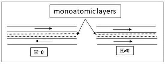
Figure 27.
The magnetic material can be iron, cobalt, nickel, permalloy, etc., deposited alternatively with nonmagnetic metal layers, as copper, silver, gold, platinum, etc.
In this figure, two situations are presented together with the magnetic domains optimally oriented in the absence and in the presence of an external magnetic field.
Between the two magnetic layers, two non-magnetic conductor mono layers are represented by two atomic strings designated as black dots.
The magnetic reciprocal domain orientations are indicated by arrows and the most favorable orientation, from the point of view of magneto resistance, is that when it is anti-parallel, in the absence of the magnetic field, and which becomes parallel in the presence of an external magnetic field.
To obtain an enhanced magneto-resistive effect, this structure is multiplied by several tens in the final magneto-resistive structure. In this case, each group of magnetic-non-magnetic layers builds up its contribution to the electrical resistance changes in the presence of the magnetic field [32,48,49].
Another condition imposed to be fulfilled for a good magneto-resistive effect, is that the anti-parallel domain orientation must be recovered, once the magnetic field is removed. Otherwise, regardless of the external magnetic field, the domains remain parallel oriented, and no variation will appear as in a pure magnetized ferro-magnet.
That means that the magnetic coupling of the domains from the two magnetic layers must not be too strong so as to allow for the exchange of magnetic forces to bring back the anti-parallel orientation in the absence of the external magnetic field. That means that the thickness of the intermediary nonmagnetic layer must be sufficiently high. On the other hand, this thickness must not be too high because, in this case, any interaction between the ferromagnetic layers will disappear.
Intuitively, the greater the non-magnetic layer thickness is, the less the mutual magnetic coupling between the two magnetic layers is.
Certainly, the thermal effects contribute to the regular magnetic alignment disturbance. Therefore, the magneto-resistive effect will be smaller at higher temperatures and conversely at lower temperatures.
The magnetic coupling of domains from the two magnetic layers is made through the conduction electrons present in the nonmagnetic metal [26,50]. When two magnetic layers separated by a nonmagnetic metal are deposited, it is of interest that the majority of magnetic domains present in one of the magnetic layers will be antiparallel oriented with domains present in the other magnetic layer. This arrangement can be facilitated or impeded by the nonmagnetic layer; hence, thickness will be playing a decisive role. A possible explanation of this phenomenon will be presented now.
Let two ions be considered which are chemically linked by two common outer electrons (covalent or metallic-type bond).
The two electrons will be labelled “1” and “2”. If the quantum state for the electron “1” is described by the assemble of quantum numbers labelled q1, and its position is designated by r1, the characteristic quantum wave function will be written as Ψq1 (r1). In this case, the characteristic quantum wave function for the electron “2” situated in the position r2 and occupying the quantum state q2, will be denoted by Ψq2(r2).
The quantum probability to find the electron “1” in position r1 with quantum numbers, q1, and the electron “2” in position r2 with quantum numbers, q2, is described by the square of the product.
Ψq1 (r1). Ψq2(r2) (because the total probability is composed by “and”) [47]).
However, the two space identical electrons can be interchanged, and the corresponding wave function would be given in this case by the following product Ψq2 (r1). Ψq1(r2), this function representing a solution with the same system of quantum numbers (proper values).
Finally, the wave function for the two electrons may be written as a linear combination of these two (which is also a solution of the linear Schrodinger equation):
Ψ(r1,r2) = Ψq1 (r1).Ψq2(r2) + αΨq2 (r1).Ψq1(r2)
Here, α is an adjustable parameter that will be chosen as to minimize the energy of the considered system [29,33].
Let H be the total Hamiltonian of the system and:
Here, H11 and H22 are the quantum energies corresponding to the case when the electrons are situated near their ions, while H12 = H21 are the exchange energies, that considers the case when the two electrons mutually interchange with each other, and γ is the normalization factor.
The total energy of the system is given by:
E = Min α [(1 + α2)H11 + 2 α H12]/[1 + α 2 + 2 α γ)
Let
As mentioned above, the value of the α parameter is found from the condition of minimal energy which is obtained by taking the derivative of the relation (31) with respect to α and by equaling the obtained expression with zero.
As a result, one obtains:
(1 − α 2)(H12 − γH11) = 0 → α = ±1
As it will be shown below, the qualitative dependence E = f(α) as presented in Figure 28, can be deemed to be as that presented in the Figure 24 for two cases (vis. when exchange energy, H12 < 0 and when H12 > 0):
Figure 28.
The quantum energy dependence against parameter α. (a) H12 < 0. (b) H12 > 0.
In order to find out the minimum and maximum of the function E = f(α), one can study the sign of the function d2f(α)/dα2 in the points where the first derivative is zero. Alternatively, one can observe that f(−∞) = f(0) = f(+∞) = H11, f(−1) = (H11 − H12)/(1 − γ) and f(+1) = (H11 + H12)/(1 + γ).
Here, two cases appear:
- (a).
- H12 < 0
In this case, the energy value (E) starts from H11, for α at −∞, becomes (H11 − H12)/(1 − γ) > H11 at α = −1, then becomes H11 at α = 0 again, decreases to value (H11 + H12)/(1 + γ) < H11 for α = +1 and finally increases to H11 for α tending to +∞. The corresponding graph is shown in Figure 28a.
In conclusion, when H12 < 0, the favored energy value is obtained when α = +1. As a result, the wave function in this case will be given by:
Ψ(r1,r2)= Ψq1 (r1).Ψq2(r2) + Ψq2 (r1).Ψq1(r2)
Additionally, this represents a symmetric wave function with respect to electron permutation.
- (b).
- H12 > 0
In this case, the energy value starts again from H11 at −∞, passes through the same formally expressed values as before, but with absolute values inversed relative to H11. That means that in point −1, the function will present a minimum while in point +1, it will present a maximum, as shown in the Figure 28b.
The favored energy in this case is obtained for α = −1 and the corresponding wave function will be:
which represents an anti-symmetric wave function relative to electron permutation.
Ψ(r1,r2) = Ψq1 (r1).Ψq2(r2)−Ψq2 (r1).Ψq1(r2)
Since the electron spin value is known to be ½ [51], the total quantum function builds up from the product of wave function with the spin function and it must be anti-symmetric.
However, in the first case, the wave function being a symmetrical one, it determines the spin function to be anti-symmetric and therefore the spin orientation to be anti-parallel (↑↓).
For the case (b), similar considerations lead to the conclusion that the two spins are parallel oriented (↑↑).
Assuming a first ferromagnetic layer is deposited. As presented in case (b), the exchange forces build-up in the layer and the magnetic domains are with parallel orientation. The parallel orientation of the magnetic domains can be enhanced when applying a magnetic field during the deposition process.
Let the next deposited monolayer be made of a nonmagnetic conductor metal. Consider an atom from this second layer which is bonded to an atom of the magnetic layer. To form a covalent bond, the two electrons put together in this manner must be predominately located between the two atoms (one from the magnetic layer, the other from the conducting layer). The wave space function that describes a higher electron density between the atoms and therefore, a stronger electric force between the two adjacent ions, is the symmetric one. If the space function describing the two electrons is symmetric, then the spin function must be anti-symmetric, that is, the spins of the two electrons are anti-parallel oriented.
Continuing with such reasoning, an atom from the next (second) nonmagnetic monolayer deposited over the previously (first) considered nonmagnetic one, will have the electron with a spin anti-parallel oriented relative to the precedent electron from the first nonmagnetic monolayer, and parallel oriented relative to the spin of the electron from the magnetic layer.
If the next layer will be a ferromagnetic one, the spin of its bounding electron will be anti-parallel with the spin of the electron from the second non-magnetic monolayer (situated beneath him) parallel with the corresponding spin of the first nonmagnetic layer and anti-parallel with respective to the spin from the base ferromagnetic layer.
Therefore, the preferred relative domain orientation in the two ferromagnetic layers is anti-parallel, as presented in the first layer arrangement presented schematically in Figure 27.
Applying an external magnetic field produces an alignment of all domains along its direction, while removing the external magnetic field will rearrange the domains in the anti-parallel orientation due to minimum energy above the presented condition.
It is easily seen that if one more nonmagnetic monolayer is additionally deposited between the ferromagnetic layers, the reciprocal orientation of the domains from the two magnetic layers will be a parallel one. In this case a possible applied magnetic field will produce no changes in the parallel orientation of the domains and no magneto-resistive effect would appear.
Now, if another nonmagnetic monolayer is added (fourth in this case), the anti-parallel orientation of the magnetic domains in the two ferro-magnetic ones is build up in the absence of the external magnetic field.
An even number of the nonmagnetic monolayers will favor an anti-parallel domain orientation within the two ferromagnetic layers (for no external magnetic field) while an odd number of the nonmagnetic monolayers will favor a parallel mutual orientation of the magnetic domains from the two ferromagnetic layers.
On the other hand, the more nonmagnetic layers are present between the two ferromagnetic layers, the less the magnetic coupling between the magnetic domains is.
These considerations will be used below for further interpretations on the magneto-resistance behavior. As a necessary result, a damped oscillation of GMR effect will appear as a function of the nonmagnetic thickness [52].
Now imagine these three layers discussed earlier and an electric current flowing through them. The electrons of this current will suffer collisions with electrons present in the magnetic domains. The spin orientation of two such electrons will be parallel or antiparallel. As is known, the differential cross section is given by the squared absolute value of quantum collision amplitude, |f(θ)|2 [7,51,53]. However, due to the quantum symmetry conditions one must consider two different wave functions, namely [25]:
where the plus sign denotes a symmetrical wave function (anti-parallel spins) while the minus sign signifies an anti-symmetric wave function (parallel spins).
f(θ,φ)s-a = C[f(θ,φ) ± f(π−θ,ϕ+π)]
The differential collision cross section being given by the expression σ = ׀f(θ,φ)׀2 so that the following expressions of the collision cross section for the anti-symmetric and symmetric case will be obtained:
σa = ׀f(θ,φ) − f(π − θ, φ + π)׀2 and σs = ׀f(θ,φ) + f(π − θ, φ + π)׀2
From these expressions, one can see that when the two electrons have parallel spins and consequently an anti-symmetric space wave function, their collision cross section is different from that when an encounter of two electrons with anti-parallel spins (symmetric wave function) takes place. Two situations could appear:
- a.
- Both functions have the same sign, in which case σs > σa. Then the spin anti-parallel case will have a greater collision cross section and a greater electrical resistance will appear;
- b.
- The two functions have different signs when σs < σa and the spin parallel case will have a greater collision cross section and a greater electrical resistance.
The electric current flowing through the structure can be considered as being composed of two parallel currents, one with the “spin-up” electrons and the other with the “spin-down” electrons. The conduction electrons collide with the electrons ‘localized’ in the magnetic domains of the ferro magnets.
Let the case when the ‘localized’ spins from the two ferromagnetic layers (one above the conducting nonmagnetic layer and other beneath it) are mutually anti-parallel oriented be considered, in the case of a zero external magnetic field. These two magnetic layers can be of the same material or from different magnetic materials. That implies that in the first case, the quantum collision amplitude of the localized electrons is the same for both magnetic materials or it may have different signs in the second case. We will only consider the case when the magnetic material is the same in both magnetic layers and combined with the case (a) mentioned above. A complete analysis of different combinations can reveal the possibility of inverse GMR existence when the structure resistance is less in the case of antiparallel magnetic domains orientation.
In order to fix the ideas, let the first magnetic layer have “up” ‘localized’ spins and the second one “down” ‘localized’ spins.
Flowing through the first ferromagnetic layer, one half part of conduction current having a “down” spin orientation (that is an anti-symmetric spin function), its corresponding wave function is forced to be symmetric and the case (a) is met and will suffer an electrical resistance increased by an amount, δr, while in the second ferro-magnet with another spin orientation will suffer a decreased electrical resistance by the same amount δr, the wave function being anti-symmetric. Therefore, the resistance opposed by the first layer will be R0 + δr, while the second ferro magnet will have the resistance R0 − δr.
For another component of the conducting current, having “up” spin orientations of the conducting electrons, the situation is opposite and the resistance of the first layer will be R0 − δr, while that of the second one will be R0+ δr.
As a result, the total resistance sensed by one half of conducting electron current is 2R0 and the same value will be sensed by other components of the conduction current, that is, 2R0.
As they flow in parallel, the equivalent total resistance R↑↓ results from 1/R↑↓ = 1/2R0 + 1/2R0 = 1/R0 → R↑↓ = R0. This is the equivalent resistance opposed by the anti-parallel orientation of the ferromagnetic domains-zero magnetic field case of the structure.
When the structure is subjected to an external magnetic field whose orientation coincides with that of the first magnetic layer, the magnetic domains of the second magnetic layer will be parallel aligned along this direction and all the magnetic domains become parallel.
In this case, that half of conduction electron current with the same spin orientation will face a decreased electric resistance in both of the magnetic layers. The corresponding resistance will be R0 − δr + R0 − δr = 2R0 − 2 δr.
However, another half of the electron conduction current (with the opposite spin orientation) will flow against the resistance R0 + δr + R0 + δr = 2R0 + 2 δr.
The equivalent electrical resistance in this case (in the presence of an external magnetic field) will be given by
1/R↑↑ = 1/(2R0 − 2δr) + 1/(2R0 + 2δr) → R↑↑= R0 − (δr)2/R0
The so-named magneto resistive effect is usually described by different authors, by one of the following relations:
(R↑↑ − R↑↓)/R↑↑ = −(δr)2/(R02 − δr2) or (R↑↑ − R↑↓)/R↑↓ = −(δr)2/R02
From the two definitions, the first one has the advantage of being more optimistic but without any real consequence. Therefore, the oversimplified behavior of the current flow through the GMR structure was described, but a more exact treatment of the problem could be found elsewhere [36,54].
In the case of two different magnetic materials with wave functions of different signs, one can find an inverse GMR effect by similar considerations. Indeed, changing the sign of one wave function implies a change of the corresponding spin orientation too in order to maintain the electric effect. Or that implies that a decreased electric resistance will appear in the antiparallel magnetic domain case (zero magnetic field) and an increased resistance will appear in the parallel magnetic domain orientation (magnetic field difference of zero) that is an inversed GMR effect.
Another way to describe the electron flow through GMR is to consider the band structure of deposited layers [52].
The electron conductivity σ = 1/ρ (ρ is the resistivity) of a metal is proportional with the number of electrons having the energy equal with the Fermi level, Ef [3]. This number is determined by the density of allowed states existing there, Df. Therefore, the metal conductivity could be considered as proportional to the energy level density near its Fermi level.
In a nonmagnetic metal, the energy densities, D, for both spin directions can be represented by the central graph of Figure 29, where the densities for the two spin orientations are completely balanced. Instead, for a magnetic metal at the Fermi level, a completely unbalance density appears for the two spin orientations, due to the exchange energy that lifts up the spin ‘up’ density, as shown on the graphs posted on the left and right side of the nonmagnetic graph.
Figure 29.
Energy level density distribution in magnetic and nonmagnetic metals together with corresponding conductivities for the two magnetization cases. Reprinted with permission from Ref. [52]. © 2008, Indian Academy of Sciences, Bengaluru.
In Figure 29, the first graph from the first line at the Fermi level, it can be seen that the spin up electrons are more numerous while the spin down ones are absent. The same situation is present on the right graph of the same line, corresponding to the case of parallel magnetizations of the magnetic layers present in the GMR structure. The central graph shows the situation for the nonmagnetic layer.
The ‘up’ electrons from the Fermi level of the left magnet can jump from this level to the corresponding ‘up’ nonmagnetic level and from there to the ‘up’ level of the second magnet where they find sufficient levels to fall on.
However, there are none (or few) “down” electrons in the left magnet and this annihilates the “down” current from the start.
In this case a high current flowing through the structure is present, ensured by the “up electrons.
On the second line, the anti-parallel magnetization case is presented (no external magnetic field).
Here, the ‘down’ electrons near the Fermi level on the left graph are scarce, as before, so they could not contribute to the current. Instead, the ‘up’ electrons from the same graph can jump to the ‘up’ nonmagnetic levels of the central non magnet but they could not go any further because they will not find levels near the Fermi energy in the second anti-parallel magnet, due to the anti-parallel magnetization. Therefore, in the case of anti-parallel domain orientation, both current components are impeded from flowing through the structure.
Once more, the parallel magnetization ensures a low resistivity due the ‘up’ short, and the anti-parallel magnetization cannot allow a significant current flowing through the structure.
All these considerations are valid if the so named spin flip mean distance is greater than the thickness of the nonmagnetic layer because only then does a spin ‘up’ (or ‘down’) electron starting from the left magnet come with the same spin orientation at the right magnet.
But what would happen if this spin flip-flop distance is less that the nonmagnetic spacer thickness? Then, a spin ‘up’ electron will start from the first ferromagnetic layer and will arrive to the second ferromagnetic as a spin ‘down’ electron and will find a great number of levels for an anti-parallel magnet orientation (when the magnetic field is zero) and few numbers of levels for a parallel magnet orientation (when the magnetic field is present). That means that the conduction is greater for a zero magnetic field and smaller in the presence of the external magnetic field, that is, a negative GMR effect will appear.
To obtain the best magneto-resistive effect, the zero magnetic field domain orientation in the two ferromagnetic layers must be as anti-parallel oriented as possible while in the presence of a magnetic field, it must be as parallel oriented along the magnetic field direction as possible.
If the zero-field orientation is parallel, then a non-magneto-resistive effect will appear, as seen from Equation (32) too.
The temperature influence is of course detrimental, and the temperature decrease will improve the magneto-resistive effect.
Multi-ferromagnetic-nonmagnetic layer combinations additionally increase the magneto-resistive effect.
As mentioned above, the thickness of the nonmagnetic conducting metal contributes to the transition from the anti-parallel zero magnetic field coupling to parallel magnetic field coupling of the domains from the ferromagnetic layers. This also influences the magnitude of the magneto-resistive effect. In the case of parallel zero field orientation, the effect is zero while in the case of anti-parallel zero field orientation, the effect is maxim.
The multilayer (sandwich-type) structured depositions can be easily obtained when using TVD technology, by alternate plasma ignition in the desired material vapors [12,42]. However, the necessary time for deposition is long enough since a lot of time is lost during the off-deposition periods when the material needs to be reheated, re-evaporated and re-deposited from the burning discharge. Usually, the off-deposition time is greater than the deposition one. Therefore, the waste time is large, considering that many layers (habitually some tens of layers) must be deposited in order to obtain a greater magneto-resistive effect.
Instead, alternate self-adjusting discharges with electron gun geometry, as described previously, can allow for a lot of time shortages.
Indeed, in this case, the anodes are maintained at a higher temperature since the filament heating together with anode potentials are all the time maintained on from the sources, the plasma being ignited and extinguished by self-regulating alternate anode potentials.
It is interesting to mention here that the GMR effect of multilayer type structure has different values if the electric current is forced to travel along the deposition (CIP = current in plan) or perpendicular to it (CPP = current perpendicular on plan).
The GMR effect value is greater in CPP geometry as in the CIP one because the current is forced to travel all the layers but the practical realization of CPP structure is more difficult, and the resistance is lower than that for CIP.
7.2.2. Granular GMR
The composite layer is made now of a mixture of magnetic metal (Fe or Ni or Co, etc.) uniformly distributed within the network of a conducting non-magnetic metal (Cu or Ag or Au, etc.).
The TVD technology is very suitable for such depositions too. The coating process is carried out in a high vacuum, from two independent simultaneously burning vacuum discharges, having an electrical screen mounted between the anodes, as previously presented in Section 5 when discussing the simultaneous discharges [48,49].
For scientific studies concerning the influence of the mutual metal composition over the magneto-resistance effect, this technology is warmly recommended due to the fact that the sources are punctual, and the deposition rate depends on the source-substrate probe distance and substrate orientation, as in case of thermal evaporation.
By mounting the probes between the sources, a high variety of deposition concentrations is obtained at once.
Both the electron gun and the cathode ring arrangements can be used for the same purposes. In the cathode ring arrangement, considering that the surrounding earthen Whenelt cylinders ensure the necessary electrical screening between the discharges, there, the presence of any electrical screen between the discharges becomes futile.
The magnetic metal, having a granulate form, must be distributed as uniformly as possible throughout the nonmagnetic material. The TVD technology, which uses electron bombardment (and not ions as in the sputtering case) as a source of anode heating and plasma generation, ensures a very fine (almost atomic) uniform distribution of the magnetic atoms within the non-magnetic metallic network, as previously mentioned.
This facility will contribute to obtaining certain desired qualities of the magneto-resistive structure, as will be discussed further.
It is worthwhile to make a comparison between the multilayer structured depositions and those with granular structure to derive some general data concerning the behavior of them under the action of external magnetic field.
The function of a non-magnetic conducting layer from the sandwich-like structure is now overtaken by the distance between two adjacent magnetic domains filled by the nonmagnetic material.
Indeed, if the magnetic particle density is too high, then this distance is too small, the mutual interaction between them is too high and the external magnetic field fails to change the domain orientation in its presence, as in the case when the non-magnetic conducting layer thickness is too thin.
On the contrary, when the magnetic material concentration is too low, the distance between two adjacent domains is too high and the exchange forces are ineffective. Moreover, when the magnetic material concentration is too low, the magnetic domain presence is too scarce, their total GMR effect is too weak and consequently the magneto resistive effect is too low.
As a result, there exists an optimum magnetic material concentration for a maximum magnetic magneto resistive effect, and this concentration is around 30%.
The dimensions of the magnetic domains have a great importance too. The best situation for some applications is when the magnetic particle dimensions are of the order of one atom and are uniformly distributed in the bulk structure of the magneto resistive layer.
During the deposition process carried out by the TVD technology, the substrates are heated up to some hundred Celsius degrees (due to anode radiation combined with the plasma particle action) which is an advantage in comparison with other deposition method. When this heating action is not sufficient, a post deposition thermal treatment is crucial to coagulate the magnetic particles to form magnetic domains having optimum dimensions.
It is of special interest to obtain a very narrow distribution of the domain dimensions.
As given in the literature, the domain diameters distribution when they are considered spheres, is given by [55].
where β is the mean deviation of a diameter, D, with respect to the mean magnetic grain diameter, D0, and A is given by the relation , corresponding to the distribution normalization, c being the diameter of a singular magnetic atom (the minimum particulate dimension of a domain).
From the above given considerations, one can infer that, if the deposition can be made of magnetic atoms uniformly distributed in space all over the network of the nonmagnetic metal and with a proper concentration, a proper post-deposition thermal treatment can produce magnetic domains with a very thin diameter distribution around the mean diameter, D0 value.
As a result, the orientation for the great majority of magnetic domains, under the influence of an external magnetic field, will be produced for a unique value of the external field and the GMR effect plotted against the magnetic field will have steep slopes on the wings, as it will be presented below.
If these dimensions are largely spread around D0, (great β, value) their orientation along the external field will be produced for different magnetic field intensities and the plot of the GMR effect against the magnetic field will have slowly decreasing slopes.
The width of these dependencies will be broader or thinner depending on the softness of the magnetic material embedded in the non-magnetic conducting material.
Examples of such dependencies will be presented in the section dedicated to applications of the TVD technology.
7.3. TMR Type Depositions
In TMR (tunnel magneto resistance) depositions, the nonmagnetic conducting metal is replaced by an insulator and the electric current is forced to penetrate the insulator by the quantum tunnelling effect [40,46,47].
In this case, the electrical resistance of the structure is much greater than in the GMR cases and consequently this structure works with much lower currents.
This behavior makes it possible to use TMR in non-volatile magnetic memories.
There are many insulating materials which can be deposited by the TVD method, even if it uses dc electrical discharges for deposition. The possible insulating materials to be deposited by this technology are those which become conductive at high temperature used for their evaporation.
When this will not be the case, as for example the aluminum oxide (alumina) deposition, a thin aluminum layer is first deposited by TVD technology which can be further oxidized by a glow discharge in an oxygen atmosphere. The advantage is that the thicknesses for TMR structures are of the order of nanometers.
7.3.1. Multilayer TMR
A simple quantum description of the phenomenon will be further presented to obtain some basic explanation of its behavior in an external magnetic field.
To begin with, let it be considered the simplest potential barrier built up by an insulator deposited between two magnetic metal layers. The form of this barrier is sketched in Figure 30.
Figure 30.
Potential barrier in a TMR layer.
The corresponding Schrodinger equation for this simple barrier is:
The solutions of this equation for the three regions are [51]:
k12 = k32 = 2mE/2; k22 = 2m(U0-E)/2, E = electron energy.
The A, B, C, D and F constants are obtained when equalizing the functions and their derivatives at the points 0 and l.
The probability for an electron to pass through the electrical barrier, that is the quantum barrier transparency, is given by:
The interesting case is when the electron energy, E, is much smaller than the potential height, U0.
In this case, sh(k2l) ≈ exp(k2l). In this approximation, the barrier transparency becomes:
From this expression one can see that the barrier transparency exponentially decreases with the barrier height (U0) and barrier extension (l) and increases with the electron energy.
For this reason, the insulator layer thickness must be thin enough to obtain a sufficient electron current, but not too thin because it will produce a strong magnetic coupling of the two adjacent magnetic metal layers. This would diminish the influence of the external magnetic field.
The external magnetic field efficiency is appreciated after the magnitude of the so denoted TMR effect, ηtmr, described by the relation:
where R0 is the resistance for the zero magnetic field and Rh is the resistance in the presence of the external magnetic field, as in the GMR case.
The electric current passing through the barrier is proportional with this transparency, with the energy states densities around the Fermi level existent at the magnetic metal-insulator contact surfaces, and with the electron distribution function on these energetic levels (Fermi-like distribution).
The energy-space transparency makes no difference between spin “up” electrons and spin “down” electrons, this being determined by the space quantum wave component of electron quantum function.
As is well known within the ferromagnetic metals, the density of the energetic level near the Fermi level, due to exchange forces, is strongly unbalanced in the favor of “up” (majority) spin electrons, as presented above for the GMR case.
Suppose an insulator layer deposited over the first ferromagnetic layer and over this insulator, the second ferromagnetic layer is condensed.
To fix the ideas, suppose the mutual magnetic domain orientation in the two ferromagnetic layers is anti-parallel. In this case, the majority (“up”) electrons from one layer passing through the insulator, find the energy levels corresponding to minority (“down”) in another layer, while the minority electrons (“down”) from the first magnetic layer find the majority levels (“up”) in the second magnetic layer. This discrepancy impedes a high current to tunnel through the barrier.
Now, in the presence of an external magnetic field, all the domains from both ferromagnetic layers are aligned along its direction. The majority of electrons pass through the insulator from the first magnetic layer and fall over the majority levels in the second ferromagnetic layer, while the corresponding minority electrons find the minority levels after their passage through the insulating barrier (see the Figure 30 and replace the nonmagnetic with the insulator).
This situation facilitates a high electron current to flow across the insulating layer (see Figure 31).
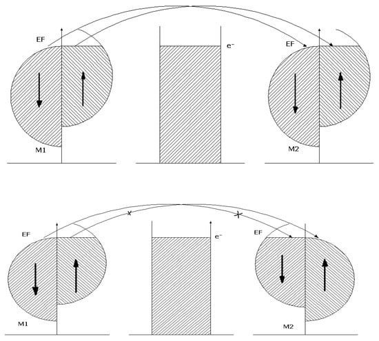
Figure 31.
Energy level density at magnet-insulator separating surface.
Consequently, one can write for respective currents [46]:
Here, Ia defines the electron current for the anti-parallel orientation of magnetic domains, while Ip defines the electron current for the parallel orientation.
D, as in the GMR case, signifies the energy level densities with indices (u,d), used to indicate the levels for “up” spin orientation and for “down” spin orientation, and indices (1,2) are used to indicate the first and second ferromagnetic layer, respectively.
In the literature, the following function (so-named ferromagnetic bias) is defined in order to characterize the density asymmetry near the Fermi level:
EF denotes the Fermi level again. For a nonmagnetic material where the densities are equal, this function is zero.
The effect of tunnel magneto-resistance (Equation (37)) can be transformed as follows:
ηtmr = (Rap − Rp)/Rp = (1/Rp − 1/Rap)/(1/Rap) = (V/Rp − V/Rap)/(V/Rap) = (Ip − Iap)/Iap = 2(Ip − Iap)/[Iap + Ip − (Ip − Iap)
Here V represents the applied voltage across the layer structure.
Using the above-given expressions for Ia and for Ib, the following usual expression for the TMR effect description is obtained:
If the ferromagnetic materials were strongly unbalanced, that is if Diu >> Did, then Pi ≈ 1 and η had a great value.
The anti-parallel spin orientation of the two ferromagnetic layers could be obtained by two methods:
- One of the ferromagnetic layers, say layer “1”, has a high coercive force (the magnetic field value which annihilates the magnetization [37]) or its thickness is high [56]. This is a hard magnet.
This could change the magnetic domain orientation only in the presence of a highly intense external magnetic field. Then, the second ferromagnetic layer, say “2”, separated from the first one by an insulator, must have a low coercive force (a soft magnet, such as perm alloy).
This constitutes a so-named spin-valve structure characterized by the fact that in the low intensity magnetic fields, only layer “2” changes its orientation while layer “1” maintains its orientation [57,58]. That means that the two layers will have a parallel or an anti-parallel mutual orientation of their magnetic domains depending on the external field orientation which is changed. Accordingly, the structure resistance will be changed from a high value (anti-parallel mutual orientation) to a low one (parallel mutual domain orientation) in function of the external magnetic field orientation. These structures can be realized both in GMR [59,60], and TMR cases.
The action of this structure is, for an electrical current, similar to the action of a usual valve on a gas flow.
- 2.
- One of the ferromagnetic layers is deposited over an anti-ferromagnetic layer and a strong mutual magnetic coupling appears between them, which gives the magnetic layer the property of a hard magnet with high coercive force [57].
Then the deposition of the structure is continued with the insulator and then with the soft ferromagnetic layer. This way the spin valve structure is obtained too.
Sometimes, the deposition process of the high coercive force ferromagnetic layer is made in the presence of an external magnetic field in order to improve the domain’s strong alignment.
Some of the obtained data using TVD will be presented further when experimental results are given [54].
Here, also as in the GMR case, the negative TMR effect can appear too, at least from the above-mentioned relation between the flip-flop spin relaxation distance and insulator thickness. If this distance could be smoothly changed by the applied fields within a decent variation domain of these, then one can change the electrical resistance of the structure no matter how the magnetic domain orientation in the two magnetic metals is.
The negative TMR structure was analyzed even from the very beginning of the GMR-TMR discovery [39].
7.3.2. Granular TMR
These depositions are made using two independently burning plasmas, one in the ferromagnetic atoms and the other in the evaporated molecules of the insulator. The main limitation comes from the insulator because TVD works with dc voltages. If the insulator material is heated indirectly in a conducting (usually tungsten made) crucible, it can generate a necessary atmosphere around the anode to ignite the plasma and to deposit the insulator simultaneously with the ferromagnetic material. Additionally, the insulating anode material can become a conductor at a high enough temperature.
Thereby, for certain insulators, such as SiO, MgO or MgF2, the authors of the present treatise proved that it was possible to ignite the plasma in their molecular vapors and to co-deposit them with magnetic material to build up a TMR granular structure [61], having the ferromagnetic atoms uniformly embedded into the insulator structure.
Therefore, it is possible to co-deposit Cobalt, or Nickel, or Iron with SiO, MgO or MgF2 and to obtain a TMR granular compound, by TVD technology. As an example, Figure 32 presents TMR curves for as deposited layers (black curves) and after a post-deposition thermal treatment.
Figure 32.
TMR curves for as-deposited Fe-Cu layers (black curves) and after a post-deposition thermal treatment (red curve).
To build up the optimal magnetic domain dimension in a just-deposited layer, it is usually necessary to subdue the deposited layers to a post-deposition thermal treatment in order to coagulate the magnetic atoms in optimal sized magnetic domains [62].
From Figure 32 and Figure 33, one can see the beneficial influence of post-deposition thermal treatment on the TMR effect. Namely, both the TMR absolute value and the steep side wings are substantially improved. This appearance can suggest that TVA deposition ensures a uniform atomic deposition (similar to thermal evaporation cases) and uniform domain coagulation. Indeed, in this case, all the magnetic domains are oriented for the same value of the applied external magnetic field, which is very useful for the devices that use such an active component.
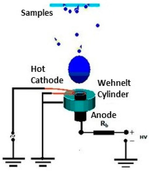
Figure 33.
The TVD tungsten deposition scheme and discharge image Reprinted with permission from Ref. [62]. © 2011, Romanian Academy Publishing House.
Here, as in a granular GMR case, the magnetic metal concentration must be optimal for an efficient TMR effect. The considerations made in the case of granular GMR and multi-layered TMR can be extended here.
7.4. Combined GMR-TMR, Ternary Depositions
As was above mentioned, the electrical resistance of the GMR structure compared with the TMR structure is very small. Sometimes it is necessary to have an intermediary resistance between these two.
In this case, one can try to obtain a combination between these two magnetic structures as to obtain a convenient resistance structure which can be of interest for special applications.
These special layers can be easily obtained by TVD technology [40], and this, at least, is due to the following considerations:
- -
- The evaporation sources in the TVD technology are punctual as in the thermal evaporation method;
- -
- The evaporations are processed in high vacuum conditions, and this gives the opportunity to ignite two or three separate discharges in an alternative or simultaneous mode, to obtain the desired composition of the deposited structure;
- -
- The depositions are obtained from plasmas generated in the genuine particles which are deposited to form the structure.
- -
- The added potentials applied on the substrates can contribute to improving the deposition characteristics by genuine ion bombardment;
- -
- By distributing the probe substrates on a given area above the three discharges, one can obtain suddenly (at once), a lot of material compositions on the probes due to their different geometry positions relative to the plasma sources. This gives the opportunity to perform a detailed analysis of the composition influence on the magneto-resistive effect, or in other cases on any other desired magnetic effect.
- -
- Additionally, it must be emphasized that there are no special conditions imposed to the forms or dimensions of the anode material to be evaporated.
- -
- Sometimes the depositions can be made without a crucible presence at the anode, as above mentioned.
The following structures can be obtained, proceeding as below:
- Deposit a simple, double or even triple ferromagnetic material or alloy;
- Deposit a nonmagnetic metal, alone or in combination with an insulator;
- Deposit a ferromagnetic combination over it:
- Repeat this structure as much as desired;
Another combination can be obtained as bellow:
- 5.
- Deposit a ferromagnetic layer;
- 6.
- Deposit a nonmagnetic conducting layer;
- 7.
- Deposit a ferromagnetic layer;
- 8.
- Deposit an insulator;
- 9.
- Deposit a ferro-magnet again;
Repeat the structure as much as desired.
Finally, a ternary mixture composed of ferro-magnet, nonmagnetic conducting metal and insulator forms a ternary granular mixture having different magneto-resistive effects.
Indeed, a lot of other possible combinations can be imagined and realized with TVD technology to study the material composition influence on the magneto-resistive effect.
All these last composites are nothing but a combination of GMR-TMR, multi-layered or granular structures deposited in order to obtain an optimum magneto-resistive effect, combined with a convenient electrical resistance of the structure.
The necessary conditions for a successful TVD application are:
- -
- A very good high vacuum (in the range of below 1 × 10⁻⁶ Torr);
- -
- An adequately sized deposition chamber;
- -
- Three high voltage electrical sources (some kV and some A);
- -
- Three low voltage sources for filament alimentation (some tens of volts, and some hundreds of A);
- -
- A high voltage (kV) low current source (microns), for probe biasing.
In the next section, dedicated to the experimental obtained structures in laboratory conditions, the different composite structures together with their TVD deposition characteristics will be presented.
They were carried out by the authors of this review article and are given as practical examples of deposition capabilities of TVD technology.
8. Single Conducting Material Deposition by TVD
As was mentioned above, it is possible to deposit a single material from an evaporating anode, or many component layers evaporated from different anodic sources. In this section, the different materials, as deposited by the TVD method, will be considered.
Both cases of different material deposition will be presented further: firstly single material depositions, and then different combined depositions, carried out by the TVD method.
8.1. Tungsten Deposition by TVD
Tungsten is the most known refractory metal having a melting point fixed at 3422 °C. This metal is recommended for high thermal resistance coverage of various tools, devices and installations.
However, because of the high melting point, tungsten cannot be evaporated from crucibles because there is no material to sustain the tungsten heated to a high enough temperature (above the melting point) to achieve a significant evaporation rate. The only possibility to produce a tungsten coating is by sputtering method, by arc, or TVD discharges. The TVD method appears to be the most advantageous, based on the following considerations:
- The TVD tungsten evaporation is proceeded especially through local electron bombardment of its surface.
Therefore, there is no need to increase all the tungsten body to very high temperatures.
- 2.
- The tungsten heat conductance is not very high (173 W·m−1 K−1) [56] and it allows to heat the tungsten anode surface up to a temperature situated just below its melting point (or even partially melted), maintaining at the same time the not bombarded surface of the anode in the solid self-sustaining state, when the evaporating temperature and deposition rates needed are not too high.
This way, the tungsten anode can be evaporated, with different evaporation rates from its proper “crucible”, as shown in Figure 33.
As seen from Figure 33, a tungsten rod is mounted on a thin tungsten wire which is fixed in the anode support. The use of this thin wire (of 1 mm diameter) can be possible because the discharge currents are small enough (of the order of an ampere) and can be easily evacuated through this wire. This way the heat loss is also minimized.
The obtained tungsten layer is characterized by a high purity (the cathode is also tungsten made) and well-structured network (the deposition is made in the presence of high energetic tungsten ion bombardment, and due to electron anode heating, the evaporated particles are highly made of tungsten atoms with no multi-atomic clusters).
The anode temperature, t, the corresponding vapor pressure, P, (Equation (10)) can determine the different evaporation rates, Vevap, from a square cm of anode surface, using Equation (12). With these data, the deposition rate, Vdep, at different distances from the anode can be calculated using Equation (14).
In the next figure, the deposition rates were plotted and calculated for a uniform deposition sphere [16], having a usual radius of 10 cm. This corresponds also for a deposition rate on a substrate situated at a 20 cm distance just above the anode and having tilt angles φ = θ = 0.
The melting point of the tungsten metal being 3422 °C, a tungsten anode upper surface heated up to a temperature as high as 3400 °C could ensure for the rest of the anode non-bombarded surface to remain solid during the deposition procedure.
Considering this temperature, from the given curves, one can obtain the deposition rate at 20 cm above the anode, of about 0.1 nm/s, as presented on the figure too.
Even this deposition rate might be at first glance too small, but for layers of 1 micron thickness with high purity and good structure, it becomes of interest. A higher deposition rate can be obtained when decreasing the anode-substrate distance and increasing the anode surface. Additionally, it is possible to cool the tungsten support in order to increase the anode upper surface to higher temperatures and, consequently, to obtain higher evaporation and deposition rates.
In fact, similar deposition rates as those evaluated above were measured using a quartz balance, when depositing tungsten by the TVD method [62] and using a scheme as the one presented in Figure 33. Figure 34 presents the typical evaporation rate, pressure and deposition rate dependence on the anode temperature at a distance of 20 cm from the tungsten plasma source to the measurement point.
Figure 34.
The evaporation rate, pressure and deposition rate at 20 cm from the tungsten plasma source.
In Figure 35, the V-I characteristics measured before and after the plasma generation in tungsten vapors when using the TVD deposition technology are shown.
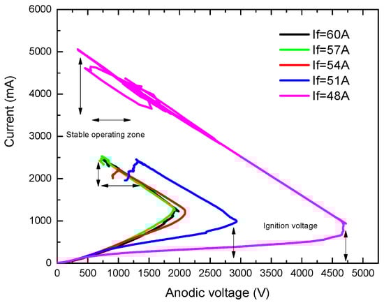
Figure 35.
V-I characteristics for TVD discharge when using a tungsten anode and different filament heating currents.
Their difference is determined by different cathode heating currents. As is readily seen, the cathode heating increase determines the decrease of the discharge breakdown voltage.
The cathode heating currents marked on the figure are: 48 A, 51 A, 54 A, 57 A and 60 A. When increasing the cathode heating current from 48 A to 60 A, the discharge igniting voltage decreases from 4570 V to 2000 V.
That is, for plasma ignition, it is not necessary to have a high value HV power supply capable of supplying 5000 V, but one with a maximum output voltage of 3000 V would be sufficient. The plasma emission color is blue (sky blue).
These curves were obtained through a steep increase in the applied voltage from the high voltage source until the discharge breakdown appeared, and then the voltage source Esour was maintained until the final working equilibrium point was attained. One can observe that the characteristics after the discharge breakdown are linear and approximately parallel with one another. The explanation of this behavior can be found when considering Equation (16) and taking the applied voltage from the source on the anode as constant after the plasma ignition.
In this case,
Vpl = E − RId → ∆Vpl/∆Id = −R= const.
Here, only Vpl and Id are variable, the value of the pure resistive load, R, remaining constant for the interval of current marked on the figure.
Therefore, the linear curves appearing after plasma ignition for all the filament heating currents have practically the same slope which in fact gives the loading resistance value (which was maintained constant) when no reactive components are present in the electrical circuitry.
When increasing the filament heating current, the electron thermo-emission from the cathode increases. As a result, more electrons are bombarding and heating the anode before plasma ignition.
Moreover, the number of pre-ignition electrons being greater for higher cathode heating, the discharge can be started even with lower vapor densities.
This allows the plasma ignition point to appear for lower anode potentials. The V-I characteristics are nearer when the filament heating current increases.
To increase the discharge current for lower applied voltages, one can decrease the load resistance value, Rload. This way, the inclination of the linear part of the discharge characteristics will increase and so will the power introduced into the plasma.
This power increase will increase the evaporation together with deposition rates.
The presented curves also suggest that if higher discharge powers are desired, it is necessary to decrease the filament heating current and increase the anode potential for an unchanged load resistance.
Another interesting phenomenon appearing during the tungsten deposition process by TVD technology is that after a long duration process, the filament is covered with a tungsten layer by the evaporated atoms coming from the anode.
This causes perturbation during the deposition process because the cathode heating is disturbed by increasing the filament diameter and, correspondingly, by decreasing the filament resistance.
This determines the filament heating current increase for a constant voltage applied on it. Finally, the thinner parts of the filament (with no tungsten vapor deposition on them) are superheated and broken and, consequently, the filament must be replaced. Generally, this replacement is necessary after the tungsten deposited layer thickness is around 1 μ and when using a filament made of a wire of 1 mm diameter.
If a thicker wire is used, say 2 mm, one can enlarge the deposition time, but it is necessary to have a source for filament heating able to furnish over a hundred A.
Tungsten depositions by TVD were intensely deposited and studied both as single materials and as a combination with others [63,64,65,66,67,68,69,70,71,72,73,74] for high temperature plasma facing walls in thermonuclear power plants (JET).
8.2. Carbon TVD Deposition
Carbon is the element with atomic number 14 and atomic weight 3.514 g/cm3. Its principal allotropic forms are graphite, diamond and amorphous [20].
While the diamond is transparent and has a low electrical conductivity, the graphite is black, opaque and is a good conductor. On the other hand, diamond possesses the greatest thermal conductivity and a very high chemical resistance.
At atmospheric pressure, it does not have a melting point, and its sublimation point is approximately 3900 K.
Diamond crystallizes in a cubic system and its hardness is one of the highest ones known.
Graphite is a good lubricant, crystallizes in hexagonal system and is a soft material.
The carbon work function is less than that of tungsten, namely 4.39 eV.
The amorphous carbon is completely isotropic and appears especially in thin layer deposited carbon.
The next plots present the vapor pressures, P, evaporation rates, Vev, and the deposition rates at 20 cm away from the anode, Vdep,20 (on the vertical starting from the anode surface), at different temperatures t, as in the above-presented tungsten case.
Comparing data from Figure 34 with the data from Figure 36, it is readily found that carbon evaporates easier than tungsten. Moreover, carbon has no melting point so that the carbon evaporation by the TVD method is easier than that for tungsten and requires no crucible to support the carbon material. In fact, the carbon arcs are burning between two carbon pieces with high currents and at high temperatures with no support crucible.
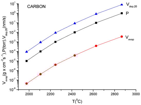
Figure 36.
The evaporation rate, pressure and deposition rate at 20 cm from the carbon plasma source.
Unfortunately, the carbon vapors interact with tungsten filament and can contaminate the carbon deposited material with traces of tungsten. Moreover, the melting point of tungsten carbide is 2870 °C and therefore is much under the boiling point of tungsten and this can induce a tungsten filament life shortening.
To avoid these undesired cases, and to obtain a high purity carbon deposition, one can use a carbon (instead of tungsten) filament as the thermo-electron emitter cathode.
This possibility is recommended by the lower carbon work function in comparison with the tungsten one, because this can allow for a better cathode electron emission (lower work function means higher thermo-emission, see Equation (3)). Additionally, the carbon sputtering is lower than that of tungsten, so there is no danger of carbon poisoning of the deposition, other than carbon.
The carbon deposited layers are found to be similar with the diamond structure so that they were given the name of diamond-like carbon or DLC. The DLC structures deposited by TVD are presented in [69,75,76,77,78,79,80,81].
These structures possess properties varying from those of graphite to those of diamond, depending on the ratio of sp2/sp3 inter-atomic bounding existent inside the deposited layer [75].
Shortly, the sp3 type bonding is formed by four valence electrons assigned to a tetrahedral directed network. This kind of orbital forms strong covalent bonds between the carbon adjacent atoms.
In sp2 type bonding, only three of four valence electrons are assigned to trigonal directed sp2 hybrid orbital and are forming strong covalent bonds with adjacent atoms on the same plane, while the inter-planar bounds are weak and ensures a soft characteristic of these kinds of links.
In sp1 type bonding, only two electrons form strong covalent bonds.
Depending on deposition method, two kinds of DLC layers can be obtained:
- a.
- Amorphous hydrogenated carbon coatings (a-C:H) which are deposited by plasma assisted chemical vapor deposition (PACVD);
- b.
- Tetrahedral amorphous carbon coatings (ta-C) or DLC hydrogen free coatings which are deposited by vacuum discharges, laser vacuum discharges, sputter depositions, etc.
As is obvious, the TVD technology allows for ta-C DLC layer deposition since it is carried out in high vacuum.
The DLC coating is frequently referred to as amorphous diamond, because its structure is locally tetrahedral, similar to diamond but is disordered on a larger scale. The ta-C coverage is stronger and with better friction qualities as compared with a-C:H ones [82].
One of the most important deposition parameters concerning the DLC film qualities is the energy of ions bombarding the just-forming deposit.
In TVD technology, the evaporated carbon atoms from the graphite anode are ionized by the electron-carbon atom collision, and as explained above, the neutral carbon atoms together with carbon ions are flying towards the over mounted substrates and deposit there.
Considering that the sp3 bonds are the strongest, the energetic ion bombardment of the just-forming layers encourages the sp3 bonding and removes the weaker sp2 bonds.
As a result, the TVD deposited DLC layers are expected to contain more sp3 bonds because the ion energies are of some hundreds of eV even when no bias is applied on substrates. Indeed, when the filament heating current is lowered, the discharge voltage must be higher for the same discharge current. The plasma potential which increases with anode potential, as presented above, is higher too. The plasma potential increase means that the plasma ion energy increases and a more intense bombardment of the earthen substrate will appear.
Moreover, even the carbon ion presence during the deposition can facilitate their acceleration towards the substrate.
Therefore, in TVD technology, besides the bias applied on the substrates, the carbon ion energy can be increased during the deposition by decreasing the filament heating current corroborated with anode potential increasing.
It is also important here to stress that the bombarding ions are of the same nature (that is carbon ions) as the material deposited, unlike in the sputtering case.
In thermal deposition methods, there are no ions present and there is no way to influence the deposition condition.
Moreover, the coating proceeds at a desired deposition rate, the condensate particles are atomic (they are generated from anode bombardment by electrons which, as above mentioned produces no clusters as ions when sputtering the cathode) and the structural arrangement is denser and with no conglomerates within the formed structure.
The deposition arrangement is similar to that presented for tungsten deposition, except the tungsten anode rod is replaced now by a graphite rod.
8.3. Rhenium TVD Deposition
Rhenium is a transition metal with the atomic number 75 and an atomic weight of 186.21 a.u. The melting point of rhenium is 3186 °C. Its crystal structure is hexagonal. In alloy with tungsten, it becomes a superconductor at 4–8 K. Rhenium density is 21.02 g·cm−3. Being a refractory metal, it is used to cover the gas turbines or other different pieces to protect their overheated parts against the excessive heating.
The vapor pressures, P, the evaporation rates, Vev, deposition rates at a 20 cm distance from the anode and Vdep,20 at different temperatures are given in Figure 37 above for rhenium.
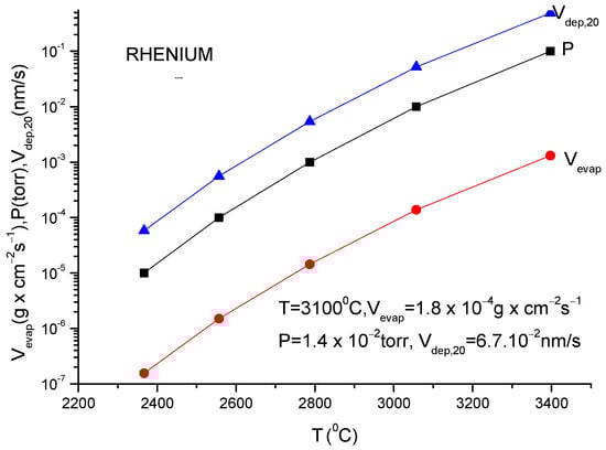
Figure 37.
The evaporation rate, pressure and deposition rate at 20 cm from the rhenium plasma source.
Comparing the data given here with those given for tungsten, it is found that the rhenium vapor pressures, and evaporating rates are greater than the tungsten ones.
Unlike carbon, the rhenium possesses a fixed melting point and what happens near this point is of interest, for example, at 3100 °C.
In Figure 37, the corresponding vapor pressure, evaporation rate and deposition rate at 20 cm away from the anode are shown. The deposition rate is around 0.67 nm/s which can be increased up to 1.2 nm/s when the distance of 20 cm is decreased to 15 cm. This deposition rate can be carried out without any crucible and is quite satisfactory for the deposition of layers having thicknesses of the order of a micron. Moreover, as stipulated for tungsten when higher evaporation rates are desired, the method cooling of the lower part of the tungsten rod can give the possibility for a higher temperature on the upper anode surface to be obtained with the beneficial consequences of decreasing the time of deposition.
The image (Figure 38) of rhenium TVD deposition with the electron gun arrangement is shown below:
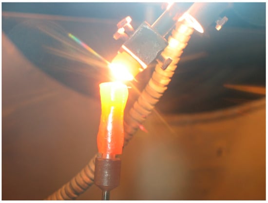
Figure 38.
Rhenium deposition from a rhenium anode rod.
The deposition rates measured during rhenium evaporation by TVD technology without any crucible and cooling proved to be of the same order of magnitude as this evaluated one.
As in the case of tungsten plasma, also here the plasma radiation is masked by the intense anode thermal radiation.
It is worthwhile to describe here an interesting phenomenon appearing during rhenium deposition process by TVD.
The tungsten filament work function (electron extracting energy) is 4.5 eV or even less when allied with thorium. On the other hand, the rhenium work function is 5.1 eV.
That means that when rhenium atoms evaporate from the anode and come towards the filament, they can cover the filament surface and remain there for a long time, being also a refractory metal with a high desorption energy, H [83].
This can determine the filament work function increase, as the Formula (8) indicates. This equation shows that the higher the anode temperature, the greater the filament rhenium coverage and the higher the filament work function. However, from Equation (3), this phenomenon leads to a lower electron thermo-emitted current and finally a discharge current decease is observed.
Moreover, an anode potential increase increases rhenium evaporation and rhenium cathode coverage and decreases the discharge current by decreasing the cathode electron emission.
As a conclusion, after the discharge breakdown, the discharge current decreases when increasing the anode potential.
To increase the discharge current and anode evaporation, one has to increase the cathode heating current which can restore the filament work function and the filament emitted current, as seen from the Equation (8). Rhenium depositions by TVD method are presented in [84].
8.4. Beryllium Deposition by TVD
The atomic number of this alkali metal is 4, and its atomic weight is 9.012183. The melting point of beryllium is 1287 °C and the boiling point is −2469 °C. The crystalline structure is hexagonal and from the magnetic behavior point of view, beryllium is a diamagnetic metal. The beryllium density is 1.847 g/cm3.
The vapor pressures, P(torr), the evaporation rates, Vev (g·cm−1·s−1), and the deposition rates at 20 cm distance from the anode, Vdep,20, are given in the next figure, as a function of the temperatures in °C.
As beryllium has a certain melting point, it is worthwhile to see just under this point to appreciate if it is possible to evaporate this material without any crucible as the materials presented before.
As the beryllium melting point is 1287 °C, it would be interesting to see the evaporation rate for t = 1250 °C.
As shown in the Figure 39, the deposition rate at 20 cm distance from the beryllium anode is 0.35 nm/s which can be increased for smaller distances and larger anode heated surfaces.
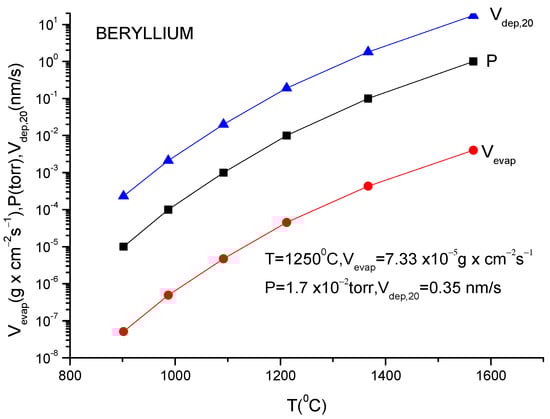
Figure 39.
The evaporation rate, pressure and deposition rate at 20 cm from the beryllium plasma source.
This is a quite satisfactory deposition rate for most of the interesting beryllium deposition cases and can be carried out from a beryllium rod having one square cm surface area, without any crucible. Therefore, no crucible material is expected to be found in the beryllium coverage, with the TVD technology when layer purity is of major importance. When cooling the lower part of beryllium rod, the higher deposition rates were obtained by the authors of this review article.
In Figure 40, TVD blue plasma, ignited in the beryllium vapors, is shown.
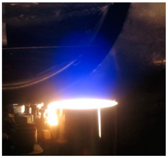
Figure 40.
Pure beryllium, TVD plasma.
The usual blue plasma is formed in beryllium vapors while depositing beryllium coverage by TVD technology.
A particular behavior of the beryllium deposition process is the possibility of a surface beryllium oxide formation when the base pressure during the deposition is not sufficiently low.
As the beryllium oxide melting point is much higher than that of beryllium one (2507 °C), and as it is a compact layer, the following problem can appear. The surface bombarded by the electron flux evaporates the pure beryllium more rapidly than the surrounding oxide layer, and caves could be formed in the beryllium rod, in this way impeding the beryllium deposition. Works dedicated to beryllium TVD depositions can be found in [82,85,86,87,88,89,90,91,92,93,94,95,96,97,98,99,100,101].
8.5. Boron Deposition by TVD
Boron is the following element in the periodic table having the atomic number 5, and atomic weight 10.811. The boron density is 2.46 g·cm−3. It is a metalloid, and it is not expected to be appropriate for TVD deposition technology treatment. Nevertheless, the boron TVD depositions were already carried out for thermonuclear coverage of first wall tiles and for X-ray transparent windows. The explanation may be the fact that this element is non-conducting at room temperature, but its conductibility increases with the temperature at a level which permits the boron anode of TVD to remove the discharge current. The small boron pieces are melted and sustained by a glassy carbon crucible, as shown in Figure 41 [102].
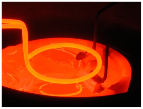
Figure 41.
Boron melted anode in a glassy carbon crucible.
The boron plasma cannot be visually seen from the thermal anode intense radiation, as happens with other refractory materials evaporated by TVD. However, the existence of plasma was detected by V-I characteristics.
In the next figure (Figure 42), as in the preceding ones, the vapor pressure, P, the evaporation (Vevap) together with deposition rates (on a probe mounted at 20 cm distance from the anode) Vdep,20, at different temperatures, are given for boron.
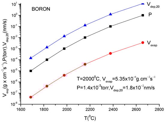
Figure 42.
The evaporation rate, pressure and deposition rate at 20 cm from the boron plasma source.
As shown in Figure 42, for an anode surface temperature of 2000 °C the evaporation rate from a square centimeter is Vevap = 5.35 × 10⁻⁶ g·cm−2·s−1. The corresponding deposition rate at a 20-cm distance from the anode for θ =φ = 0 is 0.18 Ä/s, which in many cases can be satisfactory for high quality deposition made without a crucible.
However, with this low deposition rate, one would need 18 days of continuous deposition by TVD at a temperature situated under the boron melting point (when not, crucible use is not necessary) to obtain a layer thickness of 50 μm.
Instead, when using a glassy carbon crucible, the boron granules can be heated for example up to a 2377 °C temperature when boron is melted while the carbon remains solid because its melting point is 3547 °C.
At this temperature, the obtained deposition rate becomes 1.2 nm/s. At this rate, 50 microns would be coated in about 11 h. In fact, the real deposition time for a 50 μ thick boron layer was about 24 h because the deposition geometry was not the same as that used for calculation.
However, in this case, some carbon atoms are evaporated too, and the layer purity is affected by carbon.
8.6. Copper Layer TVD Deposition
Copper is one of the most adequate conducting metals to be deposited by the TVD method. Its atomic number is 29, the atomic weight is 63.546 a.u., the melting point is 1083 °C and the boiling point is 2595 °C. The copper density is 8.94 g/cm3. The copper vapor pressure, copper evaporation rate and copper deposition rate at 20 cm distance from the anode as a function of temperature is given below in Figure 43.
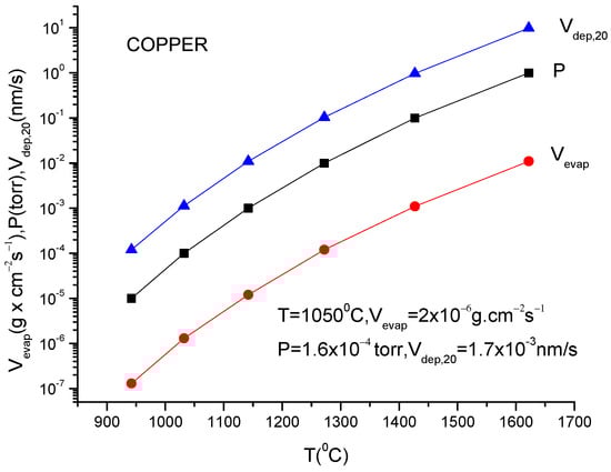
Figure 43.
The evaporation rate, pressure and deposition rate at 20 cm from the copper plasma source.
To evaluate the possibility to deposit copper without a crucible, the anode surface temperature 1050 °C can be used.
The corresponding evaporation rate from a square cm of anode surface is 2 × 10⁻⁶ g·s−1. The copper deposition rate at 20 cm from anode is very small, namely 0.017 Ǻ/s. In this case, if a copper layer of 10 nm thickness is desired (this is the usual thickness used for GMR structures) the deposition time would arise to 2 h and 6 min. The deposition time is not extremely long but, as explained above for the GMR structures, it is necessary to deposit many copper layers which makes the TVD method uncompetitive.
In Figure 44, two evaporation arrangements are presented for the copper vapor green plasmas.
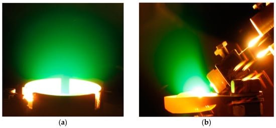
Figure 44.
Copper TVD plasmas. (a) Ring cathode structure; (b) electron gun structure.
Habitually, the crucible materials used for copper evaporation are alumina, molybdenum or tantalum, the last two being of interest in TVD technology. The melting point of molybdenum is 2617 °C while that of tantalum is 2996.
Small chunks of copper can be heated in these crucibles up to a temperature of, ~1600 °C without any problem. At this temperature, the copper deposition rates of 111.73 nm/s can be obtained which is quite satisfactory.
In Figure 45, different curves of V-I characteristics obtained in the copper vapors for different filament heating current are written on the figure.
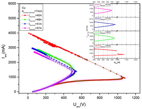
Figure 45.
V-I characteristics for TVD copper plasma burning for different filament heating currents.
A lot of studies were carried out in copper, silver, aluminum, etc., TVD plasmas [81,87] among them being the ones given above for copper deposition as determined by different plasma parameters.
These V-I curves are similar with those given for tungsten and the explanation presented there is also valid here.
The filament heating current decrease is similar to the anode-cathode distance increase, as was found out experimentally.
As an example, Figure 46 shows characteristics drawn for anode-cathode distances of 7 mm,10 mm, 13 mm and 14.5 mm and for a filament heating current of 48 A when the discharges were carried out in copper vapors. Similar curves were obtained in other metal vapors.
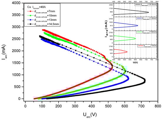
Figure 46.
Copper plasma V-I characteristics for different inter-electrode gaps.
Among the many other works published on TVA copper depositions, the following ones can be mentioned [29,103].
8.7. Silver Layer Deposition by TVD
Silver is another transition metal having the atomic number 47, the atomic weight 107.8642 a.u. and the density 10.49 g·cm−3. The melting temperature of silver is 961.78 and the boiling point is 2162.
Again, the graph, with the vapor pressure, evaporation rates from the unit silver anode surface and silver deposition rate at 20 cm, are presented below (Figure 47) as depending on anode material temperature.
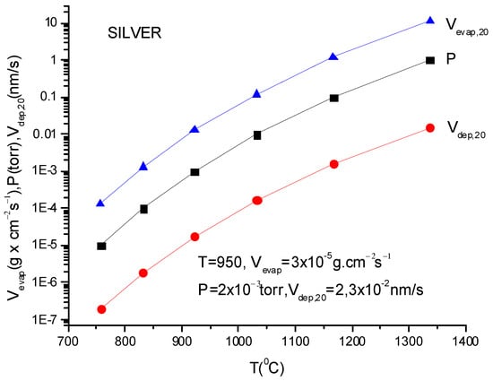
Figure 47.
The evaporation rate, pressure and deposition rate at 20 cm from the silver plasma source.
The melting point of silver being 961.78 °C, an evaporation temperature of 950 °C can be taken into account for further evaluations.
At this temperature, the evaporation rate is 3 × 10⁻⁵ g·cm−2·s−1, and the uniform deposition rate on a sphere having a radius of 10 cm is 2.3 × 10⁻² nm/s, which is small enough but not too small to not be considered when high quality layers are desired.
Indeed, the small heating temperatures can be maintained when a low heating current for the filament and low anode potential are used. In fact, the anode heating can be made only by thermo-emitted electrons (before plasma ignition).
Fortunately, tungsten, molybdenum and tantalum baskets or crucibles can be used for silver TVD deposition. The image of TVD silver plasma is given in the Figure 48.
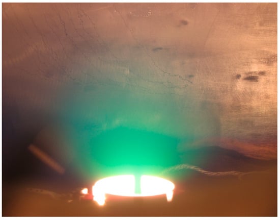
Figure 48.
The silver TVD plasma image with ring cathode arrangement.
Then, the corresponding deposition rates would increase to 450 nm/s or even more.
Figure 49 displays the V-I characteristics for a discharge burning in the silver vapors for different anode-cathode distances. Comparing these curves with those given for a discharge burning in the copper vapors at a fixed anode-cathode distance, but for different cathode heating currents, their similitude is obvious. Indeed, the cathode-anode distance increase (when electron focusing action of Whenelt is worse) is similar to the thermionic emission current decrease due to electron spread out, having as a result the electrons surface density decrease at the anode.
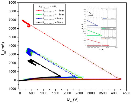
Figure 49.
V-I characteristic for silver vapor discharge for different anode-cathode distance (marked on the figure) and the same cathode heating current (45 A).
Here, it also appears that the discharge parameters arrangement is after the first impulse burst just after the discharge break-down and this indicates that the stable working point of the plasma corresponds to lower discharge currents and higher anode voltages.
In fact, just after the breakdown, the ionizing rate increases rapidly and so does the discharge current. However, during the discharge time, the energy introduced by the electrons into the anode changes in comparison with that introduced at the knee point of the characteristics.
The number of electrons coming from the discharge now is by far greater than that at the breakdown point and the anode voltage is lower. This changes the anode evaporation rates and ionization rate of the vapors which can be lower than at the knee point of the characteristics.
This would determine a slow discharge current decrease after the instantaneous final point on the characteristics is reached.
This is accompanied by a discharge voltage increase when the source potential, E, is not changed. As a result, the instantaneously obtained discharge point slowly changes its position on the V-I characteristics towards the lower current-higher voltage equilibrium point.
Note that the equilibrium final is reached after the new vapor density is stabilized by thermal effects.
When judging those phenomena, one must consider the heating process as taking place at the same time with electric processes and in direct interdependence with each other. However, the thermal phenomena usually develop slower in comparison with the electric ones.
8.8. Aluminum Deposition by TVD
Aluminum is the element with atomic number 13, atomic weight 26.892 a.u. and bulk density 2.7 g·cm−3. Its melting point is only 660 °C, but the boiling point is 2519 °C.
Figure 50 highlights the thermal evolution of the vapor pressure, evaporation and deposition rates for aluminum anode, as in previous cases.
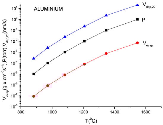
Figure 50.
The evaporation rate, pressure and deposition rate at 20 cm from the aluminum plasma source.
The deposition rate of aluminum for the lowest given temperature, that is 882 °C, is obtained as above to be 2.6 × 10⁻⁴ nm/s at 20 cm from the anode. This deposition rate is indeed too low for layer deposition of usual thicknesses. In this case, if someone would try to deposit aluminum at a temperature situated under the melting point (660 °C) to avoid the crucible use, they would have to wait a very long time to obtain an aluminum layer of a micron thickness for example.
The frequently used refractory metals (W/Ta/Mo) cannot be used since aluminum alloys with them and drastically decrease their melting point [104].
Fortunately, the aluminum can be coated from BN, or TiB2-BN, or ZiB2 crucibles [96]. In this case, if one increases the anode temperature up to 1547 °C, the deposition rate of around 2.9 × 10³ nm/s is reached, which is quite satisfactory even for industrial coverage when aluminum is intended to be used, for example, for its high reflection index, in mirror production.
In Figure 51, an aluminum TVD plasma is shown.
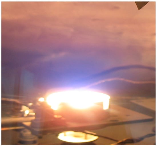
Figure 51.
The aluminum TVD plasma image.
Here, the anodic vacuum arc technology for industrial aluminum deposition on polymers must be revealed [105].
8.9. Nickel Layer Deposition by TVD Technology [106]
Nickel’s atomic number is 28, atomic weight is 58.6934 a.u. and density is 8.9 g·cm−3. The nickel melting point is 1455 °C and its boiling point is 2913 °C.
Nickel is a transition ferromagnetic metal, and it is largely used in layers in GMR-TMR technologies and in other scientific and industrial domains.
The nickel vapor pressures and evaporation-deposition (at 20 cm) rates are presented in Figure 52 and are given for different temperatures:
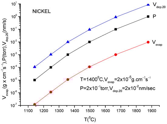
Figure 52.
The evaporation rate, pressure and deposition rate at 20 cm from the nickel plasma source.
In the following, the nickel deposition rate at 20 cm will be evaluated when a nickel rod is heated up to near melting point, say 1400 °C.
The deposition rate as high as 0.2 Ǻ/s. at 20 cm from the anode can be obtained, as shown on Figure 52.
This deposition rate may be sufficient for layer deposition in GMR-TMR structures where usual thicknesses are of the order of nanometers and high purity depositions are desired. Additionally, this deposition rate can be increased by the reduction of the anode-substrate distance or by increasing the anode heated surface simultaneously with an adequate cooling of the lower part of anodic nickel rod.
This ensures the magnetic layer’s high purity, which is crucial in GMR-TMR structures.
Higher deposition rates are achieved when laying nickel chips in alumina, beryllium oxide or glassy carbon crucibles. The last crucible in these examples is the handiest since it is a sufficient conductor from an electrical standpoint. The nickel TVD plasma image is given in Figure 53.
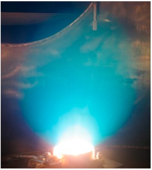
Figure 53.
The nickel TVD plasma image, generated with ring cathode geometry.
8.10. Iron Deposition by TVD Technology
Iron is another transition ferromagnetic metal (Curie point 770 °C) with the atomic number 26, atomic weight 55.845 a.u., density 7.874 g·cm−3, melting point 1538 °C and boiling point 2868 °C.
The vapor pressures p, rate of evaporation Vev and rate of deposition Vdep,20 at 20 cm are given as usual in Figure 54 below.
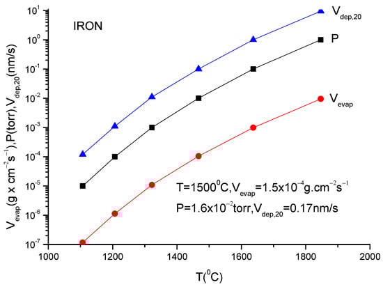
Figure 54.
The evaporation rate, pressure and deposition rate at 20 cm from the iron plasma source.
The evaporation temperature below the melting point can be chosen as 1500 °C. From the above plot, the evaporation rate is 1.5 × 10⁻⁴ g/(cm2·s) and the corresponding deposition rate at 20 cm from the anode would be situated around 0.17 nm/s, a value which is sufficiently high to ensure layers deposition in GMR-TMR structures without any crucible in the benefit of deposition purity.
For higher deposition rates with lower layer qualities, one can use alumina or glassy carbon made crucibles. When using alumina crucible, a special experimental arrangement must be made to ensure the discharge current evacuation through the anode.
For example, when the anode temperature is 1847 °C, the deposition rate could attain 75 nm/s.
An iron TVD plasma image is similar to that given for nickel TVD plasma.
8.11. Cobalt Depositions by TVD
Figure 55 presents the typical evaporation rate, pressure and deposition rate dependence on the anode temperature at a distance of 20 cm from the cobalt plasma source to the measurement point.
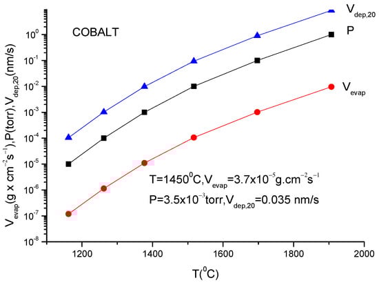
Figure 55.
The evaporation rate, pressure and deposition rate at 20 cm from the cobalt plasma source.
Cobalt is also a transition ferromagnetic metal with the atomic number 27 and atomic weight—58.933 a.u. The cobalt bulk density is 8.9 g/cm3.
The melting point of cobalt is 1495 °C and boiling point is 2927 °C, while the Curie point is 1115 °C. The following graph gives the corresponding thermal values for cobalt.
The deposition rate at 20 cm from the anode at a temperature of 1450 °C is around 0.35 Ǻ/s, which might be good enough for GMR-TMR depositions. Additionally, the cooling technique of the lower part of the cobalt rod in order to increase the upper anode surface temperature can be applied in order to avoid the crucible use and to obtain a layer with increased purity.
For higher deposition rates, the alumina and beryllium oxide crucibles can be used with an appropriate electrical montage to evacuate the charges from the plasma.
When heating the anode up to 1907 °C, the deposition rate increases to 8.6 nm/s.
Cobalt TVD plasma is similar to those of nickel and iron.
The GMR-TMR layers containing cobalt as a ferromagnetic component are particularly performant [67]. The usual crucible materials are the same as those for the previously given ferromagnetic metals.
8.12. Chromium Deposition by TVD
Chromium is a transition metal with atomic number 24, atomic weight 51.996 and bulk density 7.19 g·cm−3. Its melting point is 1907 °C, and at the temperature of 38 °C, it transforms from an anti-ferromagnetic metal to a paramagnetic metal.
This metal was combined with iron to create the first GMR structure which demonstrated a GMR effect at low temperature [70].
The next graph gives the thermal parameters of the chromium anode (Figure 56).
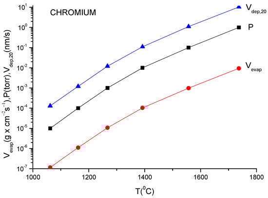
Figure 56.
The evaporation rate, pressure and deposition rate at 20 cm from the chromium plasma source.
As one can see, the chromium metal has a high melting point in comparison with the other transition metals so far presented here. Therefore, the deposition rate at 20 cm away from the anode can be obtained just as an evaluation, taking the last presented temperature, namely 1737 °C, which is safely situated under the melting point of chromium.
The deposition rate is found out to be around 103 nm/s, which is quite satisfactory for most chromium coverage.
Because chromium metal is coming as individual fragments, it is evaporated from a glassy carbon crucible. Tungsten crucibles can also be used for chromium evaporation in TVD technology.
A chromium TVD plasma image is given in Figure 57.
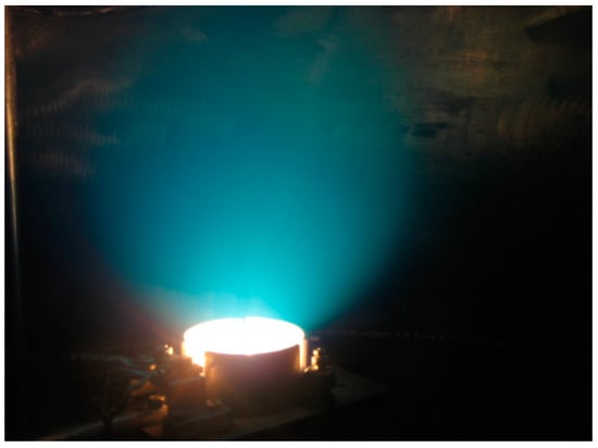
Figure 57.
Chromium TVD plasma image generated in the ring cathode geometry.
8.13. Iridium Deposition by TVD Method
Iridium is a transition metal with an atomic number of 77 and an atomic weight of 192.217. The density of its solid state is high, namely 22.56 g/cm3, and its melting point, 2466 °C, together with the boiling point, 4428 °C, are also high.
For this reason, iridium can be used as a high temperature resistant (refractory) material.
From the TVD deposition point of view, the Figure 58 will present the thermal data for iridium.
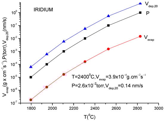
Figure 58.
The evaporation rate, pressure and deposition rate at 20 cm from the iridium plasma source.
A quick examination of the presented data for iridium permits to evaluate that a high deposition rate is very difficult to be attained with this metal. Furthermore, the only crucible that may be utilized in this instance is one composed of thorium dioxide.
However, for low deposition rates, let one see what happens under the melting point of iridium (2400 °C) when no crucible is necessary.
An approximate evaporation rate from the iridium anode surface of 1 cm2, when heated at this temperature, is 3.9 × 10⁻⁴ g/(cm2s).
Then the evaluated deposition rate at 20 cm away from the anode might be 0.14 nm/s, which is convenient for the deposition of GMR-TMR layers of some nanometers thickness. For higher deposition rates, the cooling of the lower side of the anode can be used but it would have a detrimental influence concerning the energy consumption (time spare = energy waste and conversely).
This metal can be used in combination with manganese, in spin valve fabrication, for anti-ferromagnetic type layer deposition.
The iridium plasma radiation is again masked by a high intense anode thermal radiation, as it can be seen in Figure 59.
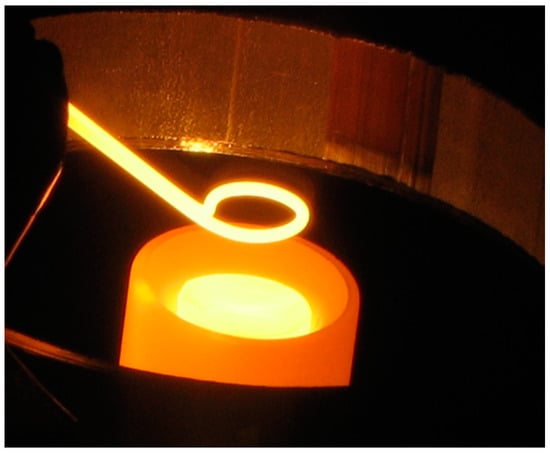
Figure 59.
Iridium plasma from a melted anode.
The presence of plasma is once more sensed by the V–I characteristics of the discharge.
8.14. Manganese Deposition by TVD Technology
Manganese is also a transition paramagnetic metal, having the atomic number 25, atomic weight 54.938 a.u., bulk density 7.21 g/cm3, melting point 1246 °C and boiling point 2061 °C.
The manganese thermal behavior is presented below with the same parameters as before (Figure 60).
Figure 60.
The evaporation rate, pressure and deposition rate at 20 cm from the manganese plasma source.
Under the melting point value, the expected deposition rate for this metal is around 9 nm/s, as shown on the Figure 61, which is a high enough deposition rate for usual layer thicknesses of interest for magneto-resistance structure production. This makes it possible to produce manganese coverage, even without any boat or crucible support, and this can contribute to also obtain a purer layer.
Figure 61.
The evaporation rate, pressure and deposition rate at 20 cm from the magnesium plasma source.
In case a higher deposition rate is necessary, tungsten, tantalum or molybdenum crucibles can be used.
8.15. Magnesium Deposition by TVD Method
Magnesium is an alkaline earth metal with atomic number 12, atomic weight 24.05, bulk density 1.738 g/cm3, melting point 650 °C and boiling point 1091 °C.
The next figure is dedicated to temperature dependence of the usual parameters for magnesium.
The magnesium deposition rate at 20 cm away from the anode was evaluated to 32 nm/s at an anode temperature of only 600 °C.
To summarize, if the magnesium anode of 1 cm2 is heated at a temperature of 600 °C, which is under the magnesium melting point, so that the rest of un-bombarded anode surface remains solid, a sufficient deposition rate can be obtained on a surface mounted 20 cm away from the anode.
For higher deposition rates, one can use boat-type crucibles made of tungsten, molybdenum, tantalum and glassy carbon as boats, or crucibles. Above the melting point, high deposition rates could be attained with TVD technology.
9. Non-Conducting Material Deposition by TVD Method
9.1. Silicon Deposition by TVD Method
Silicon is a semiconductor having the atomic number, 14, the atomic weight, 28.086 a.u., and the density of the solid state, 2.32 g·cm−3. Silicon melts at a temperature of 1414 °C and boils at 3265 °C.
The temperature dependencies of silicon parameters are presented in the following graph.
As seen from Figure 62, at 1400 °C, which is just under the silicon melting point, the deposition rate is 0.02 nm/s, which is very low if thicknesses in the range of one micron are needed.
Figure 62.
The evaporation rate, pressure and deposition rate at 20 cm from the silicon plasma source.
Fortunately, one can use a boat-type crucible made of tungsten or tantalum, or crucibles made of beryllium oxide, tantalum or glassy carbon. In all these cases the anode temperatures can be safely raised up to a temperature of 1717 °C where the evaporation rate might be 6.93 × 10⁻⁴ g/(cm2·s) and the corresponding deposition rate at 20 cm away from anode becomes 2.4 nm/s, which becomes satisfactory. If the silicon anode temperature is raised up to 1927 °C, which allows for an evaporation rate of 6.59 g/(cm2·s), the deposition rate becomes 23 nm/s, which permits for example to deposit a layer of 1 micron thickness during a time lapse of 44 s [107,108].
Silicon is one of the most used elements in thin layer depositions for a lot of many known industrial and scientific application.
The fact that silicon resistance decreases with temperature, allowing for more free charges generation in the conduction band and thus allowing for resistance decrease, ensures that TVD can be used for silicon deposition.
9.2. Magnesium Oxide Deposition by TVD
This substance is usually in the form of a white powder, with a density of 3.58 g/cm3, a melting point of 2852 °C and a boiling point 3600 °C.
It is a very good insulator (electrical) and a refractory material too. It can be used for magneto-resistance structures deposition, or for crucible preparation. It also can be used as a protective layer in plasma displays manufacture when it also contributes to a better secondary electron emission from the ion hit cathodes.
This material creates a vapor pressure of 10−4 Torr at 1403 K, 10−2 torr at 1683 K and 1 torr at 2073 K. Considering the last temperature, which is well under the melting point of magnesium oxide, one can evaluate the deposition rate on a probe situated at 20 cm from the MgO anode.
This deposition rate can attain a value of about 18 nm/s, which is high enough and can be increased if the anode temperature is raised up to say a 2700 K temperature.
That means that magnesium oxide can be efficiently deposited without a crucible and the deposition rates can be more than adequate for TMR deposition structures.
Even if magnesium oxide is a good electrical insulator, it was still coated using the TVD technology.
It was probably possible since the higher temperatures increase the magnesium oxide conductance, allowing the dc current to flow through the anode, though the discharge current is not as high as in the arc discharges technologies.
9.3. Magnesium Fluoride TVD Deposition
Another insulating material which was deposited by the TVD deposition method is magnesium fluoride. This substance has a molar mass of 62.3 g/mol, a density of 3.148 g/cm3 and a melting point of 1263 °C (vis. 1536 K). This material is intensely used in optics as anti-reflex coatings and in TMR deposition too. Its coatings are transparent over an extremely large wavelengths domain of electromagnetic radiation.
The vapor pressures of MgF2 are 10−4 torr for temperature 1175 K, 10−2 torr for 1390 K and 1 torr for 1710 K.
The corresponding deposition rates at 20 cm from the TVD anode whose cross section is 1 cm2 are: 0.034 Ä/s, 0.31 nm/s and 28 nm/s, respectively. Under the melting point of this material, the deposition rates are of the order of Ä/s, which can be satisfactory for TMR structures whose thicknesses are of the order of a nanometer.
But higher deposition rates can be obtained when using crucibles made of molybdenum or tantalum.
Another material which was successfully deposited by the TVD method is silicon oxide and other insulating materials can be deposited by this method.
At the end it must be added that the aluminum oxide deposition by the TVD method was not successful because a strong decomposition of the oxide appeared during the deposition process.
But for the TMR structures, deposition one can use aluminum deposition together with an alternate anodization of the aluminum layer in oxygen discharges.
At the end of this section, it must be underlined that all the calculated deposition rates are valid only for the cases of thermal evaporation when the evaporated particles are neutral and uniformly distributed in space.
In the case of TVD technology, parts of the evaporated particles are transformed into ions which are under the influence of electric potential distribution.
In this circumstance, most of ions are attracted towards the cathode and do not contribute to deposition, especially in case of the electron gun structure when the cathode (which attracts the ions) is mounted aside from the anode-substrate line. Therefore, the above obtained deposition rates must be diminished with the contribution of the number of the ion evacuated to the cathode. If the discharge current is not too high, this influence is negligible but for the higher currents and especially in the electron gun arrangement (as above shown), the following expression must be subtracted from the deposition rates presented above: (Id/e) (M/NA)/ρ (cm/s).
Being aware of all these, one must try to produce the deposition at a relatively low discharge current value to obtain a high deposition rate, good adhesion and high density layers. This can be accomplished by changing both the cathode heating current and/or the load resistance.
10. Practical Simultaneous TVD Depositions
In Figure 63, an arrangement for different binary deposition is shown.
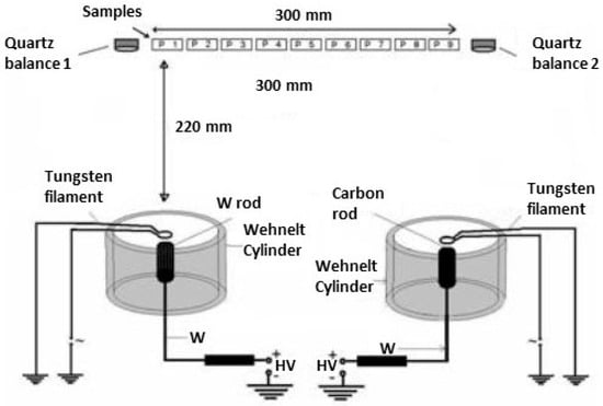
Figure 63.
Example of TVD tungsten, carbon codeposition arrangement.
The deposition is carried out from two independent discharges. The right discharge is initiated from a typical anode montage used in the case of carbon, tungsten, rhenium, or any other high temperature melting substance able to create a sufficient vapor pressure for a special deposition case to obtain a sufficient deposition rate, as above described.
In these cases, the rod type anodes are consumed by evaporation as a candle when burning.
Figure 64 represents the deposition scheme from an anode with crucible in order to sustain the melted material. Over the anodes, the tungsten-made ring cathodes are shown, while around the anode and cathode the Whenelt cylinders are mounted, which ensure the electrical separation of the discharges and thermo-electron focus.
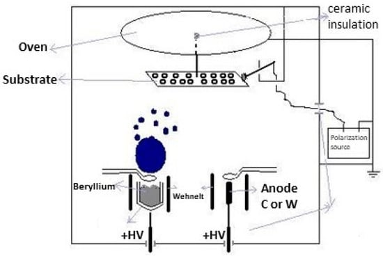
Figure 64.
Example of binary beryllium, carbon or tungsten TVD co-deposition arrangement.
Different biases were applied to the rotatable substrate to study the effect of genuine ion bombardment on the coverage structure.
Additionally, a fixed oven mounted in the rear side of the substrate permits to study the substrate heating on the layer structure and in Figure 64, comparable SEM data are presented which justify the beneficial influence of the negative bias.
With this scheme, carbon or tungsten mixed with beryllium or single element depositions were produced [70]. As an additional remark, this technique was used for the marker coatings consisting in mixed beryllium and nickel layers for a selection of bulk beryllium tiles in the main chamber, and a tungsten coating of the carbon fiber composites (CFC) in the divertor region of the Joint European Torus (JET) tokamak at Culham, in the ITER-like wall (ILW) era [109,110,111]. A graphical representation of the inside of the JET fusion nuclear plan is given bellow on the Figure 65.
Figure 65.
The inner side of the ITER tokamak. Left side shows early vessel inspection before ILW era. Right side, thermonuclear discharge at work.
The left-side part shows the inner part early stage of the JET reactor, before the ILW project which consisted of Be tile in the main chamber, and bulk W and W-CFC in the divertor area, while the right image shows the luminous ignited thermonuclear plasma.
The above presented coverage was useful for material erosion and redeposition studies performed in JET.
This kind of coverage can also be useful for the high energy (heat) protection of the different components of the thermal motors, also [72].
In Figure 66, a comparison is made between a layer deposited by a TVD technology (left figure) and a layer deposited by thermal evaporation (right figure) when no ions are present.
Figure 66.
SEM images for a TVD deposited layer (left) and a thermal deposited layer of the same material (beryllium) (right).
With a similar scheme presented in the Figure 63 and Figure 64, different combinations of refractive materials such as Re + Ni, W + C + Be, etc. were deposited by the TVD method, especially with a ring cathode arrangement [88].
When a uniform concentration distribution throughout the film is desired, the substrate is continuously rotated during the deposition.
However, when a large variation in concentration on different substrates is desired to study the characteristic of composite deposition as determined by different component concentrations, the facility of material evaporation occurring from separate punctual sources (anodes) in TVD technology can be used. Indeed, by mounting a substrate holder above and between the evaporating sources and attaching different separate substrates to it, one can obtain a wide range of compositional probes in a single act of deposition depending on the relative position of the substrates relative to the evaporation sources.
In the case of granular magneto-resistive deposition, it is often necessary to use different crucibles which do not interact with the material intended to be evaporated, as presented when different materials were discussed.
In general, crucibles made of glassy carbon or alumina are of interest for these applications. In the case of alumina, there appears to be an issue with its electrical conductance, but a solution can be found even in these cases to ensure the electron withdrawal from the anode.
One such possibility is to sustain the alumina crucible on a support made of the same material as that to be evaporated and to allow the electric contact by practicing a small orifice at the bottom of the crucible though which a metallic wire will conduct the anodic currents.
The benefit of TVD technology is that the discharge currents are small, and the voltages are high, which does not require very good electrical contacts as in arc discharge cases. In Figure 67, a practical arrangement is given which permits the deposition of nine different materials in layers as is the case of multilayered GMR-TMR depositions and the simultaneous deposition of two materials for granular structures, as used in [96].
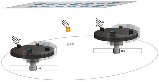
Figure 67.
Electron gun TVD deposition for mixed ternary composite layer or for 9-multilayer deposition with different materials.
Two carbon rotatable discs sustain four different crucibles each, and the third one ensures, when desired, a ternary layer deposition from three simultaneously burning sources. Deposition arrangement is that with three electron gun cathodes schematically shown on the figure.
Some magneto-resistive multi-layers obtained by this method are schematically presented below.
Figure 68 describes a ternary composite GMR-TMR layer in a granular of structure made of cobalt as a magnetic metal, copper as a conducting metal and magnesium oxide as an insulator, having tantalum as the bottom and top layer, all being deposited on silicon substrate.
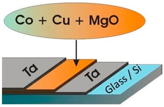
Figure 68.
Example of GMR-TMR granular deposits by TVD technology.
Another structure is presented in Figure 69 [40].
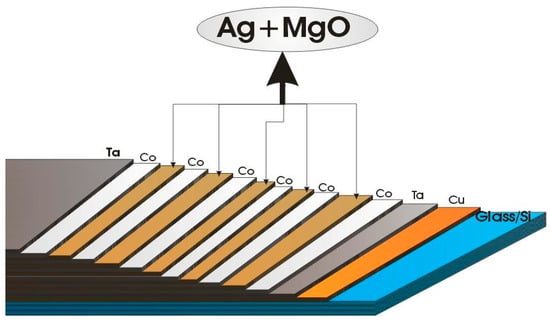
Figure 69.
The scheme of combined GMR-TMR deposition on silicon substrate.
This time the structure is represented by an alternative arrangement of cobalt single layers, as magnetic metal, and a mixture of silver and magnesium oxide layer as a nonmagnetic conductive + insulator layer.
The cross section of this structure together with the magneto-resistive effect measurement connections are given in Figure 70.
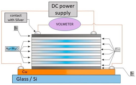
Figure 70.
A GMR-TMR granular-multilayer structure. Reprinted with permission from Ref. [40]. © 2011, Romanian Academy Publishing House.
The correspondent dependence of the structure resistance against the applied magnetic field is plotted in Figure 71 [12].
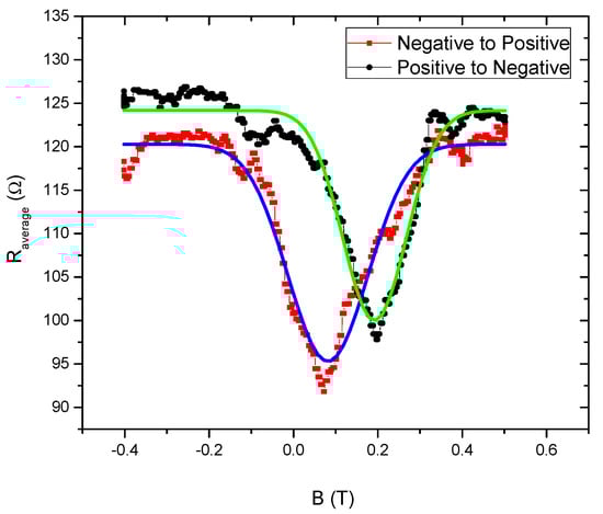
Figure 71.
Resistance of Ta/Cu/Co/(Ag + MgO)/Co/Ta structure against magnetic field induction.
From the given figure, one can see that the resistance of the structure is higher than in GMR cases and lower than in TMR cases.
This can give the possibility to deposit layers with desired resistance in function of insulator concentration which can find interesting future applications.
11. Conclusions
The thermionic vacuum discharge technology of thin layer deposition is a less known technology by the scientific community. For this reason, the authors found it worthwhile to present this method in English in order to highlight its advantages and to promote TVC technology as an interesting alternative to other many deposition technologies.
Its advantages can be summarized as follows:
- -
- It is carried out in high, very high or, if possible, in ultra-very high vacuum conditions with no gas present;
- -
- The discharge equipment can be easily mounted in any adequate vacuum chamber, even as a complete modular set;
- -
- The cathode of discharge is a tungsten wire which is surrounded by a focusing cylinder—the Whenelt cylinder;
- -
- The discharge currents can be changed from a few hundred of mA to large arc currents of hundreds of A, when the Whenelt cylinder is also made of tungsten and is properly cooled;
- -
- The discharge anodes can have different forms as for example a rod, or rests of materials put in a crucible;
- -
- When working with low discharge/currents and high voltages, the electrical contacts are not as important since the necessary power is obtained by using high voltages and no high currents; (this may be a disadvantage from the work security conditions);
For very low currents, the evaporation can be made only by electron bombardment as in classical procedures;
There are many variable parameters useful for process monitoring: filament heating current, anode-cathode distance, variable cathode axis orientation in case of electron gun structure, anode potential, load resistance;
- -
- Possibility to use two distinct arrangements (electron gun, or ring cathode);
- -
- Possibility to produce high purity and well compacted deposition with the contribution of the genuine ion bombardment of the substrate, the ions energy being varied during the deposition from some tens of eV to some hundreds of eV and even more;
- -
- The low current discharges combined with very low sputtering yield of the tungsten makes it possible to lessen the deposit poisoning.
- -
- The layer purity can be improved when using very low discharge currents and exclusive surface evaporation of the anode rod when no crucible is necessary;
- -
- The evaporation sources being punctual (point) represents a serious advantage when carrying out many simultaneous discharges; in this case a lot of probes with continuously varying concentrations can be obtained at single run;
- -
- Possibility of depositing alternate layers by initiating alternate discharges in two independent vapors of depositing combined mixed layers by concurrent discharges or evaporation (without discharge);
- -
- Possibility to in situ monitor the desired concentrations by analyzing the discharge spectra.
Author Contributions
Conceptualization, I.M.; methodology, I.M. and I.J.; validation, C.P. and I.J.; investigation, C.P.; data curation, I.M. and I.J.; writing—original draft preparation, I.M.; writing—review and editing, I.J.; visualization, I.J. and C.P.; supervision, C.P.; project administration, C.L.; funding acquisition, C.L. All authors have read and agreed to the published version of the manuscript.
Funding
This work was supported by the National Authority for Research and Innovation in the frame of Nucleus programme—LAPLAS IV—contract 16N/2019 and by Romanian Ministry of Research, Innovation and Digitalization under Romanian National Core Program LAPLAS VII—contract no. 30N/2023.
Institutional Review Board Statement
Not applicable.
Informed Consent Statement
Not applicable.
Data Availability Statement
Not applicable.
Conflicts of Interest
The authors declare no conflict of interest.
References
- Badareu, E.; Popescu, I.I. Gaze Ionizate. In Ionized Gases; Editura Tehnica: Bucharest, Romania, 1965. (In Romanian) [Google Scholar]
- van der Ziel, A. Solid State Physical Elrctronics; Prentice Hall Inc.: Hoboken, NJ, USA, 1957. [Google Scholar]
- Kittel, C. Introduction to Solid State Physics; Wiley: Hoboken, NJ, USA, 1953. [Google Scholar]
- Nottingham, W.B.H. Thermionic Emission. In Electron Emission, Gasentladunge 1. PH 21; Springer: Berlin/Heidelberg, Germany, 1956. [Google Scholar]
- Moijes, B.I.; Pikus, G.E. Termoemissionnye Preobrezovateli I Nizkotemperaturnaiaq Plazma. In Thermoeission Convertors & Low Temperature Plasma; Izd. Nauka: Moscow, Russia, 1973. (In Russian) [Google Scholar]
- Chapman, S.; Cowling, T.G. The Mathematical Theory of Non-Uniform Gases; Cambrige University Press: Cambrige, UK, 1990. [Google Scholar]
- Mc Daniel, E.W. Collision Phenomena in Ionized Gases; Wiley: New York, NY, USA, 1964. [Google Scholar]
- Joseph, O.; Hirschfelder, C.F.; Curtiss, R. Byron Bird. In Molecular Theory of Gases & Liquids; John and Wiley and Sons: Hoboken, NJ, USA, 1954. [Google Scholar]
- Zvorykin, V.K. Electron Optics and Electron Microscope; John Wiley & Sons: New York, NY, USA, 1948. [Google Scholar]
- Titeica, S. Termodinamica. In Thermodinamics; Academiei: Bucharest, Romania, 1982. (In Romanian) [Google Scholar]
- Musa, G.; Popescu, A.; Mustata, I.; Ehrich, H.; Popescu, A.; Schuhmann, I. RING Cathode TVA-a Source of Pure Metal Vapors Plasma with Energetic Ions Content. In Proceedings of the Proc. ESCAMPIC 96, Poprad, Slovakia, 27–30 August 1996; p. 357. [Google Scholar]
- Jepu, I. Studiul Arcului Termionic in Vid pentru Obtinerea de Structuri Magneto-rezistive. (Thermionic Vacuum Arc Study for Obtaining Magneto-resistive Structures-In Romanian). Ph.D. Thesis, University of Bucharest, Bucharest, Romania, 2011. [Google Scholar]
- Roth, A. Vacuun Technology; North Holland: Amsterdam, The Netherlands, 1976. [Google Scholar]
- Kovalenko, V.F. Teplofiziceskie Protzesy i Elektrovakuumnye Pribory. In Themophysical Processes & Electrovacuum Devices; Sovetzkoe Radio: Moscow, Russia, 1975. (In Russian) [Google Scholar]
- Sree Harsha, K.S. Principles of Physical Vapor Deposition of Thin Films San Hose State University; Elsevier: San Diego, CA, USA, 2005. [Google Scholar]
- Mustata, I.; Biloiu, C. A Possible Way for dc Discharge Simulation. Control Plasma Phys. 1998, 38, 447–462. [Google Scholar] [CrossRef]
- Pitct, I. Einfuerungin die Theorie der Electronenoptik. In Introduction in the Electron Optics Theory; Barth: Leipzig, Germany, 1956. (In German) [Google Scholar]
- Serstiev, L.G. Elektronnaia optica i elektronnolucevye pribory. In Electron Optics &Electron Rays Devices; Mir Publishers: Moscow, Russia, 1971. (In Russian) [Google Scholar]
- Ehrich, E. The Anodic Vacuum Arc I. Basic Construction and Phenomenology. J. Vac. Sci. Technol. A 1988, 6, 134. [Google Scholar] [CrossRef]
- Brown, S.C. Basic Data of Plasma Physics; John Wiley & Sons Inc.: New York, NY, USA, 1959. [Google Scholar]
- Mustata, I.; Cretu, M.; Cudalbu, C.; Lungu, C.P.; Musa, G.; Ehrich, H.; Schuhmann, J.; Hegemann, T. The Discharge Energy Dependence of the Deposition Rate in TVA Technology. In Proceedings of the XXV-th ICPIG, Nagoya, Japan, 17–22 July 2001; p. 313. [Google Scholar]
- Mustata, I.; Cretu, M.; Cudalbu, C.; Lungu, C.P.; Musa, G.; Ehrich, H.; Schuhmann, J.; Hegeman, I. Deposition Rate as Described by the Electrioca Characteristics of TVA Discharges. Rom. Rep. Phys. 2002, 54, 259. [Google Scholar]
- Mausbach, M. Entwiklung eines Vskuumbogens zur Abscheidung von Cu-Schichten und Untersuchung der Korrelationen zwischen Plasmaparametern und Schichteingeschaften. Ph.D. Thesis, Development of one Vacuum Arc for Cu-Films Separation and the Study of Plasma Parameter Influence on Film Properties, Essen, Germany, 1994. (In German). [Google Scholar]
- Mustata, I.; Lungu, C.P.; Porosnicu, C.C.; Jepu, I.; Zaroschi, V. Descarcari Electrice in Gaze si Vapori. In Electrical Discharges in Gases and Vapors; Universala: Bucharest, Romania, 2012. (In Romanian) [Google Scholar]
- Liberman, A.; Lichtenberg, A. Principles of Plasma Discharges and Material Processing; John Wiley & Sons Inc.: Hoboken, NJ, USA, 1994. [Google Scholar]
- Anghel, A.; Mustata, I.; Porosnicu, C.; Lungu, C.P. Influence of the Bias Voltage on the Formation of the Beryllium Films by TVA Method. J. Nucl. Mater. 2009, 385, 242–245. [Google Scholar] [CrossRef]
- Lungu, C.P.; Mustata, I.; Porosnicu, C.; Anghel, A.; Jepu, I. Caracterizarea Filmelor Compozite Combinatoriale Obtinute prin Metoda TVA. In Characterization of Combinatorial Composite Films Obtained by TVA Method; Academia Oamenilol de Stiinta din Romania: Bucharest, Romania, 2010. (In Romanian) [Google Scholar]
- Ehrich, H.; Schuhmann, J.; Musa, G.; Popescu, A.; Mustata, I. Adhesive Metal Films Obtained by TVA Deposition. Thin Soliod Film. 1998, 333, 95. [Google Scholar] [CrossRef]
- Titeica, S. Mecanica Cuantica. In Quantum Mechanics; Academiei: Bucharest, Romania, 1984. (In Romanian) [Google Scholar]
- Pastor, G.M. Introduction to the Theory of Magnetic Nanostructures; Institute of Natural Sciences: Yakutsk, Russia.
- Ruderman, M.A.; Kittel, C. Indirect Exchange Coupling of Nuclear Magnetic Moments by Conduction Electrons. Phys. Rev. 1954, 96, 99. [Google Scholar] [CrossRef]
- Kosuya, T. A Theory of Metal Ferro and Anti-ferro-magnetism on Zener’s Model. Prog. Theor. Phys. 1956, 16, 16–57. [Google Scholar]
- McWeeny, R.; Sutcliffe, B.T. Methods of Molecular Quantum Mechanics; Academic Press: London, UK; Academic Press: New York, NY, USA, 1969. [Google Scholar]
- Wei, Z. Synthesis of Giant Magneto-Resistive Multilayers. Ph.D. Thesis, University of Virginia, Ann Arbor, MI, USA, 2001. [Google Scholar]
- Chen, S.-P.; Chang, C.-Y. Analytic Solutions of the Linear Boltzmann Transport Equation for Multi-Layered Systems. Phys. Rev. B 2005, 72, 064445. [Google Scholar] [CrossRef]
- Slonczewski, C. Conductance and Exchange Coupling of two Ferro-Magnets Separated by Tunneling Barrier. Phys. Rev. B 1989, 39, 6995–7002. [Google Scholar] [CrossRef]
- Teillet. Magnetisme et Materiaux Magnetiques. In Magnetism and Magnetic Materials; Universite de Rouen: Rouen, France. (In French)
- Binasch, G.; Grünberg, P.; Saurenbach, F.; Zinn, W. Enhanced Magneto-resistance in Layered Magnetic Structures with Antiferro-Magnetic Interlayer Exchange. Phys. Rev. B 1989, 39, 4828–4830. [Google Scholar] [CrossRef]
- Baibich, M.N.; Broto, J.M.; Fert, A.; Nguyen Van Dau, F.; Petroff, F.; Etienne, P.; Creuzet, G.; Friederich, A.; Chazelas, J. Giant Magnetgo-Resistance of (001)Fe/(001)Cr Magnetic Superlattices. Phys. Rev. Lett. 1988, 61, 2472–2474. [Google Scholar] [CrossRef] [PubMed]
- Jepu, I. Optimization of TVA Plasma for Multi-Layer GMR/TMR Film Preparation. Rom. Rep. Phys. 2010, 62, 771–779. [Google Scholar]
- Mustata, I.; Porosnicu, C.; Jepu, I.; Lungu, C.P. Simultaneous and Alternate thin Film Depositions by TVA Method. Rom. J. Phys. 2015, 60, 1525–1535. [Google Scholar]
- Răsleanu, D.; Ilie, D.; Ionescu, V.; Mocanu, V.; Mureşan, M.G.; OANCEA–STĂNESCU, I.M.; Ciupină, V.; Prodan, G.; Vasile, E.; Mustaţă, I.; et al. Thermionic vacuum Arc Deposited Cu and Co Nanostructured Multilayers Synthesis and Characterisation. J. Optoelectron. Adv. Mater. 2010, 12, 839. [Google Scholar]
- Kuncser, V.; Filoti, G.; Miculescu, F. Magnetic Properties of Fe-Co Ferro-magnetic Layers and Fe-Mn/Fe-Co Bilayers Obtained by RVA. J. Alloys Comp. 2010, 499, 23. [Google Scholar] [CrossRef]
- Mustata, I.; Lungu, C.P.; Lungu, A.M.; Zaroski, V.; Blideran, M.; Ciupina, V. Giant Magneto-resistive Granular Coating Prepared by TVA Method. Rom. J. Phys. 2004, 49, 499. [Google Scholar]
- Anghel, A.; Lungu, C.P.; Mustata, I.; Zaroschi, V.; Lungu, A.M.; Barbu, I.; Badulescu, M.; Pompilian, O.; Schinteie, G.; Predoi, D. GMR Coatings using Thermionic Vacuum Arc Technology. Czechoslov. J. Phys. 2006, 56, B16–B23. [Google Scholar] [CrossRef]
- Holderied, M.; Hackenbroich, B.; Micklitz, H. System atic Studies of TMR in Granular Films Made from well-defined Co Clusters. J. Magn. Magn. Mater. 2008, 231, 13. [Google Scholar] [CrossRef]
- Ionescu, V.; Osiac, M.; Lungu, C.P.; Pompilian, O.G.; Jepu, I.; Mustata, I.; Iacobescu, G.E. Morphological & Structural Investigations of Co-MgF2 Granular Thin Film Grown by TVA. Thin Sol. Films 2010, 518, 3945. [Google Scholar]
- Kuncser, V.; Mustata, I.; Lungu, C.P.; Lungu, A.M.; Zaroschi, V.; Keune, W.; Sahoo, B.; Stromberg, F.; Walterfang, M.; Ion, L.; et al. Fe-Cu Granular Thin Film with GMR by TVA Method Preparation and Structural Characterization. Surf. Coat. Technol. 2005, 200, 980. [Google Scholar] [CrossRef]
- Mustata, I.; Lungu, C.P.; Lungu, A.M.; Zaroski, V.; Blideran, M.; Ciupina, V. GMR Granular Layers Deposited by TVA Method. Vacuum 2004, 76, 131–134. [Google Scholar] [CrossRef]
- Bruno, P.; Chaspert, C. Ruderman-Kittel Theory of Oscillatory Interlayer Exchange Coupling. Phys. Rev. 1992, 46, 261. [Google Scholar] [CrossRef] [PubMed]
- Schiff, L.I. Quantum Mechanics; McGrow Hill: New York, NY, USA, 1949. [Google Scholar]
- Samal, D.; Anil Kumar, P.S. Giant Magnetoresistance. Resonance 2008, 13, 343–354. [Google Scholar] [CrossRef]
- Massey HS, W.; Burhop EH, S.; McDaniel, E.W. Electronic and Ionic Impact Phenomena. Am. J. Phys. 1970, 38, 551. [Google Scholar] [CrossRef]
- Reig, C. GMR & TMR Magneto-Resistance Sensors. From Phenomena to Applications. Available online: https://www.routledge.com/rsc/downloads/ch_2_9781315119595.pdf (accessed on 4 June 2018).
- Wang, C.; Guo, Z.; Rong, Y.; Hsu, T.Y. The effect of the size distribution on the giant magnetoresistance in magnetic granular. Phys. Stat. Sol. 2004, 241, 916–924. [Google Scholar] [CrossRef]
- Boll, R. Weichmagnetische Werkstoffe; Soft-Magnetic Material; Vacuum Melted; Vacuumgeschmeltze GMBH: Hanau, Germany, 1977. [Google Scholar]
- Kuncser, V.; Valeanu, M.; Schinteie, G.; Filoti, G.; Mustata, I.; Lungu, C.P.; Anghel, A.; Chiriac, H.; Vladoiu, R.; Bartolome, J. Exchange Bias and Spin Valve Systems with Fe-Mn Antiferro-magnetic Pinning Layers, Obtained by TVA. J. Magn. Magn. Mater. 2008, 320, 226. [Google Scholar] [CrossRef]
- Kuncser, V.; Tolea, F.; Schinteie, G.; Jepu, I.; Palade, P. The Effect of Hydrogenation on the Magnetic Properties of Layered Spin Valve Structures. Dig. J. Nanomater. Biostruct. 2011, 6, 199. [Google Scholar]
- Egelhoff, W.F.; Chen, P.J.; Powell, C.J.; McMichael, R.D.; Stiles, M.D. Surface and Interface Effects in the Growth of GMR Spin Valves for Ultrahigh Density Data Storage Applications. Prog. Surf. Sci. 2001, 67, 355. [Google Scholar] [CrossRef]
- Kanai, H.; Noma, K.; Hong, J. Advanced Spin Valve GMR Head. Fujitsu Sci. Technol. J. 2001, 37, 174. [Google Scholar]
- Anghel, A.; Porosnicu, C.; Badulescu, M.; Mustata, I.; Lungu, C.P.; Sugiyama, K.; Lindig, S.; Krieger, K.; Roth, J.; Nastuta, A.; et al. Surface morphology influence on deuterium retention in beryllium films prepared by thermionic vacuum arc method. Nucl. Instrum. Methods Phys. Res. Sect. B Beam Interact. Mater. At. 2009, 267, 426. [Google Scholar] [CrossRef]
- Jepu, I.; Porosnicu, C.; Mustata, I.; Lungu, C.P.; Kunkser, V.; Osiac, M.; Iacobescu, G.; Ionescu, V.; Tudor, T. Simultaneously TVA Discharges in Obtaining Ferro-magnetic Thin Films. Rom. Rep. Phys. 2011, 63, 804–816. [Google Scholar]
- Porosnicu, C.C. Optimizarea parametrilor de depunere pentru filmele subtiri obtinute prin prin metoda Arcului termionic in vid. In The TVA Obtained Thin Film Deposition Parameters Optimization; Faculty of Physics: Bucharest, Romania, 2008. (In Romanian) [Google Scholar]
- Porosnicu, C.C. Sinteza si caracterizarea filmelor de interes pentru fuziunea nucleara prin Metoda arcului termionic in vid. (Layers of Interest for Nuclear Fusion Deposited by TVA Method: Synthesis & Characterization). Ph.D. Thesis, University of Bucharest, Bucharest, Romania, 2011. [Google Scholar]
- Rubel, M.J.; Bailescu, V.; Coad, J.P.; Hirai, T.; Likonen, J.; Linke, J.; Lungu, C.P.; Matthews, G.F.; Pedrick, L.; Riccardo, V.; et al. Beryllium–Plasma Facing Components for the ITER-like Wall Project at JET. J. Phys. Conf. Series L 2008, 100, 062028. [Google Scholar] [CrossRef]
- Maier, H.; Hirai, T.; Rubel, M.; Neu, R.; Mertens, P.H.; Greuner, H.; Hopf, C.H.; Matthews, G.F.; Neubauer, O.; Piazza, G.; et al. Tungsten & Beryllium Armour Development for the JET-ITER-like Wall Project. Nucl. Fusion 2007, 47, 222. [Google Scholar]
- Marcu, A.; Ticoş, C.M.; Grigoriu, C.; Jepu, I.; Porosnicu, C.; Lungu, A.M.; Lungu, C.P. Simultaneous Carbon and Tungsten Thin Film Deposition using two TVA-s. Sol. Film. 2001, 519, 4074. [Google Scholar] [CrossRef]
- Musa, G.; Mustata, I.; Lungu, C.P.; Surdu-Bob, C.C.; Lungu, A.M.; Vladoiu, R.; Ciupina, V.; Bursikova, V. Refractory Metal Film Deposition by TVA Method. In Proceedings of the ISPC, Toronto, ON, Canada, 7–12 August 2005. [Google Scholar]
- Mustata, I.; Musa, G.; Blideran, M.; Zaroski, V.; Lungu, A.M.; Lungu, C.P.; Iwasaki, K. Ag-DLC Tribological Film Deposition by Double Thermionic Vacuum Arc. In Proceedings of the XXVII, ICPIG, Eindhoven, The Netherlands, 17–22 July 2005; Volume 4, p. 87. [Google Scholar]
- Kuncser, V.; Palade, P.; Schinteie, G.; Sandu, S.G.; Trupina, L.; Lungu, G.A.; Gheorghe, N.G.; Teodorescu, C.M.; Porosnicu, C.; Jepu, I.; et al. Interface characterization and atomic intermixing processes in Be/W bilayers deposited on Si(0 0 1) substrates with Fe buffer layers. J. Alloys Compd. 2012, 512, 199–206. [Google Scholar] [CrossRef]
- Lungu, C.P.; Porosnicu, C.; Jepu, I.; Lungu, M.; Marcu, A.; Luculescu, C.; Ticos, C.; Marin, A.; Grigorescu, C.E.A. The behavior of W, Be and C layers in interaction with plasma produced by terawatt laser beam pulses. Vacuum 2014, 110, 207–212. [Google Scholar] [CrossRef]
- Mateus, R.; Sequeira, M.C.; Porosnicu, C.; Lungu, C.P.; Hakola, A.; Alves, E. Thermal and chemical stability of the β-W2N nitride phase. Nucl. Mater. Energy 2017, 12, 462–467. [Google Scholar] [CrossRef]
- Jepu, I.; Baldwin, M.J.; Nishijima, D.; Doerner, R.P.; Porosnicu, C.; Lungu, C.P.; Dinca, P.; Marin, A. The influence of fusion-relevant D2-0.1He plasma on Be-W mixed-materials. J. Nucl. Mater. 2017, 484, 367–373. [Google Scholar] [CrossRef]
- Surdu-Bob, C.; Vladoiu, R.; Badulescu, M.; Musa, G. Control over sp2/sp3 Ratio by Tuning Plasma Parameters of TVA. Diam. Relat. Mater. 2008, 17, 1625. [Google Scholar] [CrossRef]
- Lungu, C.P.; Mustata, I.; Musa, G.; Zaroschi, V.; Lungu, A.M.; Iwasaki, K. Low Friction Silver–DLC Coatings Prepared by Thernionic Vacuum Arc Method. Vacuum 2004, 76, 127. [Google Scholar] [CrossRef]
- Lungu, C.P.; Mustata, I.; Musa, G.; Lungu, A.M.; Brinza, O.; Moldovan, C.; Rotaru, C.; Iosub, R.; Sava, F.; Popescu, M.; et al. Unstressed Carbon-Metal films deposited by TVA Method. J. Optoelectron. Adv. Mater. 2006, 8, 74. [Google Scholar]
- Musa, G.; Mustata, I.; Ciupina, V.; Vladoiu, R.; Prodan, G.; Vasile, E.; Ehrich, H. Diamond-Like Nanostructured Carbon Films Deposition Using Thernionic Vacuum Arc. Diam. Relat. Mat. 2004, 13, 1398. [Google Scholar] [CrossRef]
- Lungu, C.P. Nano-structured Material Influence on DLC, a Tribologic Coating. Surf. Coat. Technol. 2005, 200, 198–202. [Google Scholar] [CrossRef]
- Musa, G.; Ciupina, V.; Lungu, C.P.; Mustata, I.; Ehrich, H.; Hegemann, T. Thermionic Vacuum Arc Carbon Plasma Generation for Hydrogen-fre Carbon Film Deposition. In Proceedings of the XXV ICPIG, Nagoya, Japan, 17–22 July 2001; Volume 3, p. 219. [Google Scholar]
- Lungu, C.P.; Grigorescu, C.E.A.; Rusu, M.I.; Jepu, I.; Porosnicu, C.; Lungu, A.M.; Feraru, I.D.; Savastru, D. Nanodiamond crystallites embedded in carbon films prepared by thermionic vacuum arc method. Diam. Relat. Mater. 2011, 20, 1061–1064. [Google Scholar] [CrossRef]
- Porosnicu, C.; Anghel, A.; Sugiyama, K.; Krieger, K.; Roth, J.; Lungu, C.P. Influence of beryllium carbide formation on deuterium retention and release. J. Nucl. Mater. 2011, 415, S713–S716. [Google Scholar] [CrossRef]
- Lungu, C.P.; Mustata, I.; Lungu, A.M.; Zaroschi, V.; Musa, G.; Iwanaga, I.; Tanaka, R.; Matsumura, Y.H.; Tanaka, H.; Oi, T.; et al. Influence of Rhenium on The Thermo-electron Emission from Thoriated Tungsten Cathode During Re Deposition by TVA Method. J. Optoelectron. Adv. Mater. 2005, 7, 2513. [Google Scholar]
- Lungu, C.P.; Mustata, I.; Musa, G.; Lungu, A.M.; Zaroschi, V.; Iwasaki, K.; Tanaka, R.; Matsumura, Y.; Iwanaga, I.; Tanaka, H.; et al. Formation of Nano-structured Re-Ni-Cr Diffusion Barrier Coating on Nb Super Alloys by TVA Method. Surf. Coat. Technol. 2005, 200, 399–402. [Google Scholar] [CrossRef]
- Lungu, C.P.; Mustata, I.; Zaroschi, V.; Lungu, A.M.; Anghel, A.; Chiru, P.; Rubel, M.; Coad, P.; Matthews, G.F. Beryllium coatings on metals for marker tiles at JET: Development of process and characterization of layers. Phys. Scr. 2007, T128, 157. [Google Scholar] [CrossRef]
- Anghel, A.; Porosnicu, C.; Lungu, C.P.; Sugiyama, K.; Krieger, C.; Roth, J. Influence of thermal treatment on beryllium/carbon formation and fuel retention. J. Nucl. Mater. 2011, 416, 9–12. [Google Scholar] [CrossRef]
- Nemanič, V.; Zajec, B.; Žumer, M.; Porosnicu, C.; Lungu, C.P. Hydrogen permeability of beryllium films prepared by the thermionic vacuum arc method. Fusion Eng. Des. 2011, 86, 2421–2424. [Google Scholar] [CrossRef]
- Mateus, R.; Carvalho, P.A.; Franco, N.; Alves, L.C.; Fonseca, M.; Porosnicu, C.; Lungu, C.P.; Alves, E. Formation and delamination of beryllium carbide films. J. Nucl. Mater. 2013, 442, S320–S324. [Google Scholar] [CrossRef]
- Sugiyama, K.; Porosnicu, C.; Jacob, W.; Roth, J.; Dürbeck, T.H.; Jepu, I.; Lungu, C.P. Study of deuterium retention in/release from ITER-relevant Be-containing mixed material layers implanted at elevated temperatures. J. Nucl. Mater. 2013, 438, S1113–S1116. [Google Scholar] [CrossRef]
- Zajec, B.; Nemanič, V.; Žumer, M.; Porosnicu, C.; Lungu, C.P. Hydrogen permeability through beryllium films and the impact of surface oxides. J. Nucl. Mater. 2013, 443, 185–194. [Google Scholar] [CrossRef]
- Schinteie, G.; Greculeasa, S.G.; Palade, P.; Lungu, G.A.; Porosnicu, C.; Jepu, I.; Lungu, C.P.; Filoti, G.; Kuncser, V. Effects of annealing in Be/W and Be/C bilayers deposited on Si(0 0 1) substrates with Fe buffer layers. J. Nucl. Mater. 2015, 457, 220–226. [Google Scholar] [CrossRef]
- Jepu, I.; Doerner, R.P.; Baldwin, M.J.; Porosnicu, C.; Lungu, C.P. Temperature influence on deuterium retention for Be–W mixed thin films prepared by Thermionic Vacuum Arc method exposed to PISCES B plasma. J. Nucl. Mater. 2015, 463, 983–988. [Google Scholar] [CrossRef]
- Založnik, A.; Markelj, S.; Čadež, I.; Pelicon, P.; Vavpetič, P.; Porosnicu, C.; Lungu, C.P. The influence of nitrogen co-deposition in mixed layers on deuterium retention and thermal desorption. J. Nucl. Mater. 2015, 467, 472–479. [Google Scholar] [CrossRef]
- Greculeasa, S.G.; Palade, P.; Schinteie, G.; Lungu, G.A.; Porosnicu, C.; Jepu, I.; Lungu, C.P.; Kuncser, V. Be/W and W/Be bilayers deposited on Si substrates with hydrogenated Fe-Cr and Fe-Cr-Al interlayers for plasma facing components. J. Nucl. Mater. 2016, 481, 73–80. [Google Scholar] [CrossRef]
- Sugiyama, K.; Porosnicu, C.; Jacob, W.; Jepu, I.; Lungu, C.P. Investigation of deuterium retention in/desorption from beryllium-containing mixed layers. Nucl. Mater. Energy 2016, 6, 1–9. [Google Scholar] [CrossRef]
- Mateus, R.; Hakola, A.; Tiron, V.; Porosnicu, C.; Lungu, C.P.; Alves, E. Study of deuterium retention in Be-W coatings with distinct roughness profiles. Fusion Eng. Des. 2019, 146, 303–307. [Google Scholar] [CrossRef]
- Kumar, M.; Makepeace, C.; Pardanaud, C.; Ferro, Y.; Hodille, E.; Martin, C.; Roubin, P.; Widdowson, A.; Dittmar, T.; Linsmeier, C.H.; et al. Identification of BeO and BeOxDy in melted zones of the JET Be limiter tiles: Raman study using comparison with laboratory samples. Nucl. Mater. Energy 2018, 17, 295–301. [Google Scholar] [CrossRef]
- Mateus, R.; Porosnicu, C.; Lungu, C.P.; Cruz, C.; Siketić, Z.; Bogdanović Radović, I.; Hakola, A.; Alves, E. WP PFC contributors; Analysis of retained deuterium on Be-based films: Ion implantation vs. in-situ loading. Nucl. Mater. Energy 2018, 17, 242–247. [Google Scholar] [CrossRef]
- Mateus, R.; Porosnicu, C.; Franco, N.; Carvalho, P.A.; Lungu, C.P.; Alves, E. Stability of beryllium coatings deposited on carbon under annealing up to 1073 K. Fusion Eng. Des. 2019, 146, 303–307. [Google Scholar] [CrossRef]
- Tiron, V.; Porosnicu, C.; Dinca, P.; Velicu, I.L.; Cristea, D.; Munteanu, D.; Révész, Á.; Stoian, G.; Lungu, C.P. Beryllium thin films deposited by thermionic vacuum arc for nuclear applications. Appl. Surf. Sci. 2019, 481, 327–336. [Google Scholar] [CrossRef]
- Musa, G.; Vladoiu, R.; Ciupina, V.; Lungu, C.P.; Mustata, I.; Pat, S.; Akan, T.; Ekem, N. Characteristics of Boron Thin Films Obtained by TVA Technology. J. Optoelectron. Adv. Mater. 2006, 8, 697. [Google Scholar]
- Musa, G.; Mustata, I.; Dinescu, G.; Bajeu, G.; Bajeu, G.; Raiciu, E. Evaporation Source for Inside Tubing Deposition with Protective Layers. J. Appl. Phys. 1992, 1, 2869. [Google Scholar] [CrossRef]
- Lungu, C.P.; Ionescu, V.; Osiac, M.; Cotarlan, C.; Pompilian, O.; Lungu, A.M.; Ciupina, V. Thermionic Vacuum Arc Deposited Al-doped Amorphous Nano composite Coatings. J. Non-Oxide Glasses 2009, 1, 175. [Google Scholar]
- Schuhmann, J. Metalisierung von Polymeren (Polymer Metallization-In German). Ph.D. Thesis, University of Duisburg-Essen, Duisburg, Germany, 2000. [Google Scholar]
- Lungu, C.P.; Lungu, A.M.; Chiru, P.; Pompilian, O.G.; Tudor, A.; Brescia, R. Low Friction Properties of Nano-structured C-Ni Films Prepared by TVA Method. Int. Surf. Sci. Eng. 2010, 4, 191. [Google Scholar] [CrossRef]
- Wildenberg, I.P.; Aberle, A. Polycrystalline Silicon Thin Film Solar Cells on ACT-Textured Glass Superstrates. Adv. Opto-Electron. 2007, 2007, 024584. [Google Scholar]
- Musa, G.; Popescu, A.; Mustata, I.; Salabas, A.; Cretu, M.; Leu, G.F.; Ehrich, H.; Schuhmann, J. Amorphous Silicon Deposition using TVA Technology. In Proceedings of the XIV, ISPC, Praha, Czech Republic, 1991. [Google Scholar]
- Matthews, G.F.; Edwards, P.; Hirai, T.; Kear, M.; Lioure, A.; Lomas, P.; Loving, A.; Lungu, C.; Maier, H.; Mertens, P.; et al. Overview of the ITER-like wall project. Phys. Scr. 2007, T128, 137. [Google Scholar] [CrossRef]
- Matthews, G.F.; Beurskens, M.; Brezinsek, S.; Groth, M.; Joffrin, E.; Loving, A.; Kear, M.; Mayoral, M.L.; Neu, R.; Prior, P.; et al. JET ITER-like wall—Overview and experimental programme. Phys. Scr. 2011, T145, 014001. [Google Scholar] [CrossRef]
- Matthews, G.F. JET EFDA Contributors, the ASDEX-Upgrade Team; Comparison of an ITER-like wall with a carbon wall in JET. J. Nucl. Mater. 2013, 438, S2. [Google Scholar] [CrossRef]
- Rubel, M.; Coad, J.P.; Widdowson, A.; Matthews, G.F.; Esser, H.G.; Hirai, T.; Likonen, J.; Linke, J.; Lungu, C.P.; Mayer, M.; et al. Overview of erosion–deposition diagnostic tools for the ITER-Like Wall in the JET tokamak. J. Nucl. Mater. 2013, 438, S1204–S1207. [Google Scholar] [CrossRef]
- Jepu, I.; Porosnicu, C.; Lungu, C.P.; Mustata, I.; Luculescu, C.; Kuncser, V.; Iacobescu, G.; Marin, A.; Ciupina, V. Combinatorial Fe–Co thin film magnetic structures obtained by thermionic vacuum arc method. Surf. Coat. Technol. 2013, 240, 344–352. [Google Scholar] [CrossRef][Green Version]
Disclaimer/Publisher’s Note: The statements, opinions and data contained in all publications are solely those of the individual author(s) and contributor(s) and not of MDPI and/or the editor(s). MDPI and/or the editor(s) disclaim responsibility for any injury to people or property resulting from any ideas, methods, instructions or products referred to in the content. |
© 2023 by the authors. Licensee MDPI, Basel, Switzerland. This article is an open access article distributed under the terms and conditions of the Creative Commons Attribution (CC BY) license (https://creativecommons.org/licenses/by/4.0/).