Article

Effects of Nitrogen Doping on Pulling Rate Range of Defect-Free Crystal in CZ Silicon

1
State Key Laboratory of Reliability and Intelligence of Electrical Equipment, Hebei University of Technology, Tianjin 300132, China
2
School of Materials Science and Engineering, Hebei University of Technology, Tianjin 300132, China
3
Zhonghuan Advanced Semiconductor Materials Co., Ltd., Yixing 214200, China
4
Hebei Engineering Laboratory of Photoelectronic Functional Crystals, Hebei University of Technology, Tianjin 300130, China
*
Authors to whom correspondence should be addressed.
Coatings 2023, 13(9), 1637; https://doi.org/10.3390/coatings13091637
Submission received: 19 August 2023 / Revised: 13 September 2023 / Accepted: 15 September 2023 / Published: 18 September 2023

Abstract

:
We investigated the effect of nitrogen doping on the pulling rate range of defect-free crystal in silicon with a diameter of 200 mm. It was found that the pulling rate range of defect-free crystal in nitrogen-doped Czochralski silicon is wider and the pulling rate (defect free) is lower than it is in non-nitrogen-doped Czochralski silicon. Under the experiment, the pull rate was from 0.67 mm/min~0.58 mm/min to 0.65 mm/min~0.54 mm/min. To further confirm the above experimental analysis, a numerical simulation process of nitrogen-doped Czochralski and non-nitrogen-doped Czochralski in an industrial system was performed. The V/G value along the S/L interface was the same for both models, but the distribution of Cvi (concentration of vacancy–concentration of self-interstitial) for nitrogen-doped Czochralski crystal silicon was more uniform and flat in a nitrogen-doped single crystal. Furthermore, the nitrogen-doped Czochralski crystal silicon had a smaller void size and a higher oxygen precipitation density. The experimental results are in good agreement with the numerical simulation results.

1. Introduction

In recent years, with the continuous revolution of device design, critical size is becoming smaller, which means that defects from the silicon crystal and wafer process are becoming increasingly stringent. Crystal originated particles (COPs) have become one of the key factors affecting device reliability, while process-induced defects that destroy the integrity of silicon wafers are another key factor. Shang Gao has studied the grinding and lapping-induced surface integrity of silicon wafers and its effects on chemical–mechanical polishing. Through their study, the surface morphology and subsurface damage generated by grinding and lapping were investigated, which helped chemical–mechanical polishing to achieve a polished wafer without foreign particles [1]. At the same time, when the size of COPs is equivalent to the design specification, device yield deterioration is encountered due to gate oxide failure and so on. Therefore, the coordination of COPs size must be considered in the production process, or, in the case of a strict device design, defect-free crystal will be required.
Several types of defects have been found in past years. Yuhong Zhao learned the relationship between the temperature gradient and secondary dendrites, which shows that the temperature gradient is a key factor in maintaining a stable solidification front and interface [2]. Under a stable solidification front and the interface condition, different types of intrinsic point defects (vacancy or self-interstitial) occur during crystal growth based on the V/G theoretical model (where V is the growth rate and G is the near-interface axial temperature gradient) [3]. The vacancy defect is dominant if V/G > the critical value; the vacancies accumulate to become V-defects during the crystal growth process [4]. The self-interstitial defect is dominant when V/G < the critical value; the self-interstitials accumulate to become I-defects after a more severe thermal process. When the V/G value intersects the critical value, the oxidation-induced stacking fault ring defect is prone to occur at this position. The vacancies and self-interstitials reach dynamic equilibrium when V/G is close to the critical value, which can be considered as the pulling rate range of defect-free crystal.
However, nitrogen and other impurities have important effects on the V/G critical value and COP accumulation. They can interplay with oxygen and vacancy to form different kinds of complexes and, furthermore, have a strong influence on the dynamics of microdefects during crystal growth [5]. Doping with donor concentrations above 1018 cm−3 can lead to both an increase or decrease of 0crit depending on the dopant atom size as the Fermi level effect is smaller than in p-type Si. The trapping of vacancies and the large binding energy is also the reason for the strong suppressing effect of nitrogen doping on the formation of COPs [6]. The impact of N on the vacancy and interstitial silicon intrinsic point defects is very important. Meanwhile, the N implication on the vacancy concentration is larger than it is on the interstitial silicon concentration, and this phenomenon becomes apparent when the N concentration is higher than the specified value [7]. NV (Nitrogen combined with Vacancy) and NO (Nitrogen combined with Oxygen) complexes exist simultaneously in nitrogen-doped Czochralski (NCZ) silicon. Nitrogen–vacancy (NV) and nitrogen–oxygen (NO) complexes compete in the nitrogen-doped Cz-Si crystals and their concentration fraction changes with [OI] value [8]. At present, nitrogen-doped Czochralski single-crystal technology has become popular in semiconductor silicon single-crystal. Infrared absorption experiments on the N-N-O defect in Si have been carried out. The involvement of both N and O in the defect is shown directly by observing N- and O-related isotopic shifts [9]. In the nitrogen-doped and fast-pulled crystals, the nitrogen plays a role in disturbing the growth of vacancy clusters by reducing the vacancy-rich region and the vacancy concentration. Therefore, the vacancy clustering is severely suppressed, and the increased residual vacancy causes anomalous oxygen precipitation [10]. Nitrogen doping could enhance the formation of grown-in oxygen precipitates in larger sizes at high temperatures via the complexes of N2–V2–OX, thus, leading to a significant loss of vacancies before the generation of voids during nitrogen-doped Czochralski crystal growth; on the other hand, the nitrogen doping could also enhance the formation of grown-in oxygen precipitates in smaller sizes at low temperatures via the complexes of Nm–On (Multiple Nitrogen and Oxygen combination). Thus, enhanced by nitrogen doping, the surviving vacancies in relatively lower concentrations resulted in denser voids with smaller sizes in the NCZ crystal [11]. It was believed that nitrogen doping could be an effective pathway for heavily P-doped CZ-Si to enhance oxygen precipitation, thus, increasing the internal gettering capability. Moreover, the nitrogen doping showed an enhancement effect on oxygen precipitation during the prolonged annealing with a rapid thermal processing pretreatment [12]. In nitrogen-doped crystals, the total amount of vacancies composing the voids increased during the crystal growth halt. These residual vacancies can enhance the formation of oxygen-precipitate nuclei during crystal growth [13]. Nitrogen in NCZ silicon enhanced the oxygen precipitation at lower temperatures, while it had no influence on the oxygen precipitation at higher temperatures. Meanwhile, nitrogen interacted with oxygen to form nitrogen–oxygen complexes as heterogeneous nuclei, which enhanced the nucleation of oxygen precipitates [14]. Nitrogen doping in a silicon crystal is known to have two main effects, the reduction in vacancy-related defects and the enhancement of oxygen precipitation. Nitrogen must have an important impact on the process window of COP free crystals based on a large number of research results from international scholars.
In this study, the effect of nitrogen doping on the pulling rate range of defect-free crystal in Czochralski silicon was investigated. A comparison of the formation behavior of various grown-in defects such as crystal-originated particles, and flow pattern defects, which occur in 200 mm diameter Cz-Si crystals grown under gradient pull rate conditions, with and without nitrogen doping, respectively, was performed.
At the same time, the V/G value of the S/L interface, Cvi (difference between voids and self-interstitials concentration), voids size, etc., were analyzed by numerical simulation and compared with the experimental results. Based on this study, the effect of nitrogen doping on the pulling rate range of defect-free crystal in Czochralski silicon can be discussed effectively.

2. Experimental Section

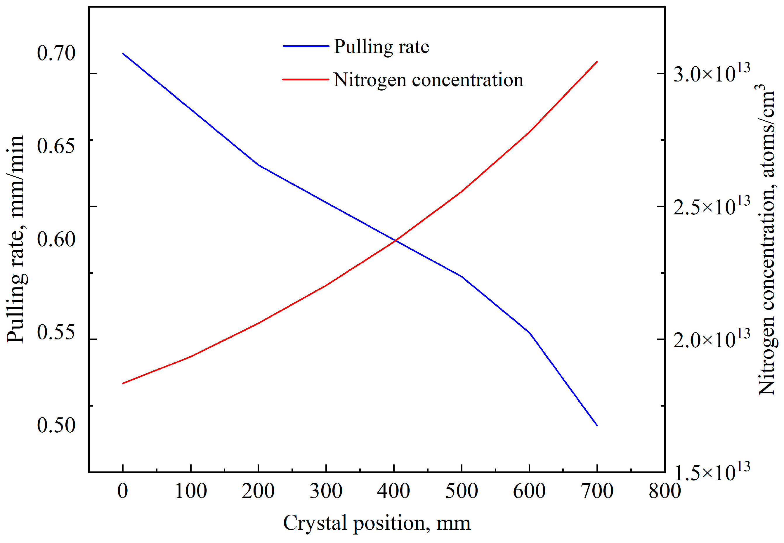
2.1. Experimental Details

In this experiment, a conventional 8-inch Czochralski single-crystal growth furnace was used, and the Czochralski furnace type was TDR110. To investigate the effects of nitrogen doping on the pulling rate range of defect-free crystal, two 200 mm (100) p-type silicon crystals were grown under almost the same conditions, besides nitrogen concentration, as shown in Table 1. The body length of the experimental single crystal was 700 mm, which was grown in a graphite thermal field of 24 inches, and the feeding volume was 180 kg.
As the pulling speed gradually changed from high to low, the crystal defect type mainly went through three stages, from V-rich (vacancy dominance) to V–I equilibrium (defect free), and then to I-rich (interstitial silicon dominance). Therefore, the experiment of gradually varying the pulling speed was performed to find the changes in the defect-free crystal (V–I equilibrium region) of non-nitrogen-doped Czochralski (CZ) silicon and nitrogen-doped Czochralski (NCZ) silicon, respectively. The pulling rate of the two crystals changed from 0.67 mm/min to 0.5 mm/min, as shown in Figure 1.
To obtain NCZ silicon, the silicon polish wafer with a silicon nitride epitaxial layer and polysilicon raw material was loaded into the quartz crucible. Then, nitrogen entered into the single-crystal silicon via the impurity segregation effect during the crystal growth process. The distribution of nitrogen was different in different crystal positions, which varied from low to high due to its low segregation coefficient, as shown in Figure 1. The nitrogen concentration in the grown crystal was calculated using the segregation coefficient of 0.0007 as it was difficult to measure the low nitrogen concentration in the silicon wafer. The common nitrogen concentration levels of the crystal growth in this experiment were approximately 1.9 × 10¹³ atoms/cm3 and 3 × 10¹³ atoms/cm3 at the starting position and the ending position, respectively.

2.2. Experimental Results and Discussions

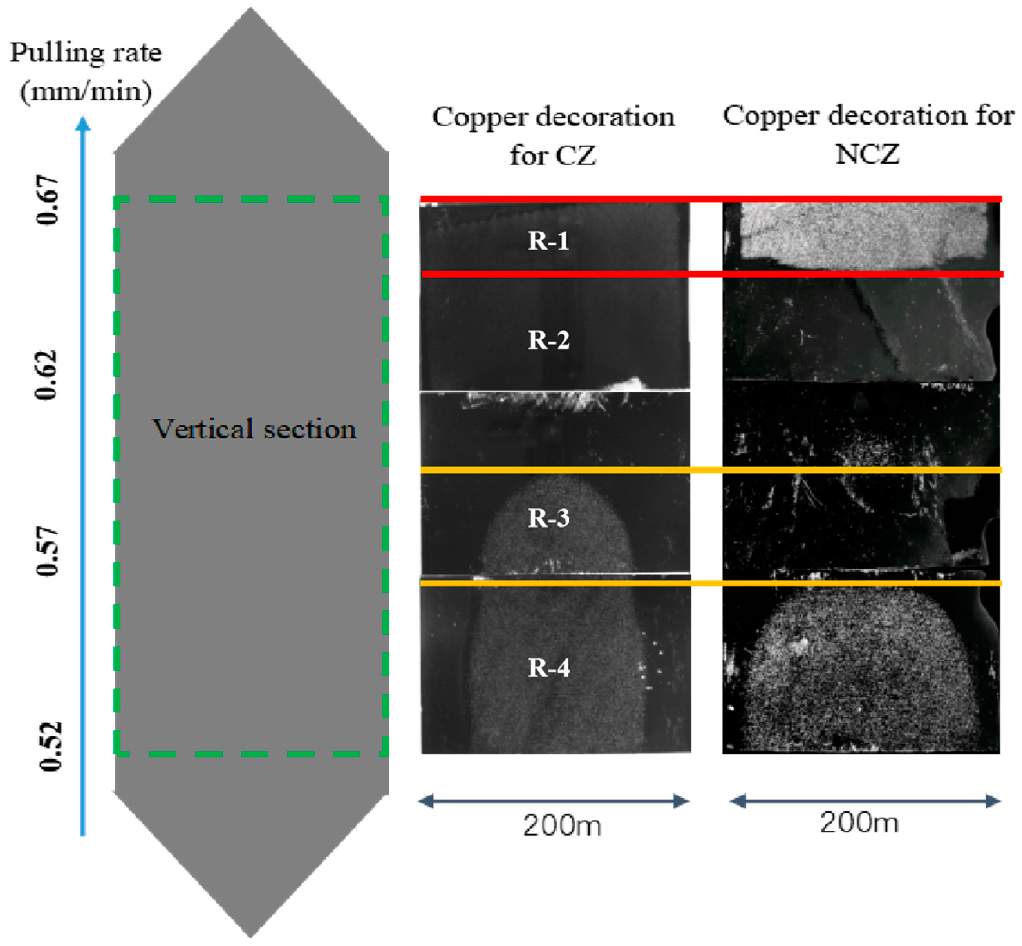
2.2.1. Copper Decoration Analysis

The properties of monocrystalline silicon are divided into three main categories depending on the pulling speed, including V-rich (vacancy dominance), V–I equilibrium (defect free), and I-rich (interstitial silicon dominance). Chemical etching is widely applied to decorate microdefects in monocrystalline silicon to qualitatively distinguish the crystal defect types. A general copper decoration technique has been widely used for qualitative analyses of crystal microdefect distribution, which is identified by saturating the wafer with copper at a high temperature followed by rapid cooling, allowing copper precipitate growth, followed by surface polishing and subsequent microdefect-decorating etching. In this experiment, the difference between CZ and NCZ defect-free windows was verified using copper decoration technology.
First, longitudinal sections were obtained from the CZ and NCZ silicon crystals by cutting along the axis. To obtain samples with a flat surface, the process of grinding and polishing was successively passed. Then, both groups of sample defects were tested using the cooper decoration technique [15,16]. The following steps were followed sequentially—(a) the two samples were coated uniformly on the back with high-concentration cupric nitrate (Cu(NO3)4·5H2O); (b) the two samples with copper nitrate were annealed at 900 °C for 10 min; (c) rapid cooling of the silicon wafer was performed to allow the heterogeneous nucleation of copper on the microdefects and subsequent growth of copper precipitate colonies; (d) chemical surface polishing was performed to clean the wafer surface; and (e) decorating etching was performed to decorate the copper precipitate colonies.
In the CZ silicon crystal, R-1 represents the near-defect-free crystal region, R-2 represents the defect-free crystal region, R-3 represents the low-density self-interstitial crystal region, and R-4 represents the I-rich crystal region. In NCZ silicon crystals, due to the influence of nitrogen on the distribution of defects, R-1 changed from near-defect-free to a V-rich crystal region, no change was observed in R-2, R-3 transformed from low-density self-interstitial to a defect-free crystal region, and R-4 represented a smaller I-rich region. As a result, the NCZ silicon crystals had a wider region of defect-free crystals.
According to Voronkov’s V/G (growth rate/temperature gradient), the type of point defect in a silicon crystal transforms from a vacancy to a self-interstitial atom as the growth rate decreases. For CZ silicon crystal, no V-defects are in the R-1 or R-2 areas with a pulling rate from 0.67 mm/min to 0.58 mm/min. I-defects are found when the pulling rate is below 0.58 mm/min, and dislocation loops or dislocation loop clusters form in R-3 through self-interstitial aggregation, which are identified as A-defects. Therefore, the pulling rate range of perfect crystal for CZ is from 0.67 mm/min to 0.58 mm/min, as shown in Figure 2.
For NCZ silicon crystal, the near-defect-free crystal is transformed into V-rich crystal in the R-1 region, and the I-rich crystal is transformed into a defect-free single crystal in the R-3 region. There are no V-defects in the R-2 and R-3 regions where the pulling rate is from 0.65 mm/min to 0.54 mm/min. I-defects are found when the pulling rate is below 0.54 mm/min, and dislocation loops or dislocation loop clusters form in R-3 through self-interstitials aggregation, which are identified as A-defects. Therefore, the pulling rate range of perfect crystal for NCZ is from 0.65 mm/min to 0.54 mm/min.

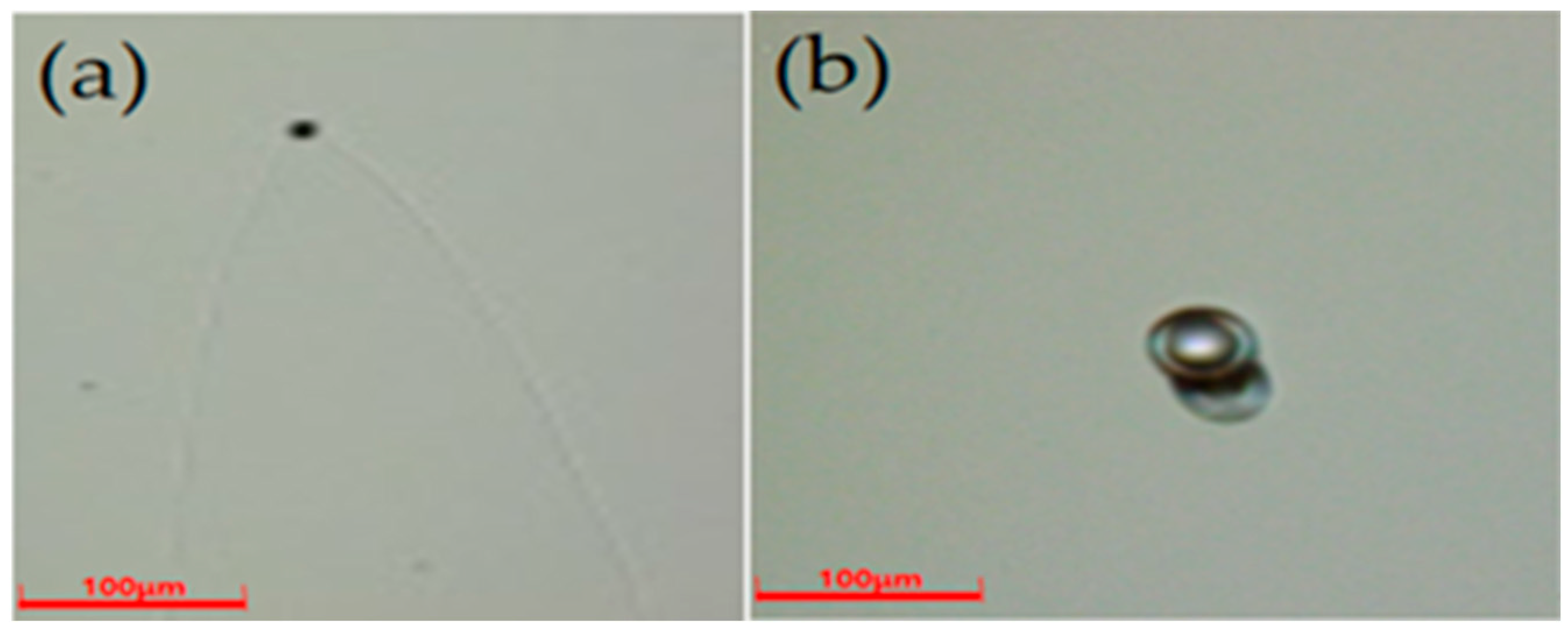
2.2.2. COPs and FPDs Analysis of Polish Wafer

To compare and analyze the results of copper decoration, experimental single-crystal ingots of CZ and NCZ were grown according to the original experimental boundary condition. The same position of the new experimental single-crystal ingots was then processed into a polish wafer. On the one hand, the particle distributions of the experimental CZ and NCZ polish wafers were tested using an SP2 device. On the other hand, the particle type (COPs or large dislocation particles (LDPs)) was tested using the flow pattern defect (FPD) technique [17,18] such that the samples were vertically immersed and etched in the Secco etchant (50%HF:0.15 mol/LK2Cr2O7 = 2:1) after polishing treatment. The morphology of the FPDs was observed using an optical microscope. The COP distributions of R-1, R-2, R-3, and R-4 for the CZ and NCZ silicon polish wafers were tested using the SP2 device. The distribution of COPs is shown in Table 2. The FPDs results map is shown in Figure 3.
Table 2 shows the COPs at 0.065 μm distribution maps detected by SP2 device. There are scattered COPs in the R-1 region from the CZ silicon crystal polish wafer. It was found that there are some agminated FPDs in the center of the R-1 samples from the CZ silicon polish wafer, like those shown in Figure 3a. The tip of the FPD is void, which could certify that these scattered particles are corresponding COPs. There are no FPDs on the edge of the CZ silicon polish wafer samples. The R-1 area should be a near-defect-free zone combined with the analysis of copper decoration results. At the same time, there are no COPs for the R-2, R-3, and R-4 regions, other particles should be foreign particles from the polishing process. There is no FPD, but there are some etch pits in the center of the R-3 and R-4 samples from the CZ silicon polish wafers. These etch pits are oval or twin etched pits from the FPD results of the R-3 and R-4 regions, like those shown in Figure 3b. These etch pits from the FPD test of R-3 and R-4 samples are LDPs (I-defects) which are in good agreement with the copper decoration results above and the numerical simulation results below.
There are a large number of COPs clustered in the central area in the R-1 region from the NCZ silicon crystal wafer. It was found that there are a large number of centrally aggregated FPDs in the center of the R-1 samples from the NCZ silicon polish wafers, like those shown in Figure 3a. Similar to the FPDs of the R-1 samples from the CZ silicon polish wafer samples, the tip of the FPD is void, which could certify that these scattered particles are also corresponding COPs. Meanwhile, there are no COPs for the R-2, R-3, and R-4 regions. Strangely, FPD test results showed that there are no FPDs or etch pits in the R-3 region of the NCZ samples, which is different from the FPD test results of the NCZ samples. Combined with the copper decoration results analysis, we believe the R-3 zone changed from an I-defect zone to a defect-free zone after nitrogen doping . However, etch pits (LDPs) were still found in the R-4 region of the NCZ samples, like those shown in Figure 3b. The distribution of COPs and LDPs is in good agreement with the results of the copper decoration analysis.

3. Numerical Simulation Section

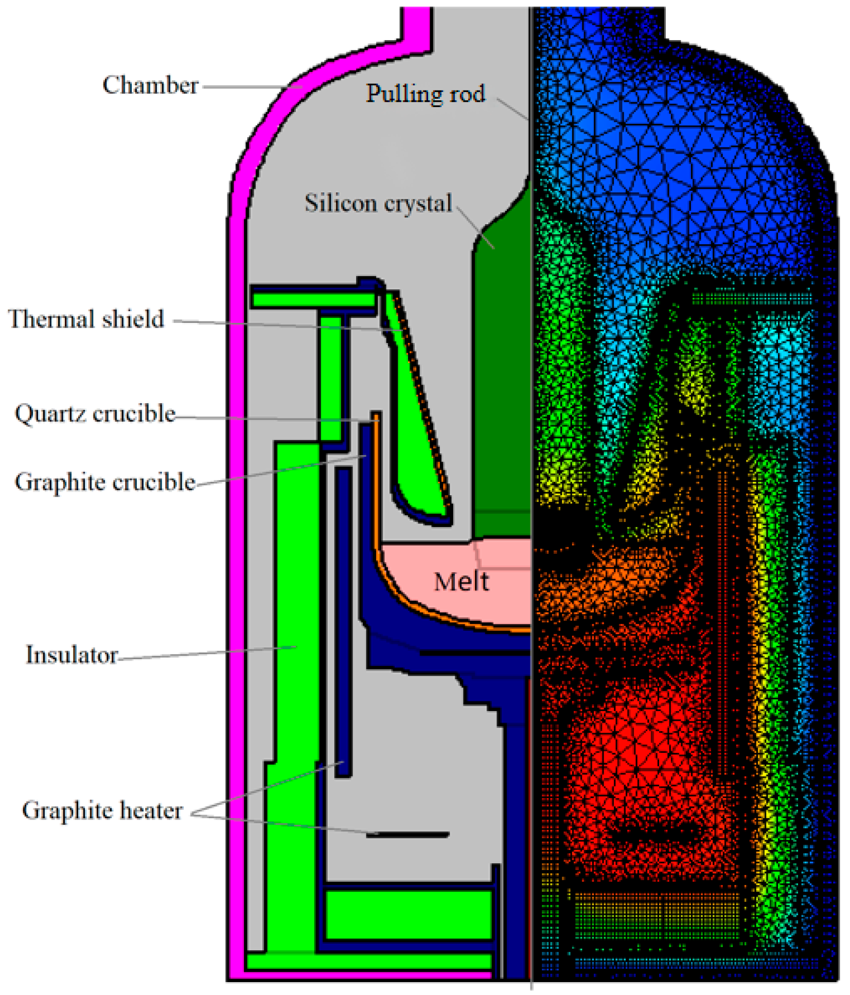
3.1. Numerical Simulation Setup

The agreement of CGSim simulations with experimental results has been extensively verified [19,20,21]. In this work, the CGSim (crystal growth simulator) program from STR Inc., which is based on the finite volume method (FVM), was used for all computations. Two-dimensional and three-dimensional steady-state simulations were performed with the basic module and flow module of the CGSim software package for computations of the global heat and mass transfer in the entire furnace, taking into account the turbulent convection in the melt and gas regions, the chemical mode of nitrogen doping, and the dynamics of intrinsic point defects in the crystal. The process of numerical simulation is mainly divided into three parts—(1) build the properties and formulas of the model filling materials and define each boundary combined with the process parameters; (2) construct the required crystal position (CP) locations, divide the grids, and adjust the encryption of the structured and unstructured grids and laminar flow grids; and (3) set the GUI operation, set the model solving conditions, add the required chemicals, and define the process parameter variables. The grid creation mainly consists of two modules—automatic grid division and manual grid modification. First, we used the automatic grid division function to automatically divide gas, solid, and liquid grids and generate unstructured grids. Then, we used the manual grid modification function to modify the solid–liquid interface of crystal and melt square area, we also modified the heat source conduction part into structured grids.The result is shown in Figure 4. Finally, the small mass and heat transfer space, crystal melt phase transition interface, gas–liquid intersection interface, and gas–solid boundary interface were mesh-corresponded. The problem of crystallization front correction requires a special grid design—the melt and the crystal should have a block with a quadrangular grid, which contains the melt–crystal interface. Boundary conditions should be set on different tabs separately; radiation, gas, and solid tabs should be used. External and internal subtabs are for external and internal boundaries, respectively. A special subtab with gas is proposed for boundary conditions to be set on boundaries between solid blocks and gas. Melt density (RHO) is supposed to be temperature-dependent to take into account the natural convection of the melt. At the same time, the defect simulation analysis is based on the steady-state heat and mass transfer simulation, and the whole crystal region needs to be structured with mesh encryption to ensure that the defect iteration can converge. Here, we discuss the effects of nitrogen doping on the distributions of the V and I concentrations and the V/G value along the S/L interface in a growing Si crystal.

3.2. V/G Value Based on the Different Growth Rates

To further confirm the above experimental analysis, we carried out a numerical simulation analysis using three pulling rates, 0.67 mm/min, 0.65 mm/min, and 0.55 mm/min, at the crystal position of 600 mm using simulation software CGSim. As shown in Figure 5, the V/G value in the center and edge of the growth interface was smaller under the three conditions of pulling rate. The forced convection below the solid–liquid interface makes the temperature gradient of the solution at the center larger, resulting in a small V/G value at the center. Because the edge is close to the gas–solid–liquid triple point, the temperature loss there is large. Therefore, the temperature gradient at the edge surges, resulting in a smaller V/G value at the edge. When the pulling speed is 0.55 mm/min, the V/G value in the center is less than the critical value of 0.013 cm2/min*K [22], which proves that the self-interstitial silicon may appear in the center when the pulling rate is gradually reduced, which agrees with the experiment. When the pulling speed is 0.7 mm/min, all the V/G values except for the edge are higher than the critical value of 0.013 cm2/min*K. Meanwhile, COP defects appear on the wafer when the pulling speed continues to increase, which is in good agreement with the experimental results. When the pulling speed is 0.65 mm/min, except for the edge, the remaining V/G values are close to the critical value of 0.013 cm2/min*K. When the V/G value is close to the critical value of 0.013 cm2/min*K, we believe that the concentration of self-clearance and vacancy defects generated by the solid–liquid interface is the same. At this time, most of the self-clearance and vacancy can cancel each other through diffusion and recombination during crystal growth, so that the growth of defectless single crystals can be realized.

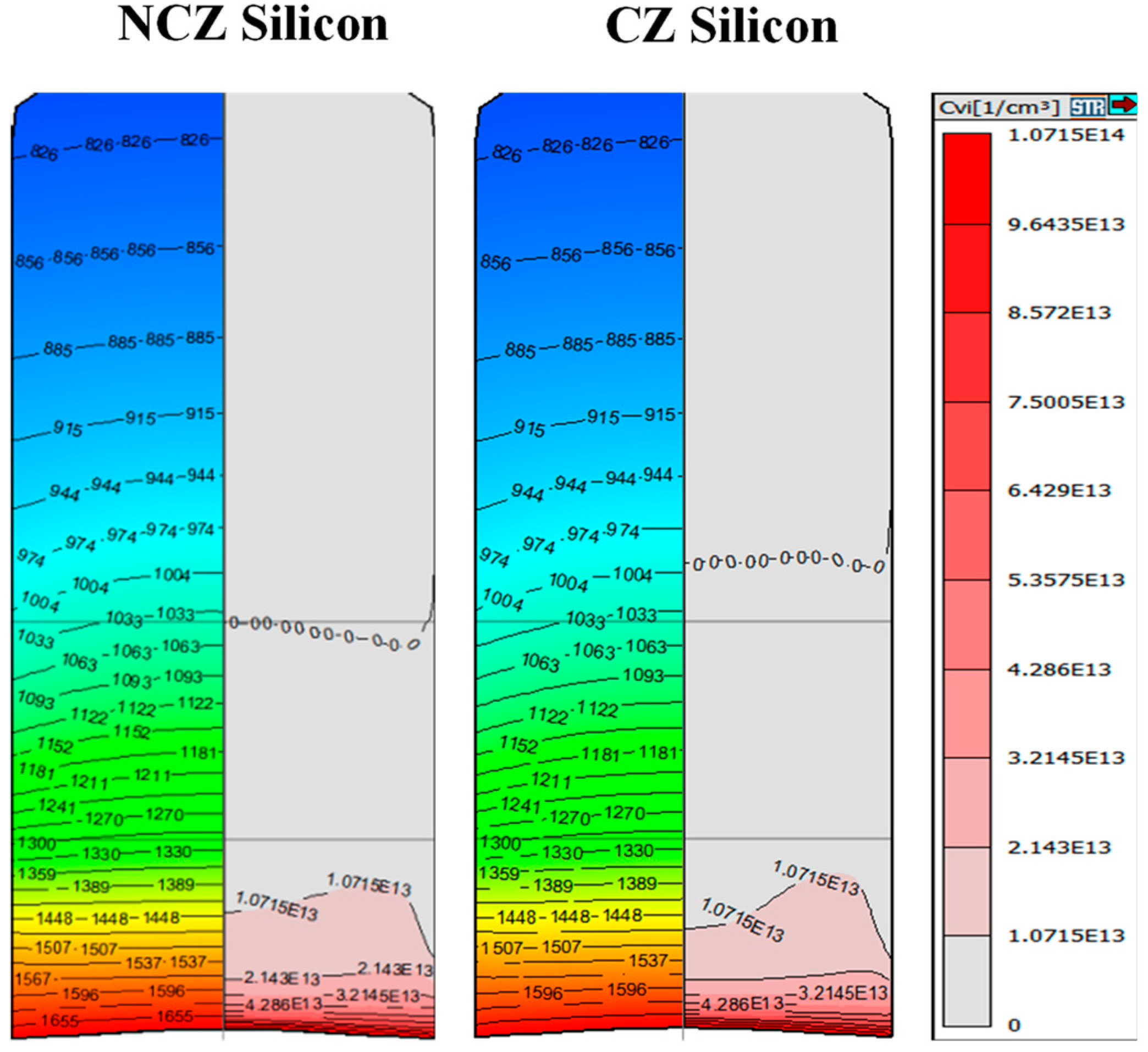
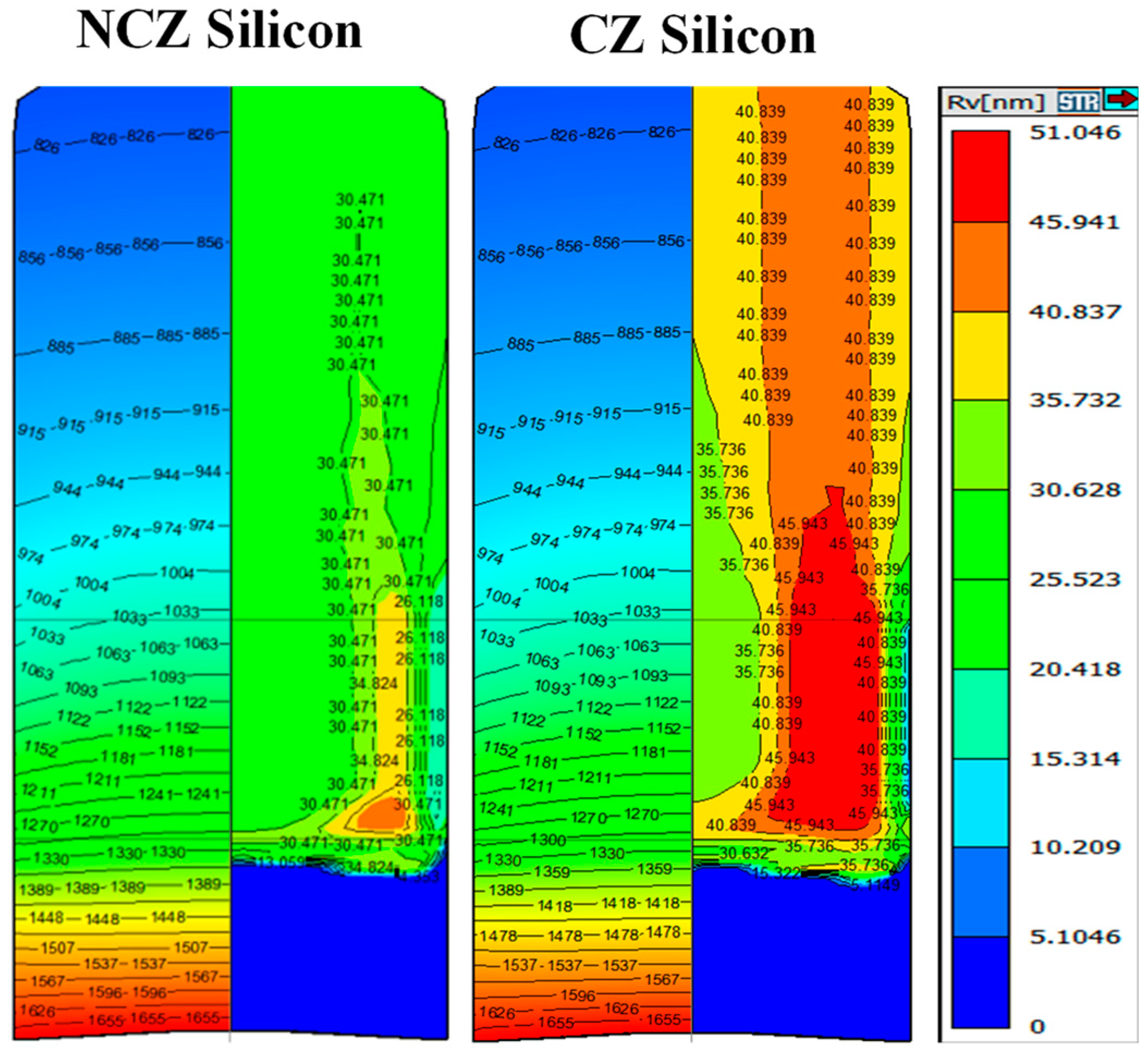
3.3. Defects for CZ and NCZ Crystal

There is a significant difference between the center and edge from the distribution of Cvi (concentration of vacancy–concentration of self-interstitial) for CZ crystal, as shown in Figure 6. Muhammad established six types of vacancy models in CrSI semiconductor monolayer [23], which helps us comprehend all the possibilities that vacancies can form and recombine into during the CZ crystal growth process. The internal temperature distribution of NCZ and CZ crystals is the same under the same pulling conditions. NCZ crystal promotes COP nucleation, resulting in an increase in COP density, but a decrease in COP size. As can be seen from Figure 6, when T = 1450 K, the center Cvi of NCZ crystal is 1.0715 × 10¹³ (1/cm3), which is significantly larger than the center Cvi of 1.0072 × 10¹³ (1/cm3) of CZ crystal. At the same time, more vacancies remain in the NCZ crystal, and these excess residual vacancies recombine with self-interstitial. As can be seen from Figure 6, when T = 1360 K, the edge Cvi of NCZ crystal is 9.5489 × 10¹² (1/cm3), which is significantly smaller than the center Cvi of 1.0693 × 10¹³ (1/cm3) of CZ crystal. The simulation results are in good agreement with the experimental results.
At the same time, the influence of different dopants on crystal particles is also different. Some dopants inhibit the growth of particles and increase their density, while some dopants increase the size of particles and reduce their density. The size of voids for NCZ crystal silicon is smaller than that for CZ crystal silicon, and its pore size is reduced by 15–20 nm, as shown in Figure 7. In NCZ crystal silicon, the combination of nitrogen, oxygen, and vacancy to form a bulk defect, will reduce the concentration of free vacancy, not only inhibiting the growth of COPs but also reducing the size of COPs. At the same time, according to the Cvi distribution in Figure 6, the Cvi near the edge is more convex, which means that the vacancy concentration in this part is larger and may generate larger voids, which is in good agreement with the void size distribution shown in Figure 7.
The density of oxygen precipitation in NCZ crystal silicon increased significantly and was higher than it was in CZ silicon, and the overall oxygen precipitate density increased by 0.5 × 10⁹ to 2 × 10⁹, as shown in Figure 8. The density of oxygen precipitates in the center of the NCZ crystal is approximately 2.2161 × 10⁹–4.4322 × 10⁹ (1/cm3), which is slightly higher than the concentration of oxygen precipitates in the center of the CZ crystal, 2.0816 × 10⁹–3.4694 × 10⁹ (1/cm3). At the same time, the density of oxygen precipitates at the edge of the NCZ crystal is approximately 2.9548 × 10⁹–6.6483 × 10⁹ (1/cm3), which is significantly higher than the concentration of oxygen precipitates at the center of the CZ crystal, 2.7755 × 10⁹–4.3945 × 10⁹ (1/cm3).
Nitrogen doping promotes the nucleation of oxygen precipitation due to the decrease in vacancy supersaturation but does not promote the growth of the void. Therefore, the size of the void decreases and the density increases. Excess vacancies, which remain in the crystals just after void formation, will recombine with interstitial silicon atoms or promote oxygen precipitation so that interstitial silicon atoms are reduced [24].
Through the comparative analysis of numerical simulation results, we believe that NCZ crystal silicon has better Cvi distribution than CZ crystal silicon, which is conducive to the diffusion and recombination of intrinsic point defects and further crystal improvement. At the same time, due to the effect of nitrogen on vacancy supersaturation, it can inhibit the production of large COPs. Because more vacancy remains in the growth process of NCZ crystal silicon than CZ crystal silicon, the concentration of oxygen precipitates inside the crystal can be increased to improve the internal impurity absorption capacity and mechanical strength of the chip to a certain extent.

4. Conclusions

We investigated the effect of nitrogen doping on the pulling rate range of defect-free crystal in Czochralski (CZ) silicon. It was suggested that the pulling rate range of defect-free crystal silicon is from 0.67 mm/min~0.58 mm/min to 0.65 mm/min~0.54 mm/min. The near-defect-free crystal is transformed into V-rich in the R-1 region, and the I-rich crystal is transformed into a defect-free single crystal in the R-3 region. The simulation results show that the V/G value along the S/L interface is the same for NCZ and CZ models, but the distribution of Cvi (Cv-Ci) for NCZ crystal silicon is more uniform and flat in a nitrogen-doped single crystal. The size of voids in NCZ crystal silicon is smaller than that in CZ crystal silicon. The density of oxygen precipitation in NCZ crystal silicon increased significantly and was higher than it is in CZ silicon. The experimental results are in good agreement with the numerical simulation results. Based on the above results, on the one hand, nitrogen doping could enhance the formation of voids during crystal growth and residual vacancies could remain, on the other hand, the residual vacancies recombine with interstitial silicon or promote oxygen precipitation so that interstitial silicon atoms are reduced. The research in this paper provides some guidance and suggestions for the production of defect-free single-crystal technology with a high demand for internal gettering in the semiconductor silicon material industry.

Author Contributions

Formal analysis, Z.L., Z.X. and G.C.; Data curation, Z.L.; Writing—original draft, C.S., X.A., H.Z. and G.C.; Writing—review & editing, H.Z., Z.L. and G.C. All authors have read and agreed to the published version of the manuscript.

Funding

This work was supported by the project for the Science and Technology Correspondent of Tianjin City (Grant No. 20YDTPJC01710) and the Research Foundation of Education Bureau of Hebei (Grant No. QN2021044).

Institutional Review Board Statement

Not applicable.

Informed Consent Statement

Not applicable.

Data Availability Statement

Not applicable.

Conflicts of Interest

The authors declare no conflict of interest.

References

  1. Gao, S.; Li, H.; Huang, H.; Kang, R. Grinding and Lapping Induced Surface Integrity of Silicon Wafers and Its Effect on Chemical Mechanical Polishing. Appl. Surf. Sci. 2022, 599, 153982. [Google Scholar] [CrossRef]
  2. Zhao, Y.; Zhang, B.; Hou, H.; Chen, W.; Wang, M. Phase-Field Simulation for the Evolution of Solid/Liquid Interface Front in Directional Solidification Process. J. Mater. Sci. Technol. 2019, 35, 1044–1052. [Google Scholar] [CrossRef]
  3. Voronkov, V. The mechanism of swirl defects formation in silicon. J. Cryst. Growth 1982, 59, 625–643. [Google Scholar] [CrossRef]
  4. Voronkov, V. Vacancy and self-interstitial concentration incorporated into growing silicon crystals. J. Appl. Phys 1999, 86, 5975–5982. [Google Scholar] [CrossRef]
  5. Yu, X.; Chen, J.; Ma, X.; Yang, D. Impurity engineering of Czochralski silicon. Mater. Sci. Eng. R Rep. 2013, 74, 1–33. [Google Scholar] [CrossRef]
  6. Vanhellemont, J.; Kamiyama, E.; Sueoka, K. Silicon Single Crystal Growth from a Melt: On the Impact of Dopants on the v/G Criterion. ECS J. Solid State Sci. Technol. 2013, 2, P166–P179. [Google Scholar] [CrossRef]
  7. Taniguchi, M.; Sueoka, K.; Hourai, M. Density Functional Theory Study on Concentration of Intrinsic Point Defects in Growing N-Doped Czochralski Si Crystal. J. Cryst. Growth 2021, 571, 126249. [Google Scholar] [CrossRef]
  8. Kajiwara, K.; Torigoe, K.; Harada, K.; Hourai, M.; Nishizawa, S. Oxygen concentration dependence of as-grown defect formation in nitrogen-doped Czochralski silicon single crystals. J. Cryst. Growth 2021, 570, 126236. [Google Scholar] [CrossRef]
  9. Berg Rasmussen, F.; Öberg, S.; Jones, R.; Ewels, C.; Goss, J.; Miro, J.; Deák, P. The nitrogen-pair oxygen defect in silicon. Mater. Sci. Eng. 1996, B36, 91–95. [Google Scholar] [CrossRef]
  10. Park, B.M.; Seo, G.H.; Kim, G. Nitrogen-Doping Effect in a Fast-Pulled Cz-Si Single Crystal. J. Cryst. Growth 2001, 222, 74–81. [Google Scholar] [CrossRef]
  11. Yu, X.; Yang, D.; Ma, X.; Yang, J.; Li, L.; Que, D. Grown-in Defects in Nitrogen-Doped Czochralski Silicon. J. Appl. Phys. 2002, 92, 188–194. [Google Scholar] [CrossRef]
  12. Zeng, Y.; Chen, J.; Ma, M.; Wang, W.; Yang, D. Enhancement effect of nitrogen co-doping on oxygen precipitation in heavily phosphorus-doped Czochralski silicon during high-temperature annealing. J. Cryst. Growth 2009, 311, 3273–3277. [Google Scholar] [CrossRef]
  13. Umeno, S.; Ono, T.; Tanaka, T.; Asayama, E.; Nishikawa, H.; Hourai, M.; Katahama, H.; Sano, M. Nitrogen Effect on Grown-in Defects in Czochralski Silicon Crystals. J. Cryst. Growth 2002, 236, 46–50. [Google Scholar] [CrossRef]
  14. Yang, D.; Ma, X.; Fan, R.; Zhang, J.; Li, L.; Que, D. Oxygen precipitation in nitrogen-doped Czochralski silicon. Phys. B Condens. Matter 1999, 273–274, 308–311. [Google Scholar] [CrossRef]
  15. Mule’Stagno, L. A Technique For Delineating Defects in Silicon. Solid State Phenom. 2002, 82–84, 753–758. [Google Scholar] [CrossRef]
  16. Kulkarni, M.S.; Libbert, J.; Keltner, S.; Muléstagno, L. A Theoretical and Experimental Analysis of Macrodecora-tion of Defects in Monocrystalline Silicon. J. Electrochem. Soc. 2002, 149, G153. [Google Scholar] [CrossRef]
  17. Zhang, J.; Liu, C.; Zhou, Q.; Wang, J.; Hao, Q.; Zhang, H.; Li, Y. Evolution of Flow Pattern Defects in Bo-ron-Doped <100> Czochralski Silicon Crystals during Secco Etching Procedure. J. Cryst. Growth 2004, 269, 310–316. [Google Scholar] [CrossRef]
  18. Xu, W.; Chen, J.; Ma XYang, D.; Gong, L.; Tian, D. Flow pattern defects in germanium-doped Czochralski silicon crystals. Appl. Phys. A 2011, 104, 349–355. [Google Scholar] [CrossRef]
  19. Chen, J.-C.; Chiang, P.-Y.; Nguyen, T.H.T.; Hu, C.; Chen, C.-H.; Liu, C.-C. Numerical Simulation of the Oxygen Concentration Distribution in Silicon Melt for Different Crystal Lengths during Czochralski Growth with a Trans-verse Magnetic Field. J. Cryst. Growth 2016, 452, 6–11. [Google Scholar] [CrossRef]
  20. Mukaiyama, Y.; Sueoka, K.; Maeda, S.; Iizuka, M.; Mamedov, V.M. Numerical Analysis of Effect of Thermal Stress Depending on Pulling Rate on Behavior of Intrinsic Point Defects in Large-Diameter Si Crystal Grown by Czochralski Method. J. Cryst. Growth 2020, 531, 125334. [Google Scholar] [CrossRef]
  21. Nguyen, T.H.T.; Chen, J.C.; Hu, C.; Chen, C.H. Numerical Simulation of Heat and Mass Transfer during Czo-chralski Silicon Crystal Growth under the Application of Crystal-Crucible Counter- and Iso-Rotations. J. Cryst. Growth 2019, 507, 50–57. [Google Scholar] [CrossRef]
  22. Von Ammon, W.; Dornberger, E.; Oelkrug, H.; Weidner, H. The Dependence of Bulk Defects on the Axial Tem-perature Gradient of Silicon Crystals during Czochralski Growth. J. Cryst. Growth 1995, 151, 273–277. [Google Scholar] [CrossRef]
  23. Muhammad, I.; Ali, A.; Zhou, L.; Zhang, W.; Wong, P.K.J. Vacancy-Engineered Half-Metallicity and Magnetic Anisotropy in CrSI Semiconductor Monolayer. J. Alloys Compd. 2022, 909, 164797. [Google Scholar] [CrossRef]
  24. Von Ammon, W.; Hölzl, R.; Virbulis, J.; Dornberger, E.; Schmolke, R.; Gräf, D. The Impact of Nitrogen on the Defect Aggregation in Silicon. J. Cryst. Growth 2001, 226, 19–30. [Google Scholar] [CrossRef]
Figure 1. Experimental crystal pulling rate and nitrogen concentration.
Coatings 13 01637 g001
Figure 2. Cooper decoration mapping of longitudinal sections for CZ and NCZ crystal.
Coatings 13 01637 g002
Figure 3. COPs (a) and LDPs (b) using FPD method.
Coatings 13 01637 g003
Figure 4. Material arrangement (left) and computational grids (right) in a furnace.
Coatings 13 01637 g004
Figure 5. Distribution of V/G for different pulling rates.
Coatings 13 01637 g005
Figure 6. Cvi (Cv–Ci) distribution of CZ and NCZ crystal.
Coatings 13 01637 g006
Figure 7. Rv (V-defects size) of CZ and NCZ crystal.
Coatings 13 01637 g007
Figure 8. Density of oxygen precipitation for CZ and NCZ crystal.
Coatings 13 01637 g008
Table 1. Key experimental conditions of two crystals.
Crystal TypeNitrogen Concentration
(Atoms/cm3)
Pulling Rate (mm/min)Diameter, mm
CZ00.67→0.5200
NCZ1.9 × 1013~3 × 10130.67→0.5200
Table 2. COPs inspected by SP2 at 0.065 μm mapping for CZ and NCZ experiments.
R-1R-2R-3R-4
COP Distribution at 0.065 μm
(CZ)
Coatings 13 01637 i001Coatings 13 01637 i002Coatings 13 01637 i003Coatings 13 01637 i004
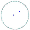
COP Distribution at 0.065 μm
(NCZ)
Coatings 13 01637 i005Coatings 13 01637 i006Coatings 13 01637 i007Coatings 13 01637 i008
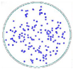
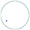
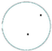
Disclaimer/Publisher’s Note: The statements, opinions and data contained in all publications are solely those of the individual author(s) and contributor(s) and not of MDPI and/or the editor(s). MDPI and/or the editor(s) disclaim responsibility for any injury to people or property resulting from any ideas, methods, instructions or products referred to in the content.

