Article

SrTiO3 Thin Films on Dielectric Substrates for Microwave Applications

1
Department of Physical Electronics and Technology, Saint Petersburg Electrotechnical University “LETI”, 197022 Saint Petersburg, Russia
2
Abram Fedorovich Ioffe Institute of Physics and Technology, Russian Academy of Sciences, 194021 Saint Petersburg, Russia
*
Author to whom correspondence should be addressed.
Coatings 2024, 14(1), 3; https://doi.org/10.3390/coatings14010003
Submission received: 27 November 2023 / Revised: 15 December 2023 / Accepted: 17 December 2023 / Published: 19 December 2023
(This article belongs to the Section Thin Films)

Abstract

:
Thin films of strontium titanate, which have nonlinear properties that are promising for microwave applications, were grown on a polycrystalline aluminum oxide substrate using magnetron sputtering and high-temperature annealing. It was shown that the improvement of the film structure with an increase in the deposition temperature was clearly correlated with both an increase in nonlinearity and an improvement in the loss level. A capacitor based on an SrTiO3 film deposited at a deposition temperature of 900 °C and subjected to annealing demonstrated a tunability of 46% with a loss tangent of 0.009–0.014 at a frequency of 2 GHz. This was the first successful attempt to form a planar SrTiO3 capacitor on an alumina substrate, which exhibited a commutation quality factor of above 3000 in the microwave range.

1. Introduction

The nonlinear dependence of the permittivity of ferroelectric (FE) materials on the external electric field makes them promising materials for microwave electronics. The use of thin films looks especially attractive due to the manufacturability of film materials, the ability to realize high levels of the control field in the film, and the possibility of integration with other microwave materials [1,2]. The advantages of film FE materials for microwaves include low losses, fast dielectric response, low power consumption, high operating power, and low manufacturing cost. It is possible to implement electrically tunable capacitors, phase shifters, delay lines, and other microwave elements using the dielectric nonlinearity of ferroelectric thin films [3,4,5].
To create a competitive microwave FE tunable element, the ferroelectric material must simultaneously exhibit high nonlinearity, low losses, low switching time (fast response), and have a weak dependence of properties on temperature [6]; these characteristics are difficult to combine in to one FE device. Let us take a closer look at this set of requirements.
The combination of high nonlinearity and low losses is determined by the commutation quality factor (CQF) of the element, which takes into account the tunability and loss tangent under the action of the control field [7,8]. In order to achieve high tunability, a FE material is usually selected, in which the temperature of the phase transition from ferroelectric to paraelectric state Tc is close to room temperature. This approach makes it possible to use a FE material with a maximum dielectric permittivity ε and, consequently, with a high nonlinearity [9]. Attempts to minimize losses in this case are reduced to the choice of a structurally matched single crystal substrate on which the oriented film is grown. As an example of such a choice, a film of a solid solution of barium and strontium titanates BaxSr1-xTiO3 (BST) for which a change in x from 0 to 1 allows varying Tc from 40 to 400 K, can be considered. A large number of works have been devoted to the study of the microwave properties of highly oriented BST films of composition x = 0.5–0.6 with a phase transition temperature close to 300 K grown on single crystal substrates [10,11,12]. The approach cannot be called optimal, since the proximity of the material’s Tc to room temperature provides a strong temperature dependence of the properties. Moreover, the disadvantages of the substrate selected according to the principle of structural matching (losses, hygroscopicity, fragility, cost) worsen the final characteristics of the device [13]. The best values of the CQF for today have been demonstrated on polycrystalline films [14,15]. In addition, in works where high nonlinear properties of BST films are demonstrated, as a rule, the issues of thermal stability and fast switching are not considered.
The fast response of the FE elements is largely determined by the presence of charged defects in the crystal lattice [16]. Oriented defect-free films demonstrate a switching time of ~10−8 s [17]. However, as a rule, an oriented FE film, which exhibits high nonlinearity and a low switching time, due to its ferroelectric nature, does not reveal temperature stability properties.
A promising method for increasing the temperature stability of FE elements is the use of gradient structures based on films of various component compositions [18]. Such films can be considered as a multilayer composition with different phase transition temperatures of each layer. The best results for today on the temperature stability of FE structures were published in [19]: the temperature coefficient of capacitance of two-layer elements based on BST films with a Ba content of 50% and 90% does not exceed 10−4 K−1 in the temperature range of (−25 ÷ 125) °C, which is comparable to the same value of semiconductor elements. It should be emphasized that the use of a multilayer structure, where transition layers inevitably occur on interfaces, increases device losses and switching time [20].
As a result, an analysis of the literature shows that in works devoted to the production and study of highly tunable FE elements, as a rule, no attention was paid to thermal stability. In works where multilayer thermostable FE structures were studied, data on increased losses compared with single-layer films were given, and data on the switching time of structures were not given. The search for the “optimal for microwave applications” FE material remains a challenging task. In this paper, we proposed considering strontium titanate as such a material.
Strontium titanate is an oxide of strontium and titanium with the chemical formula SrTiO3 (STO). At room temperature, it is a centrosymmetric paraelectric material with a perovskite structure. The SrTiO3 single crystal does not undergo a ferroelectric phase transition when the temperature drops to 0 K. In single crystals, the dielectric permittivity increases from 300 at room temperature to almost 24,000 at 4 K. In addition to high ε, STO has low dielectric losses (tanδ) and a nonlinear dependence of the dielectric permittivity on the electric field. It has been suggested that the ferroelectric transition in SrTiO3 is suppressed by quantum fluctuations [21]. More importantly, the central symmetry in the STO unit cell can be easily disrupted by external disturbances, which leads to the formation of an electric dipole and, consequently, ferroelectricity in the material [22]. Ferroelectricity in strontium titanate can be caused by a small amount of impurities, applied electric fields, and mechanical stress [23].
Thin STO films usually exhibit lower ε and higher dielectric losses than a single crystal. The reasons for this behavior may be “dead layers” at the film-substrate interface, defects such as oxygen vacancies and associated local polar regions, as well as mechanical stresses of the crystal lattice [24].
During film growth, the mismatch of the film and substrate lattices and differences in thermal expansion coefficients can cause phase transformations and create internal compression or tensile stresses. Due to the mechanical interaction with a much thicker substrate, the film is clamped in two directions, which can lead to anisotropy of dielectric properties, rotation of spontaneous polarization relative to the film plane, a change in Curie temperature and, consequently, a change in dielectric constant and losses [25].
According to the theoretical prediction of Pertsev et al. [26], ferroelectric anomalies caused by biaxial mechanical stresses were observed at room temperature in single-crystal STO films grown via molecular beam epitaxy on DyScO3 substrates [23,24]. In [24], nonlinear dielectric behavior was observed at room temperature, but when the temperature decreased to 77 K, a hysteresis loop with a large residual polarization developed. The appearance of a hysteresis loop confirmed that this system was indeed a relaxor ferroelectric. It was also shown in [23] that the dielectric behavior of the film smoothly changed from a nonlinear, to a hysteresis dielectric with a decrease in temperature. The high ε at room temperature in these films (about 7000 at a frequency of 10 GHz) and its sharp dependence on the electric field are interesting for instrument applications, despite the increased losses (tanδ = 0.2). However, the deformation-induced ferroelectric state in these STO films was achieved by using a DyScO3 substrate, which is too expensive and rare to be used in practical applications.
More common substrates such as MgO, Al2O3 and SrTiO3 were considered in [25]. The difference in thermal expansion coefficients between these substrates and the STO film was used to create tensile and compressive stresses that should affect the characteristics of the films. All studied STO films grown on various substrates demonstrated a hysteresis dependence of polarization on an electric field with a fairly similar coercive field at 100 Hz and 10 K. However, the nonlinearity of STO films on MgO/Pt was higher than that of STO films on Al2O3/Pt and SrTiO3/Pt substrates. For oriented STO films on MgO/Pt, the film lattice shrank upon cooling from the growth temperature due to a mismatch in thermal expansion coefficients, which led to tetragonal distortion. As a result, the dielectric properties of these films were improved, providing maximum polarization, permittivity, and tunability. For polycrystalline STO films on SrTiO3/Pt, and on Al2O3/Pt, the induced deformation was quite low and the out-of-plane dielectric constant was lower, due to the presence of dead layers and grain boundaries.
Thus, the ferroelectric state can be induced in strontium titanate films due to significant distortions of the crystal lattice both at cryogenic temperatures [23,25] and at 300 K [22,26], depending on the strength of stresses that can be created in the film. However, STO films are perspective for microwave applications precisely in the paraelectric state, when polarization in the material occurs only under the action of an applied external electric field; the absence of spontaneous polarization reduces losses that make it possible to develop STO nonlinear microwave devices with perspective characteristics [27,28].
As for dielectric properties, strontium titanate exhibited the best microwave loss characteristics among perovskites, which was expressed in the multiplication of the quality factor and the measurement frequency Qxf > 100,000 GHz [29,30]. In terms of the fast-switching parameter, STO films were significantly superior to the BST films (ns vs. µs) due to the lower defectiveness of the crystal lattice [16]. The temperature dependence of the properties of strontium titanate was significantly less than that of BST, since the material was in a paraelectric phase and did not experience phase transitions near to room temperature [31]. Despite the above advantages, until today, strontium titanate has not been considered as a material with a promising set of properties for microwave applications. The only characteristic by which STO films were inferior to BST films was nonlinearity. The substitution of Sr by Ba in a solid solution led to an increase in the dielectric constant and, consequently, tunability [4,9,13,32].
It should be noted that to date, the tunability of STO films, acceptable for microwave applications, has been demonstrated only in the plane-parallel design of the capacitive element, where a strontium titanate film was applied to a conductive electrode (metal-dielectric-metal design (MDM) [33] or to a pair of planar Pt electrodes (4-electrode design) [34], with the upper electrodes formed on the surface of the STO layer. This design makes it possible to realize high levels of the electric field in the gap of the capacitor at low control voltages and, consequently, to achieve high nonlinearity. However, it is complicated by the technology of its manufacture through the introduction of operations for applying and etching chemically resistant platinum layers. The main disadvantage of the plane-parallel design of the capacitive tunable element was the low operating power, which limits their use to small signal devices in low-power microwave systems [35]. One of the main advantages of FE materials in comparison to semiconductor elements, is the ability to work at high signal powers without distortion of the main characteristics. It can only be realized in a planar design, when the functional FE layer is grown on a dielectric substrate and the electrodes are formed on the surface of the FE film. There is an approach where high nonlinearity of STO films is achieved through strain engineering, where a highly stressed film is deposited on a dielectric substrate with significantly different lattice parameters, for example on DsScO3. However, all publications describing this approach noted a significant increase in losses [23,24,36,37].
Thus, planar tunable elements based on strontium titanate films have the desired combination of properties for microwave applications (high quality factor, thermal stability, operating power, and fast switching) in the case of the implementation of highly nonlinear elements based on structurally perfect STO films on a dielectric substrate. In connection with the above, the purpose of this work was to study the growth processes of STO films depending on technological conditions in order to obtain layers of a high structural quality on a dielectric substrate and to study the structural properties of films and the electrical characteristics of planar capacitive elements based on them for their further use in the tunable devices of high-power microwave systems.

2. Experiment

2.1. Sample Preparation

Thin films of strontium titanate were obtained on polycrystalline aluminum oxide substrates (15 × 15 × 0.5 mm) via radio frequency magnetron sputtering. The ceramic target of SrTiO3 stoichiometric composition with a diameter of 3″ was made from a mixture of presynthesized chemically pure SrCO3 and TiO2 powders at the St. Petersburg Institute “Ferrite-Domain”. Before the film deposition process, the vacuum chamber was evacuated to a residual pressure of 10−3 Pa. The films were synthesized at substrate temperatures Ts in the range of 600 to 900 °C. An Ar:O2 (3:1) mixture was used as the working gas. Island films were deposited for 20–100 s at a working gas pressure of 10 Pa. The deposition time of continuous films with a thickness of 500 nm was 4 h, while the pressure in the working chamber at the beginning of the deposition process was 10 Pa and decreased to 3 Pa during the first 30 min of the process. After deposition, continuous films were annealed at a temperature of 1000 °C in flowing oxygen for 2 h.

2.2. Structure Investigation

The structure of island films was studied via the method of the backscattering of helium ions with an initial energy of 227 keV (medium-energy ion scattering MEIS). The crystal structure and phase composition of continuous films was controlled via X-ray phase analysis (XRD) on the DRON-6 diffractometer on the Cu Kα1 emission spectral line (λ = 1.54 Å). The measurements were carried out in the angular diffraction range 2Ө from 20° to 60° with a scanning speed of 2°/min in continuous mode.

2.3. Electrical Measurements
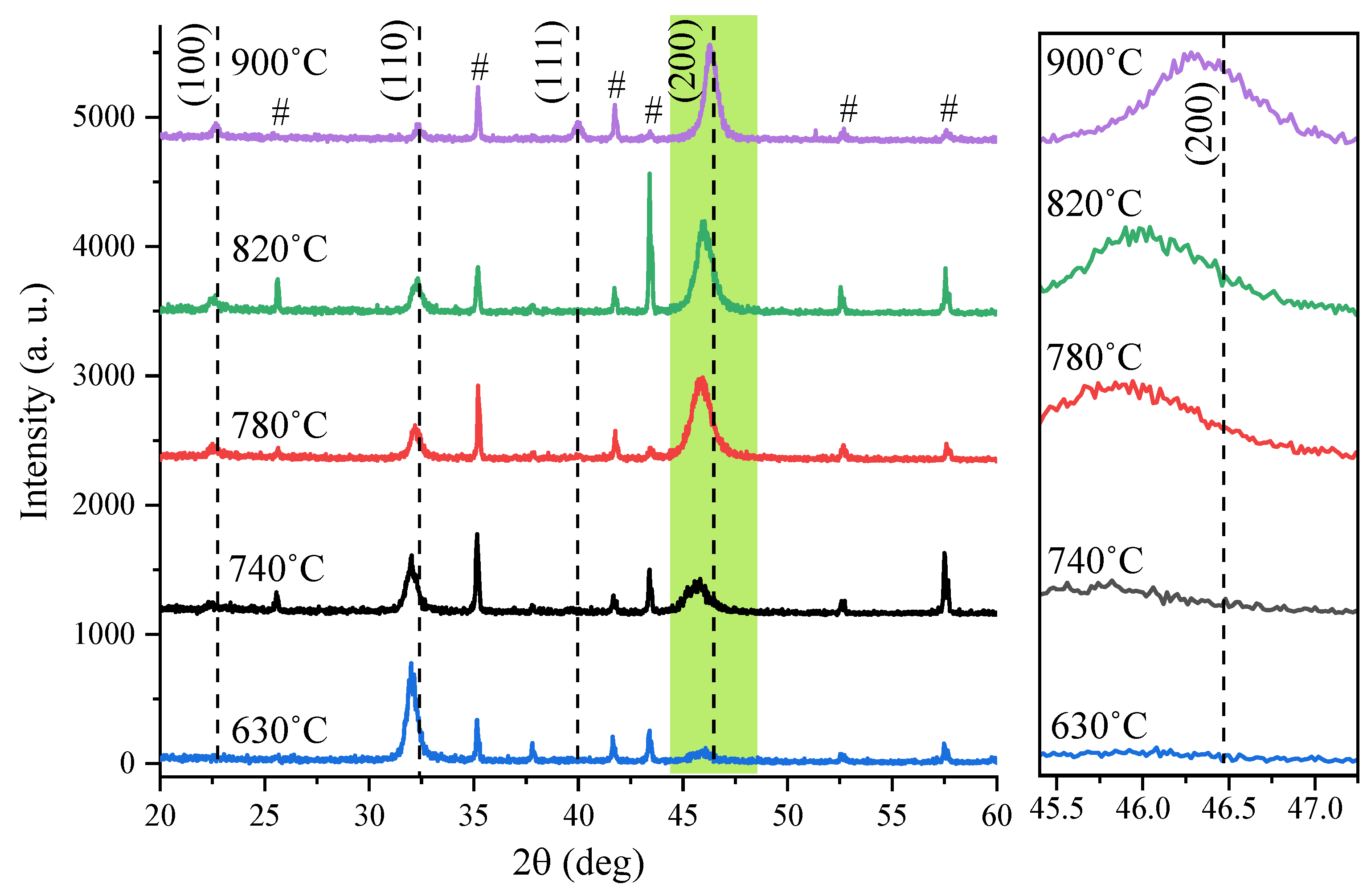
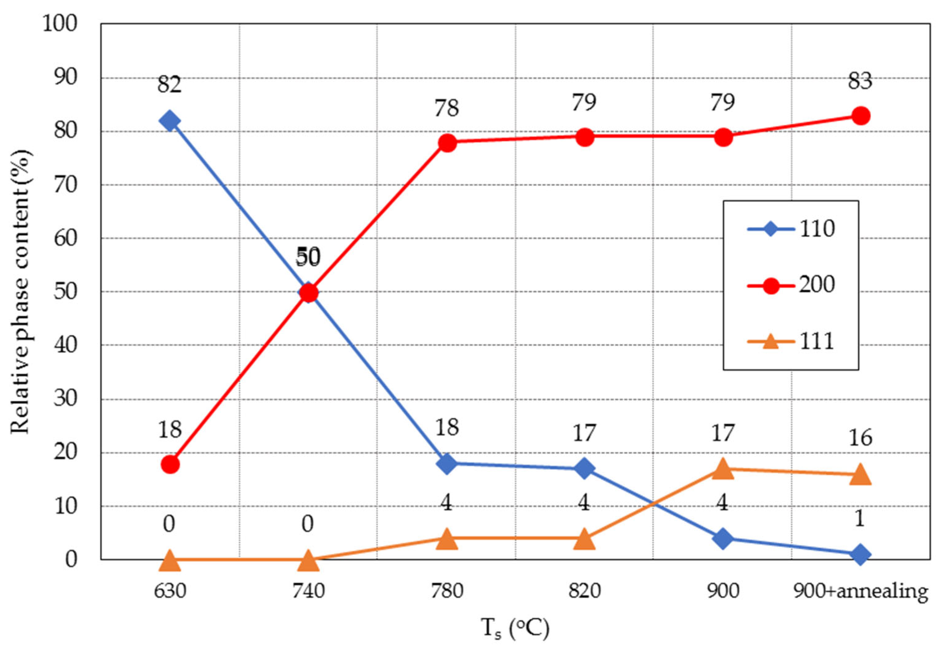
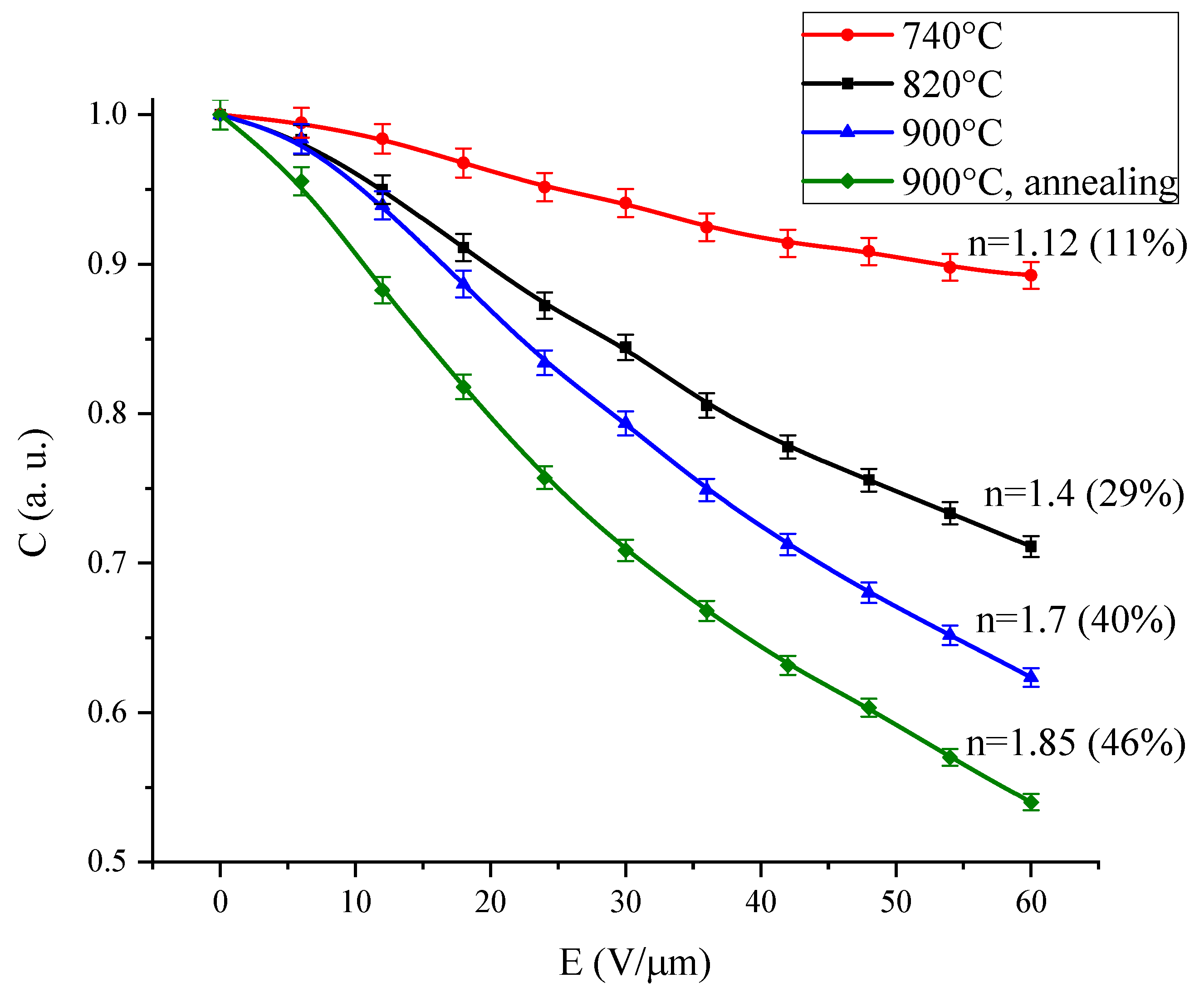
The electrical properties of STO films were studied using planar capacitors with the dimensions of 0.8 × 2 mm, and a gap width of 5 µm. Such dimensions provided a nominal capacitance of the capacitor of the order of 1 pF, suitable for microwave measurements. Copper electrodes were deposited on STO films via thermal evaporation using an adhesive chromium sublayer, followed by photolithography and chemical etching. Measurements of capacitance C and quality factor Q = 1/tanδ of capacitors were carried out at a frequency of f = 2 GHz using a half-wave stripline resonator and an HP 8719C vector analyzer. The resonator design provided an unloaded quality factor of 1000, which allowed for capacitance and a quality factor measurement accuracy of 1 and 5%, respectively. A control voltage of up to 300 V was supplied directly to the capacitor plates, providing an electric field strength in the capacitor gap of up to 60 V/μm. The tunability of the capacitors was calculated as the ratio of capacitances at zero and maximum applied control voltage n = C(0 V)/C(Umax), and also as n = (Cmax − Cmin)/Cmax.

3. Results

The mechanisms of nucleation of strontium titanate films on alumina substrates were studied using the MEIS method. The island films were bombarded with a beam of helium ions He+ with an energy of 227 keV; the energy of backscattered ions after interaction with film atoms was recorded via an electrostatic analyzer with a resolution of ΔE/E = 0.005. The energy spectra of backscattered ions from the STO island films deposited in the temperature range of 600 to 900 °C for 60 s, as well as spectra from films deposited at a temperature of 800 °C for 20, 40, 60, 80, and 100 s, were analyzed. Based on a comparison of experimental and model spectra, the geometry of the island, the area of the substrate covered by the film, and the elemental composition of the deposited coating were determined. Based on the shape of the peaks corresponding to the scattering of ions on individual elements of the film, the thickness of the coating and its deviation for each sample were determined. By comparing the intensities of the peaks and the signal from the substrate, the degree of the substrate covered by the film and the elemental composition were estimated [38].
The spectra of films deposited at different substrate temperatures did not differ significantly in shape, which indicated a single mechanism for the nucleation of strontium titanate films on an alumina in the deposition temperature range investigated [39]. As an example, Figure 1 shows experimental and simulated spectra of He+ ions after interaction with island films grown at temperatures of 800 °C and 900 °C. The parts of the spectra corresponding to the scattering of ions on strontium and titanium are triangular peaks with a prolonged low-energy front. As can be seen from the graph, an increase in the film deposition temperature did not lead to changes in the spectrum of backscattered ions, which indicated a similar geometric shape of the islands in the films under study. The asymmetrical triangular shape of the peaks indicated a significant deviation in the heights of the islands, the magnitude of which was comparable to the film thickness [40]. This shape of the spectrum corresponded to the process of island growth of the film according to the Volmer-Weber mechanism, which was realized at a weak interphase interaction between the film and the substrate [41].
Let us analyze the evolution of island films over time. Figure 2 shows the dependences of the thickness of the island films, as well as the surface area of the substrate occupied by the islands, on the deposition time. Table 1 shows data on the deposition time of the samples τ, the height of the islands h, the spread of heights σ, the ratio of the spread of heights to the height of the islands σ/h, the area of the substrate covered by the film C, and the total amount of substance on the substrate M. The values of h, σ, and M were obtained as a result of modeling MEIS spectra, where they were variable parameters of the iterative procedure; for details on the modeling technique see [38]. Here we note that the modeling was carried out in units of 1015 “united atoms”/cm2, where the “united atom” was a molecule of the form Sr0.2Ti0.2O0.6, i.e., a molecule, the sum of the indices of which was reduced to 1. Then the obtained values of h and σ were recalculated into nm based on the density of the material. Based on the analysis of the scattering spectra of He+ ions and the data of Table 1, the following conclusions can be drawn: (i) with increasing deposition time, the amount of substance on the substrate increases proportionally; (ii) the height of the islands h at the first stage increases from 2.5 to ~3.5 nm, then, with an almost constant film thickness, the degree of coverage of the substrate increases, i.e., the growth mechanism changes over time; (iii) the ratio of height scatter to island height σ/h decreases with increasing deposition time, which indicates a decrease in the surface relief of the STO film. By comparing the dynamics of changes in the height of the islands and the area occupied by them, the considered range of deposition times can be divided into three stages. The deposition time of 20 s corresponds to the nucleation stage, when individual islands of small height were formed on the surface of the substrate, occupying a small part of its area. The second stage (40–60 s), characterized by a significant increase in the area of the substrate occupied by islands, corresponded to the stage of coalescence, at which the islands merge with each other. The third stage (80–100 s) was the filling of voids between conglomerations of islands and the transition from the formation of islands to the growth of a continuous film [42].
Thus, based on the results of analysis of the initial stages of growth of strontium titanate films on a polycrystalline Al2O3 substrate, the following conclusions can be made. In the temperature range under study, nucleation and formation of the initial layers of the film occurred according to the Volmer-Weber island mechanism; individual islands of the STO phase were formed on the substrate, which then evolved into a continuous film without the formation of stressed transition layers [43]. During the deposition time of about 120 s, the film completely covered the substrate, the surface relief of the film was smoothed out, the stage of formation of the first continuous layer can be considered completed, and the next layer was formed on the strontium titanate itself. The technological conditions under which nucleation and formation of the initial STO layer occurred created the prerequisites for the growth of polycrystalline films. However, it is known that under certain conditions, the island growth mechanism of strontium titanate films can change to a layered form, providing an improvement in the crystal structure with an increase in film thickness [44].
Figure 3 shows comparative diffraction patterns of 500 nm thick STO films deposited at different substrate temperatures.
XRD analysis data allow us to conclude that the angular positions of the diffraction peaks corresponded to the structure of strontium titanate, and the interplanar distances in the direction normal to the surface of the STO film depended on the deposition temperature. The diffraction reflexes from STO films investigated were significantly broadened (FWHM ≅ 0.8°) compared to single-crystalline SrTiO3 (FWHM ≅ 0.3°). Films deposited at low substrate temperatures exhibited a polycrystalline strained structure with the main crystalline phase (110). As Ts increases, the X-ray reflections shifted toward larger angles, which indicated a decrease in internal stresses in the crystal lattice. In addition, an increase in the deposition temperature led to a change in the structure of the film from polycrystalline to (h00) predominantly oriented. Figure 4 shows comparative diffraction patterns of the film deposited at Ts = 900 °C before and after annealing in an oxygen environment at annealing temperature Tan = 1000 °C. The graph shows that the intensity of the main peak (200) increased by half an order of magnitude, and the width of the reflection decreased significantly, approaching the value for a single crystal (FWHM ≅ 0.4°).
The ratio of the main crystalline phases in films grown at different Ts, as well as under the influence of annealing, was estimated by comparing the intensities of experimental reflections normalized to the corresponding intensities of reflections from unstressed powder samples. For example, the fraction of (110) grains in a film can be estimated:
X ( 110 ) = I ( 110 ) I p ( 110 ) / I 100 I p 100 + I 110 I p 110 + I 111 I p 111 + I 200 I p 200 · 100 %
where I are the experimentally measured relative intensities of the (100), (110), (111) and (200) peaks, Ip are the corresponding relative integral peak intensities for powder samples. The calculation results are presented in Figure 5; the intensities of the reflections (100) and (200) are summed up in the calculation. A decrease in the relative intensity of the (110) peak with increasing film deposition temperature indicated a decrease in the relative volume of (110) oriented crystallites. For the film deposited at Ts = 900 °C, the intensity of the (200) reflection was more than 80% compared to the (110) and (111) reflections, i.e., the film became predominantly (h00) oriented.
The study of STO films via X-ray diffraction showed that in the deposition temperature range of 600 to 800 °C, polycrystalline films of strontium titanate, consisting of small strained crystallites, were formed on an alumina substrate. This situation is explained by the low mobility of adatoms at low Ts, as well as by substrate defects that act as numerous nucleation centers [43]. As the deposition temperature increased, the mobility of particles increased, which led to the nucleation of grains with minimal surface energy, and then to the formation of the (h00) predominantly oriented film with minimal internal stresses [41]. Annealing of an oriented film led to a significant enlargement of grain sizes and the almost complete elimination of internal stresses in the lattice.
Figure 6 and Figure 7 show the dependences of the capacitance normalized to the maximum value and the dielectric loss tangent of planar capacitors formed on the basis of various STO films on the control field strength. The figure shows that planar capacitors based on films deposited at low substrate temperatures demonstrated poor tunability (11% and 29% for Ts = 740 °C and 820 °C, respectively), which was due to the polycrystallinity and high defectiveness of these films. The improvement in film structure with increasing deposition temperature clearly correlated with both an increase in nonlinearity from 11% to 40% and an improvement in the loss level. The reason for the improvements was the predominantly oriented (h00) structure of the high-temperature film with minimal internal stress. The best electrical characteristics in terms of high tunability and low losses were demonstrated by capacitors based on film deposited at high temperature and subjected to annealing. In the film, there was a significant enlargement of the crystallites of the predominant phase, a decrease in the number of grain boundaries and an almost complete absence of internal stresses. The defect-free structure of the film provided a strong dependence of ε on the external field, and a reduction in losses. As a result, the capacitor based on the STO film deposited at Ts = 900 °C and subjected to annealing exhibited 46% tunability with a loss tangent of 0.009–0.014, which provided CQF = 3100.
The combination of high tunability and low losses required for successful microwave applications of FE elements was estimated through the commutation quality factor CQF, the value of which significantly depended on the frequency, which was due to the dependence of tanδ (f). A tunable FE element is considered promising for microwave applications if the CQF for it exceeds 1000 at the operating frequency [8]. Table 2 presents comparative data on tunability, losses, and the quality factor calculated from them for capacitors of various designs based on STO films. It follows from the data in the table that the planar capacitors obtained in this work demonstrate a promising quality factor in the microwave range. According to our data, this was the first successful attempt to form a planar STO capacitor on alumina substrate, which revealed CQF higher than 3000 at microwaves. Taking into account the ratio of electrophysical parameters (tunability and dielectric losses), and the cost of manufacturing a planar FE capacitor, this result looks promising for microwave applications. We plan to direct future research to improve the structure of STO films on an alumina substrate, and to study the microwave properties of STO planar capacitors in the aggregate: nonlinearity, losses, fast switching, and temperature stability.

4. Conclusions

Paraelectric strontium titanate films of good crystalline quality were obtained on a dielectric substrate of polycrystalline aluminum oxide via magnetron sputtering using high-temperature annealing. The initial stages of film growth were studied using the backscattering of medium energy ions method, and the structure properties of the films were investigated via the X-ray diffraction method. Measurements of dielectric characteristics of planar capacitors were carried out at a frequency of f = 2 GHz. It was demonstrated that in the temperature range under study, nucleation and formation of the initial layers of the film occurred according to the Volmer-Weber island mechanism. The study of STO films via X-ray diffraction showed that in the deposition temperature range of 600 to 800 °C, polycrystalline films of strontium titanate were formed on an alumina substrate. As the deposition temperature increased, the formation of the (h00) predominantly oriented film with minimal internal stresses occurred. Annealing of an oriented film led to a significant enlargement of grain sizes. According to X-ray analysis and dielectric measurements, strontium titanate films on alumina substrate were paraelectric at room temperature. Mechanical stresses in films were not critical for changing the paraelectric state and can be significantly reduced by using high deposition and annealing temperatures.
The improvement in film structure with increasing deposition temperature clearly correlated with both an increase in nonlinearity and an improvement in the loss level. The best electrical characteristics in terms of high tunability and low losses were demonstrated by capacitors based on STO film deposited at high temperature and subjected to annealing. The defect-free structure of the film provided a strong dependence of ε on the external field, and a reduction in losses.
Comparison of the obtained results with the literature data showed that planar STO structures on alumina substrate exhibit promising characteristics for high power microwave applications. The importance of these results lies in demonstrating the possibility of creating electrically tunable microwave devices based on strontium titanate films using a simple and cost-effective process such as magnetron sputtering and commercially available aluminum oxide substrates, without resorting to complex deposition methods and expensive substrates.

Author Contributions

Conceptualization, A.T.; methodology, A.T.; software, I.S. and V.S.; validation, A.T., A.B. and E.S.; formal analysis, A.B., E.S., A.K. and A.G.; investigation, A.T., A.B., E.S., I.S., A.G., A.K. and V.S.; resources, A.T., I.S. and V.S.; data curation, A.T., A.B., I.S. and V.S.; writing—original draft preparation, A.T.; writing—review and editing, A.T. and A.B.; visualization, A.B., A.K. and E.S.; supervision, A.T.; project administration, A.T.; funding acquisition, A.T. All authors have read and agreed to the published version of the manuscript.

Funding

This research was funded by the grant of The Ministry of Education and Science of Russian Federation (project Goszadanie No. 075-01438-22-07 FSEE-2022-0015). Igor Serenkov and Vladimir Sakharov worked independently of grant support.

Institutional Review Board Statement

Not applicable.

Informed Consent Statement

Not applicable.

Data Availability Statement

Data are contained within the article.

Conflicts of Interest

The authors declare no conflict of interest.

References

  1. Martin, L.W.; Rappe, A.M. Thin-film ferroelectric materials and their applications. Nat. Rev. Mater. 2016, 2, 16087. [Google Scholar] [CrossRef]
  2. Xu, Y. Ferroelectric Materials and Their Applications; Elsevier Science Publishers: Amsterdam, The Netherlands, 2013. [Google Scholar]
  3. Huang, J.; Gao, X.; MacManus-Driscoll, J.L.; Wang, H. Ferroelectric thin films and nanostructures: Current and future. In Nanostructures in Ferroelectric Films for Energy Applications; Elsevier: Amsterdam, The Netherlands, 2019; pp. 19–39. [Google Scholar]
  4. Tagantsev, A.K.; Sherman, V.O.; Astafiev, K.F.; Venkatesh, J.; Setter, N. Ferroelectric materials for microwave tunable applications. J. Electroceramics 2003, 11, 5–66. [Google Scholar] [CrossRef]
  5. Liu, X.; Tu, J.; Li, H.; Tian, J.; Zhang, L. Research progress of double perovskite ferroelectric thin films. Appl. Phys. Rev. 2023, 10, 021315. [Google Scholar] [CrossRef]
  6. Kong, L.B.; Li, S.; Zhang, T.S.; Zhai, J.W.; Boey, F.C.; Ma, J. Electrically tunable dielectric materials and strategies to improve their performances. Prog. Mater. Sci. 2010, 55, 840–893. [Google Scholar] [CrossRef]
  7. Vendik, I.B.; Vendik, O.G.; Kollberg, E.L. Commutation quality factor of two-state switchable devices. IEEE Trans. Microw. Theory Tech. 2000, 48, 802–808. [Google Scholar] [CrossRef]
  8. Vendik, O.G. Ferroelectrics find their “niche” among microwave control devices. Phys. Solid State 2009, 51, 1529–1534. [Google Scholar] [CrossRef]
  9. Setter, N.; Setter, N.; Damjanovic, D.; Eng, L.; Fox, G.; Gevorgian, S.; Hong, S.; Streiffer, S. Ferroelectric thin films: Review of materials, properties, and applications. J. Appl. Phys. 2006, 100, 051606. [Google Scholar] [CrossRef]
  10. Winiger, J.; Winiger, J.; Keller, K.; Moor, D.; Baumann, M.; Kim, D.; Chelladurai, D.; Leuthold, J. PLD Epitaxial Thin-Film BaTiO3 on MgO−Dielectric and Electro-Optic Properties. Adv. Mater. Interfaces 2023, 2300665. [Google Scholar] [CrossRef]
  11. Chen, C.L.; Shen, J.; Chen, S.Y.; Luo, G.P.; Chu, C.W.; Miranda, F.A.; Chang, H.Y. Epitaxial growth of dielectric Ba0.6Sr0.4TiO3 thin film on MgO for room temperature microwave phase shifters. Appl. Phys. Lett. 2006, 78, 652–654. [Google Scholar] [CrossRef]
  12. Lin, J.; Guo, X.; Li, C.; Hong, Z.; Wu, Y.; Huang, Y. Manipulation of phase transitions and electrical properties of Ba1-xSrxTiO3 thin films through orientation engineering. Acta Mater. 2003, 261, 119360. [Google Scholar] [CrossRef]
  13. Jackson, T.J.; Jones, I.P. Nanoscale defects and microwave properties of (BaSr)TiO3 ferroelectric thin films. J. Mater. Sci. 2009, 44, 5288–5296. [Google Scholar] [CrossRef]
  14. Harris, D.T.; Lam, P.G.; Burch, M.J.; Li, J.; Rogers, B.J.; Dickey, E.C.; Maria, J.P. Ultra-high tunability in polycrystalline Ba1−xSrxTiO3 thin films. Appl. Phys. Lett. 2014, 105, 072904. [Google Scholar] [CrossRef]
  15. Razumov, S.; Tumarkin, A.; Gaidukov, M.; Gagarin, A.; Kozyrev, A.; Vendik, O.; Ivanov, A.; Buslov, O.; Keys, V.; Sengupta, L.C.; et al. Characterisation of quality of BaxSr1-xTiO3 thin film by the commutation quality factor measured at microwaves. Appl. Phys. Lett. 2002, 81, 1675–1677. [Google Scholar] [CrossRef]
  16. Kozyrev, A.B.; Soldatenkov, O.I.; Ivanov, A.V. Switching time of planar ferroelectric capacitors using strontium titanate and barium strontium titanate films. Tech. Phys. Lett. 1998, 24, 755–757. [Google Scholar] [CrossRef]
  17. Li, J.; Nagaraj, B.; Liang, H.; Cao, W.; Lee, C.H.; Ramesh, R. Ultrafast polarization switching in thin-film ferroelectrics. Appl. Phys. Lett. 2004, 84, 1174–1176. [Google Scholar] [CrossRef]
  18. Cole, M.W. Temperature Stabilization of BST Thin Films: A Critical Review. Ferroelectrics 2014, 470, 67–89. [Google Scholar] [CrossRef]
  19. Gaidukov, M.M.; Tumarkin, A.V.; Gagarin, A.G.; Kozyrev, A.B. Thermostabilization of the properties of multilayer ferroelectric variconds for microwave applications. Tech. Phys. Lett. 2014, 40, 337–339. [Google Scholar] [CrossRef]
  20. Mantese, J.V.; Alpay, S.P. Graded Ferroelectrics, Transpacitors and Transponents; Springer: New York, NY, USA, 2005. [Google Scholar]
  21. Müller, K.A.; Burkard, H. SrTiO3: An intrinsic quantum paraelectric below 4 K. Phys. Rev. B 1979, 19, 3593. [Google Scholar] [CrossRef]
  22. Yang, F.; Zhang, Q.; Yang, Z.; Gu, J.; Liang, Y.; Li, W.; Wang, W.; Jin, K.; Gu, L.; Guo, J. Room-temperature ferroelectricity of SrTiO3 films modulated by cation concentration. Appl. Phys. Lett. 2015, 107, 082904. [Google Scholar] [CrossRef]
  23. Biegalski, M.D.; Jia, Y.; Schlom, D.G.; Trolier-McKinstry, S.; Streiffer, S.K.; Sherman, V.; Uecker, R.; Reiche, P. Relaxor ferroelectricity in strained epitaxial SrTiO3 thin films on DyScO3 substrates. Appl. Phys. Lett. 2006, 88, 192907. [Google Scholar] [CrossRef]
  24. Haeni, J.H.; Irvin, P.; Chang, W.; Uecker, R.; Reiche, P.; Li, Y.L.; Choudhury, S.; Tian, W.; Hawley, M.E.; Craigo, B.; et al. Room-temperature ferroelectricity in strained SrTiO3. Nature 2004, 430, 758–761. [Google Scholar] [CrossRef]
  25. Tkach, A.; Okhay, O.; Reaney, I.M.; Vilarinho, P.M. Mechanical strain engineering of dielectric tunability in polycrystalline SrTiO3 thin films. J. Mater. Chem. C 2018, 6, 2467–2475. [Google Scholar] [CrossRef]
  26. Pertsev, N.A.; Tagantsev, A.K.; Setter, N. Phase transitions and strain-induced ferroelectricity in SrTiO3 epitaxial thin films. Phys. Rev. B 2000, 61, R825. [Google Scholar] [CrossRef]
  27. Sbrockey, N.M.; Tompa, G.S.; Kalkur, T.S.; Zhang, J.; Alpay, S.; Cole, M.W. Voltage induced acoustic resonance in metal organic chemical vapor deposition SrTiO3 thin film. J. Vac. Sci. Technol. B 2012, 30, 061202. [Google Scholar] [CrossRef]
  28. Jia, J.; Zhao, G.; Lei, L.; Wang, X. Preparation of LaNiO3/SrTiO3/LaNiO3 capacitor structure through sol–gel process. Ceram. Int. 2016, 42, 9762–9768. [Google Scholar] [CrossRef]
  29. Kozyrev, A.; Keis, V.; Buslov, O.; Ivanov, A.; Soldatenkov, O.; Loginov, V.; Graul, J. Microwave properties of ferroelectric film planar varactors. Integr. Ferroelectr. 2001, 34, 271–278. [Google Scholar] [CrossRef]
  30. Sulong, T.A.T.; Osman, R.A.M.; Idris, M.S. Trends of microwave dielectric materials for antenna application. In AIP Conference Proceedings; AIP Publishing: Melville, NY, USA, 2016. [Google Scholar]
  31. Kozyrev, A.B.; Soldatenkov, O.I.; Samoilova, T.B.; Ivanov, A.V.; Mueller, C.H.; Rivkin, T.V.; Koepf, G.A. Response time and power handling capability of tunable microwave devices using ferroelectric films. Integr. Ferroelectr. 1998, 22, 329–340. [Google Scholar] [CrossRef]
  32. Carlson, C.M.; Rivkin, T.V.; Parilla, P.A.; Perkins, J.D.; Ginley, D.S.; Kozyrev, A.B.; Oshadchy, V.N.; Pavlov, A.S. Large dielectric constant (ε/ε> 6000) Ba0.4Sr0.6TiO3 thin films for high-performance microwave phase shifters. Appl. Phys. Lett. 2000, 76, 1920–1922. [Google Scholar] [CrossRef]
  33. Abe, K.A.K.; Komatsu, S.K.S. Measurement and thermodynamic analyses of the dielectric constant of epitaxially grown SrTiO3 films. Jpn. J. Appl. Phys. 1993, 32, L.1157–L.1159. [Google Scholar]
  34. Loginov, V.E.; Tumarkin, A.V.; Sysa, M.V.; Buslov, O.U.; Gaidukov, M.M.; Ivanov, A.I.; Kozyrev, A.B. The influence of synthesis temperature on structure properties of SrTiO3 ferroelectric films. Integr. Ferroelectr. 2001, 39, 375–381. [Google Scholar] [CrossRef]
  35. Kozyrev, A.B.; Kozyrev, A.B.; Samoilova, T.B.; Golovkov, A.A.; Hollmann, E.K.; Kalinikos, D.A.; Loginov, V.E.; Koepf, G.A. Nonlinear properties of SrTiO3 films at microwave frequencies. Integr. Ferroelectr. 1997, 17, 263–271. [Google Scholar] [CrossRef]
  36. Kužel, P.; Kadlec, F.; Petzelt, J.; Schubert, J.; Panaitov, G. Highly tunable SrTiO3/DyScO3 heterostructures for applications in the terahertz range. Appl. Phys. Lett. 2007, 91, 232911. [Google Scholar] [CrossRef]
  37. Chang, W.; Kirchoefer, S.W.; Bellotti, J.A.; Qadri, S.B.; Pond, J.M.; Haeni, J.H.; Schlom, D.G. In-plane anisotropy in the microwave dielectric properties of SrTiO3 films. J. Appl. Phys. 2005, 98, 024107. [Google Scholar] [CrossRef]
  38. Afrosimov, V.V.; Il’in, R.N.; Sakharov, V.I.; Serenkov, I.T.; Yanovskii, D.V.; Karmanenko, S.F.; Semenov, A.A. Study of YBa2Cu3O7−x films at various stages of their growth by medium-energy ion scattering. Phys. Solid State 1999, 41, 527–533. [Google Scholar] [CrossRef]
  39. Tumarkin, A.V.; Serenkov, I.T.; Sakharov, V.I.; Afrosimov, V.V.; Odinets, A.A. Influence of the substrate temperature on the initial stages of growth of barium strontium titanate films on sapphire. Phys. Solid State 2016, 58, 364–369. [Google Scholar] [CrossRef]
  40. Niu, G.; Saint-Girons, G.; Vilquin, B.; Delhaye, G.; Maurice, J.L.; Botella, C.; Robach, Y.; Hollinger, G. Molecular beam epitaxy of SrTiO3 on Si (001): Early stages of the growth and strain relaxation. Appl. Phys. Lett. 2009, 95, 062902. [Google Scholar] [CrossRef]
  41. Schmelzer, J.W. Nucleation Theory and Applications; Strauss GmbH: Mörlenbach, Germany, 2004. [Google Scholar]
  42. Kukushkin, S.A.; Osipov, A.V. Theory of phase transformations in the mechanics of solids and its applications for description of fracture, formation of nanostructures and thin semiconductor films growth. Key Eng. Mater. 2013, 528, 145–164. [Google Scholar] [CrossRef]
  43. Kukushkin, S.A.; Osipov, A.V. Nucleation kinetics of nanofilms. In Encyclopedia of Nanoscience and Nanotechnology; American Scientific Publishers: Valencia, CA, USA, 2004; Volume 8, pp. 113–136. [Google Scholar]
  44. Kukushkin, S.A. Evolution processes in multicomponent and multiphase films. Thin Solid Film. 1992, 207, 302–312. [Google Scholar] [CrossRef]
  45. Tumarkin, A.V.; Gaidukov, M.M.; Razumov, S.V.; Gagarin, A.G. Capacitor structures based on strontium titanate films. Phys. Solid State 2012, 54, 968–971. [Google Scholar] [CrossRef]
  46. Chang, W.; Bellotti, J.A.; Kirchoefer, S.W.; Pond, J.M. Strain tensor effects on SrTiO3 incipient ferroelectric phase transition. J. Electroceramics 2006, 17, 487–494. [Google Scholar] [CrossRef]
  47. Chang, W.; Kirchoefer, S.W.; Pond, J.M.; Bellotti, J.A.; Qadri, S.B.; Haeni, J.H.; Schlom, D.G. Room-temperature tunable microwave properties of strained SrTiO3 films. J. Appl. Phys. 2004, 96, 6629–6633. [Google Scholar] [CrossRef]
  48. Tumarkin, A.V.; Gaidukov, M.M.; Gagarin, A.G.; Samoilova, T.B.; Kozyrev, A.B. Ferroelectric strontium titanate thin films for microwave applications. Ferroelectrics 2012, 439, 49–55. [Google Scholar] [CrossRef]
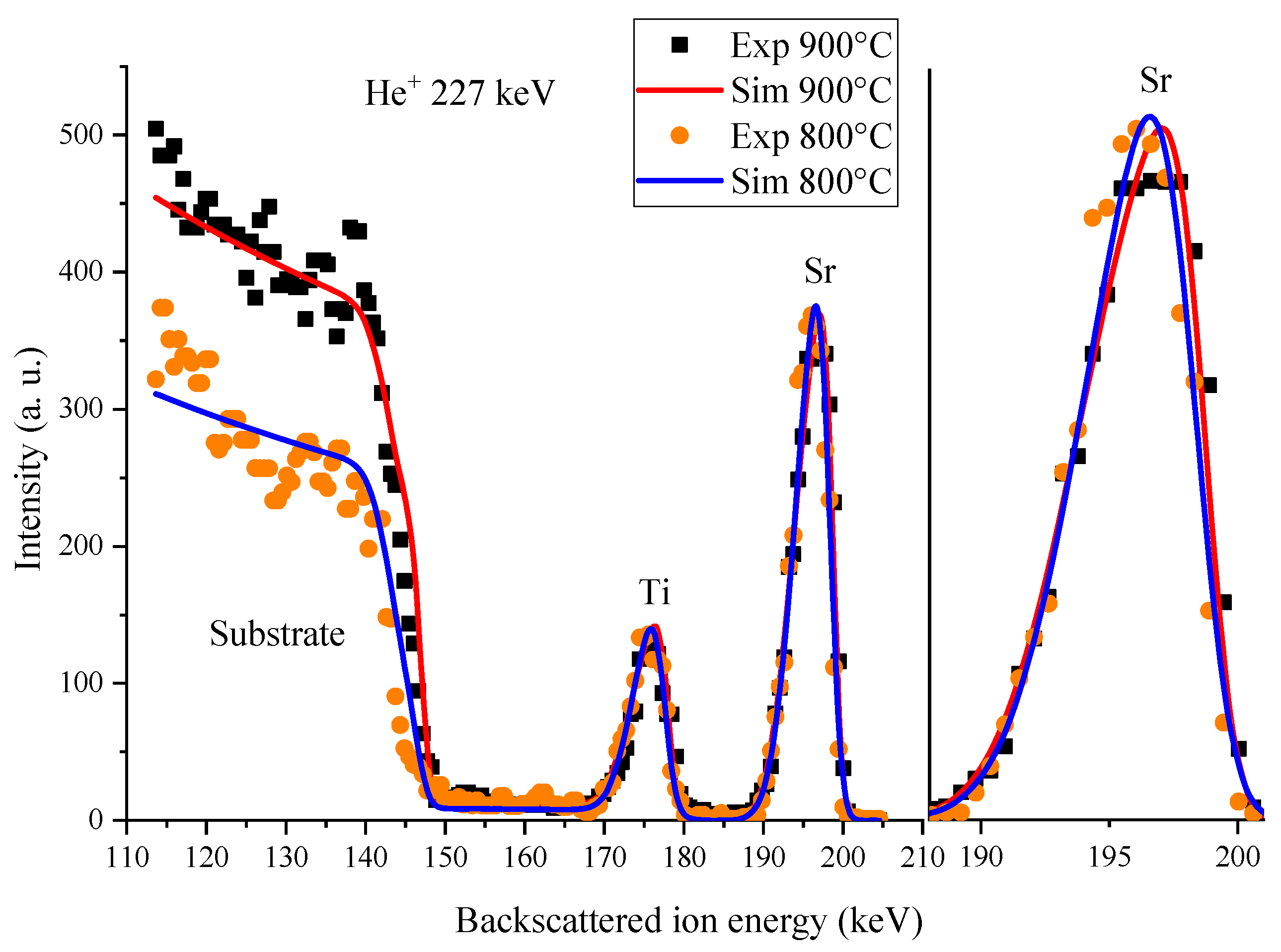
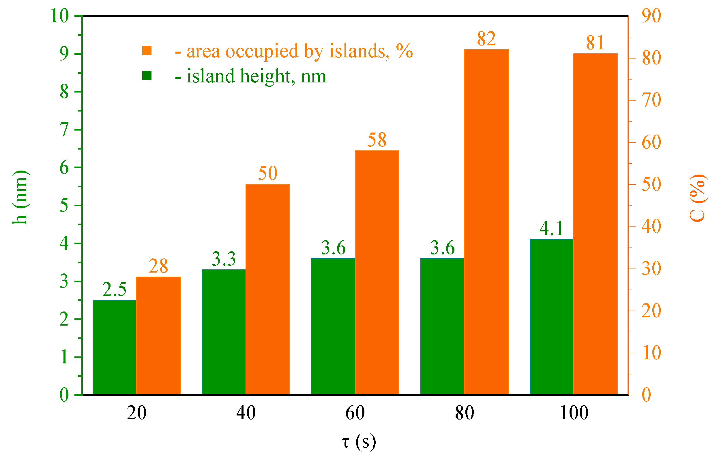
Figure 1. Ion spectra from STO films deposited on an alumina substrate at various temperatures for 60 s.
Coatings 14 00003 g001
Figure 2. The height of the islands and the area of the substrate occupied by the islands, depending on the deposition time of the STO film.
Coatings 14 00003 g002
Figure 3. Diffractograms of thin STO films deposited on an alumina substrate at different substrate temperatures; # represents peaks from the substrate.
Coatings 14 00003 g003
Figure 4. Diffractograms of thin STO film deposited on an alumina substrate at Ts = 900 °C, and subjected to annealing at Tan = 1000 °C; # represents peaks from the substrate.
Coatings 14 00003 g004
Figure 5. Relative content of crystalline phases in STO films deposited at different temperatures.
Coatings 14 00003 g005
Figure 6. Dependence of the capacitance of planar STO capacitors on the control field strength.
Coatings 14 00003 g006
Figure 7. Dependence of the loss tangent of planar STO capacitors on the control field strength.
Coatings 14 00003 g007
Table 1. Comparative characteristics of STO island films investigated. Here τ is the deposition time, h is the height of the islands, σ is the spread of heights, σ/h is the ratio of the spread of heights to the height of the islands, C is the area of the substrate covered by the film, and M is the total amount of substance on the substrate.
SampleSubstrateTs (°C)τ (s)h (nm)σ (nm)σ/hC (%)M
B-379aalumina800202.51.40.56285.1
B-380aalumina800403.32.00.65012.2
B-378aalumina800603.61.60.435815.4
B-381aalumina800803.61.60.438221.7
B-398aalumina8001004.11.60.398124.5
Table 2. Comparative data on the tunability, losses, and CQF of capacitors based on STO films. Here f is the frequency of the measurement, n is the tunability, tanδ (U0) is the loss tangent at zero control voltage, tanδ (Umax) is the loss tangent at maximum applied control voltage, and CQF is the commutation quality factor.
SubstrateDesignf (GHz)n (%)tanδ (U0)tanδ (Umax)CQFRef.
DyScO3planar10570.0470.045360[37]
LaNiO3MDM0.1230.0110.024245[28]
Pt/MgOMDM0.0001710.020.0155949[33]
Pt/Sapphire4 electrode30530.0410.022690[34]
Pt/Sapphire4 electrode10410.0150.0111730[29]
Pt/SapphireMDM5.6430.10.027120[27]
Pt/SapphireMDM1.5500.0160.0211490[45]
DyScO3planar10500.0710.06120[46]
DyScO3planar10660.190.1161[47]
Pt/SapphireMDM1.5600.0140.0213000[48]
Aluminaplanar2460.0090.0143100This work
Disclaimer/Publisher’s Note: The statements, opinions and data contained in all publications are solely those of the individual author(s) and contributor(s) and not of MDPI and/or the editor(s). MDPI and/or the editor(s) disclaim responsibility for any injury to people or property resulting from any ideas, methods, instructions or products referred to in the content.

