Article

Development and Characterization of an Advanced Voltage-Controllable Capacitor Based on AlInGaN/GaN-Si (111) Epitaxy

School of Microelectronics, Northwestern Polytechnical University, Xi’an 710072, China
*
Author to whom correspondence should be addressed.
Coatings 2024, 14(10), 1254; https://doi.org/10.3390/coatings14101254 (registering DOI)
Submission received: 27 August 2024 / Revised: 19 September 2024 / Accepted: 25 September 2024 / Published: 1 October 2024

Abstract

:
The AlInGaN/GaN heterojunction epitaxy material with high cutoff frequency and saturated power density has become a very popular candidate for millimeter wave applications in next-generation mobile communication. In this study, an advanced voltage-controllable capacitor based on the AlInGaN/GaN-Si (111) epitaxy was proposed by employing a bi-directional series MIS capacitor structure. The capacitor was fabricated by using a pad area of 40 μm × 40 μm, with a 1 μm distance between the positive and negative electrodes. The test results show that the capacitance is turned on with a saturation capacitance density and a maximum leakage current density of 0.30 fF/μm2 of 0.37 pA/μm2, respectively, for the control voltage from −6.5 V to 6 V. In particular, in the proposed design method, the saturation capacitance required for the practical application can be obtained by simply adjusting the capacitance area. The capacitor showcases characteristics of rapid turn-on and turn-off responses coupled with low loss, underscoring its promising prospects for deployment in RF switching applications.

1. Introduction

Gallium nitride (GaN) has been widely applied in the field of radiofrequency (RF) mobile communication due to its superior physical properties, such as a large bandgap, optimal thermal conductivity, etc. Therefore, GaN is considered the most promising technology for intergradation of the RF front-end module for RF mobile communication [1,2,3].
Compared to the traditional AlGaN/GaN heterojunction epitaxy, which is predominantly employed in the RF field within the sub-6 GHz frequency band [4,5,6,7,8,9,10], the new AlInGaN/GaN heterojunction epitaxy material, characterized by its higher cutoff frequency and saturated power density, emerges as a promising contender for millimeter wave applications in next-generation mobile communication [11,12]. In particular, the development of the integrated AlInGaN/GaN process on a Si substrate instead of a SiC substrate is expected to benefit from cost effectiveness
Currently, various traditional devices based on AlInGaN/GaN heterojunction epitaxy, including High Electron Mobility Transistors (HEMTs), have been successfully demonstrated [13,14,15,16]. To expand the application range of AlInGaN/GaN heterojunction epitaxy, the development of novel devices is essential. In this study, we propose an innovative device design methodology for a voltage-controllable capacitor utilizing a bi-directional series Metal–Insulator–Semiconductor (MIS) structure, which represents a novel design approach for precision voltage control and dynamic capacitance modulation. This capacitor, fabricated using a pad area of 40 µm × 40 µm with a 1 µm electrode spacing, demonstrates remarkable performance characteristics by leveraging the superior properties of the advanced epitaxy material, AlInGaN/GaN heterojunction epitaxy. The test results reveal that the capacitance can be effectively tuned with a saturation capacitance density of 0.30 fF/µm2 and a maximum leakage current density of 0.37 pA/µm2 within a control voltage range of –6.5 V to 6 V. Notably, the proposed design offers the scalability and flexibility to achieve the desired saturation capacitance simply by adjusting the capacitance area, a feature that is highly desirable for practical applications. Moreover, the capacitor exhibits low loss and reliable turn-on/off characteristics, positioning it as a promising candidate for RF switch applications and advanced electronic systems requiring precise signal manipulation and minimal energy losses. The successful fabrication and characterization of this voltage-controllable capacitor based on AlInGaN/GaN-Si (111) epitaxy represent a significant step forward in the development of advanced RF devices for 5G and future communication systems.

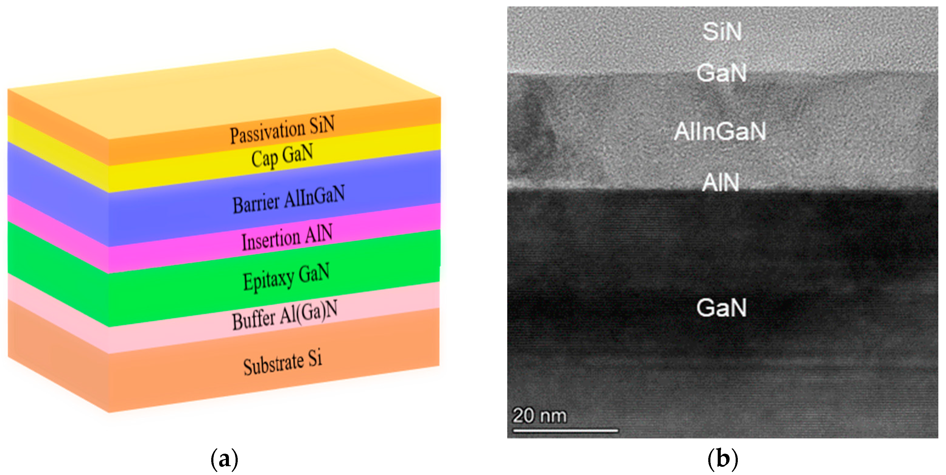
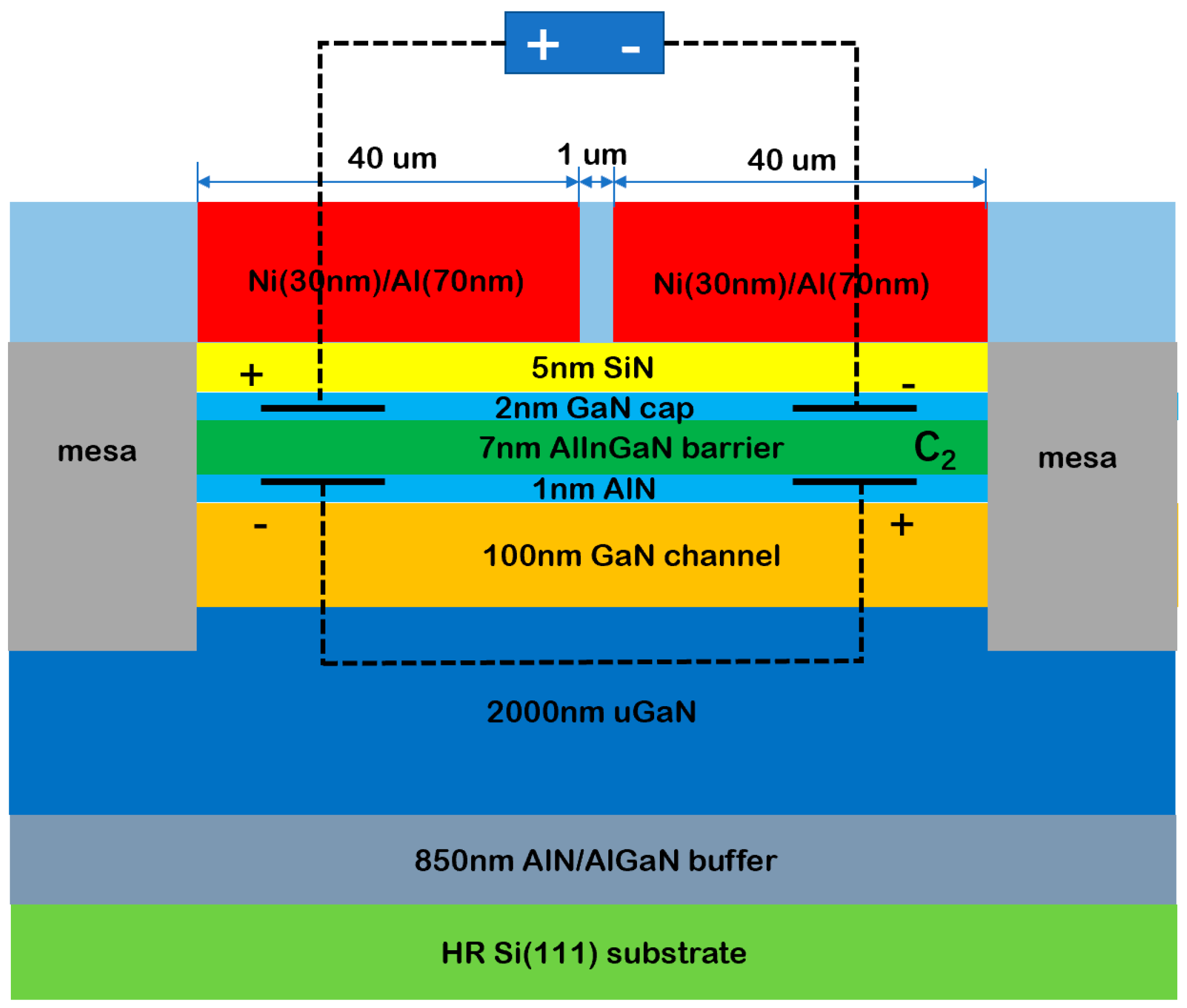
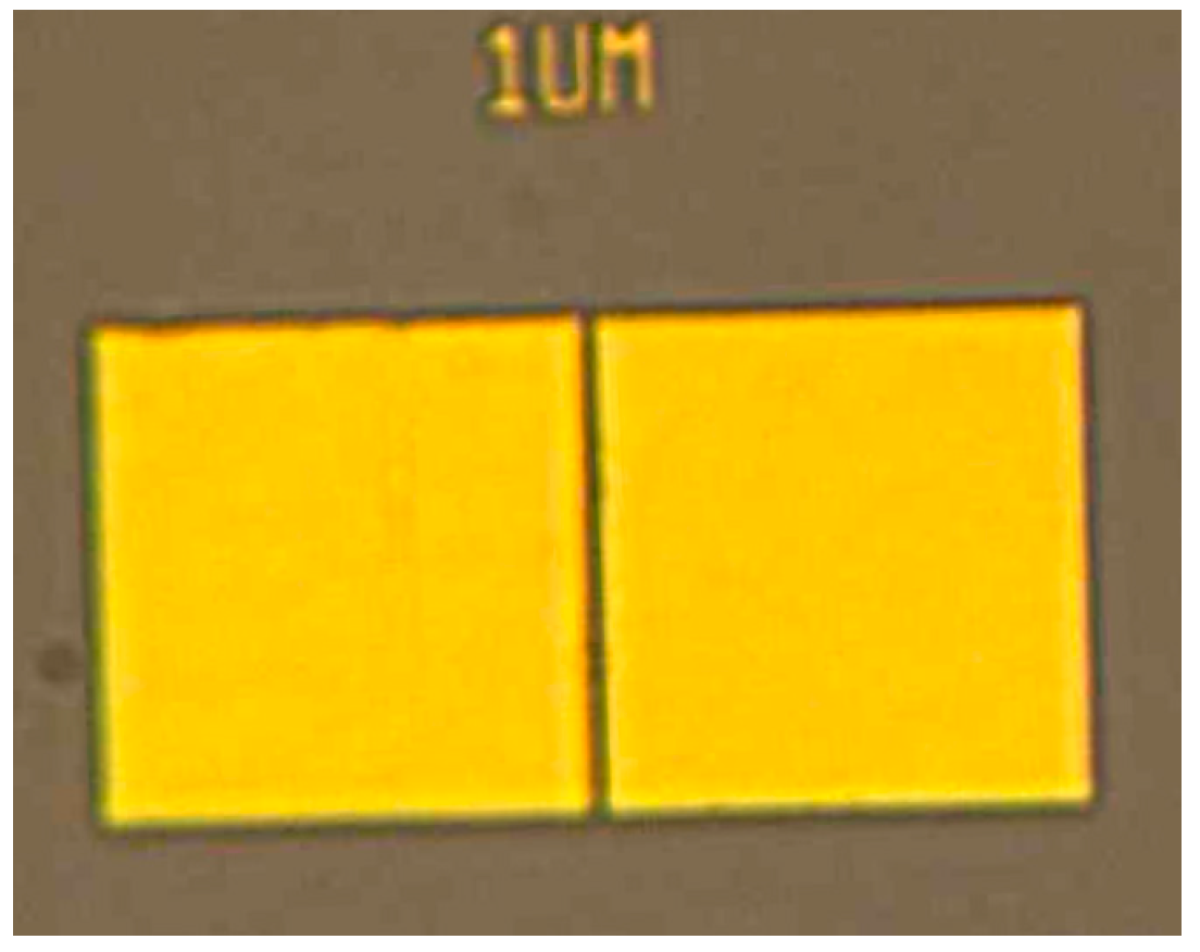
2. Device Design and Manufacture

The epitaxy was grown by employing the metal–organic chemical vapor deposition (MOCVD). As shown in Figure 1a, the epitaxy structure and process have been reported in our previous paper in Ref. [17] as following: High-resistance Si (111) with thickness of 1 × 10⁶ nm was chosen as the substrate for the RF application. An external layer of AlN/AlGaN was deposited on the Si substrate as the buffer layer, and the Al component gradually decreases from bottom to top to reduce the crystal and thermal mismatch between the Si substrate and GaN material, shown in Figure 1d. A 2000 nm uGaN epitaxial layer was grown on the surface of the buffer layer; a 150 nm GaN layer was grown on the buffer to be the channel; a 1 nm thick AlN insertion layer was grown on the GaN channel to improve the two-dimensional gas (2 DEG) of the device; a 7 nm thick undoped InAlGaN barrier layer with Al composition of 45% was grown to be the barrier; and a 2 nm thick GaN cap layer was grown on the surface of the barrier layer as the protective layer. Finally, a thin SiN isolator layer with a thickness of 5 nm was deposited on the surface of epitaxy by using the LPCVD method. The TEM (transmission electron microscope) characterization of the sample is shown in Figure 1b,c, which show clear interfaces and good epitaxial quality. The mobility, carrier density, and square resistance (Rs) of the epitaxy sample are observed by Hall test to be 2894.24 cm2/V·S, 1.930×1013 cm−2, and 170.6 Ω/sq, respectively [17]. The values are observed to be much higher than the traditional AlGaN/GaN-Si (111) epitaxies for RF applications [4,18,19], and demonstrate a comparable 2 DEG mobility and sheet resistance to those grown on SiC [12,13,20]. The excellent electrical performance test results show that the epitaxy designed in this paper has a broad application prospect in the field of high-frequency microwaves, and can realize the large-size epitaxial preparation based on Si substrate to reduce the cost.
A bi-directional series MIS structure was employed to develop the voltage control capacitor. The schematic of the device structure is shown in Figure 2. This structure comprises the two MIS capacitors with opposite polarity connected in series. The distance between the positive and negative electrodes is kept at 1 μm, whereas the areas of the two pads (S) are designed to be 40 μm × 40 μm. As the two capacitors have the same area, the total equivalent capacitance of the device is calculated as εS/2πkd, where d is the thickness of SiN, k is the Boltzmann constant, and ε is the constant of SiN. It is noted that the capacitance of the device is directly proportional to the electrode area; thus, different capacitance values can be obtained by adjusting the area of the pads. This design approach offers significant flexibility, enabling the creation of capacitors with tailored capacitance ranges to suit a wide array of applications. By leveraging the inherent advantages of the MIS structure, including its high breakdown voltage, low leakage current, and excellent frequency response, this bi-directional series MIS capacitor stands as a promising candidate for use in advanced electronic systems requiring precise voltage control and dynamic capacitance modulation.
The fabrication process of the capacitor includes the Mesa isolation and metal electrode growth. The first step of the process is the Mesa isolation in order to realize the electrical isolation of the active region. This step includes two parts: UV photolithography and ion implantation. For photolithography, a 6130 photoresist with a thickness of 3 μm was chosen. Subsequently, the samples were photoetched in MA6 and developed with 3038 for 45 s. Finally, the samples were washed using DI water and dried with a N2 gun. Ion implantation was carried out by using F plasma with 25 keV and 2 × 1014 cm2. Secondly, metal electrode growth included the electron beam lithography (EBL) and metal deposition. The EBL was carried out by using the following procedure: PMMA A4 with a thickness of ~200 nm was used as the photoresist. Subsequently, an EBL exposure was carried by NB5, immediately followed by the precise development of the sample using a specialized developer solution. To complete the fixation process, isopropyl alcohol (IPA) was chosen to delicately treat the sample. Finally, the metal deposition was carried out in the following way: Ni (30 nm)/Au (70 nm) was deposited using an electron-beam metal evaporator. Subsequently, the samples were immersed in acetone for 2 h and isopropanol solution for 5 min to complete the metal stripping. Afterwards, the samples were blow dried with N2. Finally, an O2 plasma treatment was employed to remove the residual photoresist. The optical microscopy image of the device is shown in Figure 3.

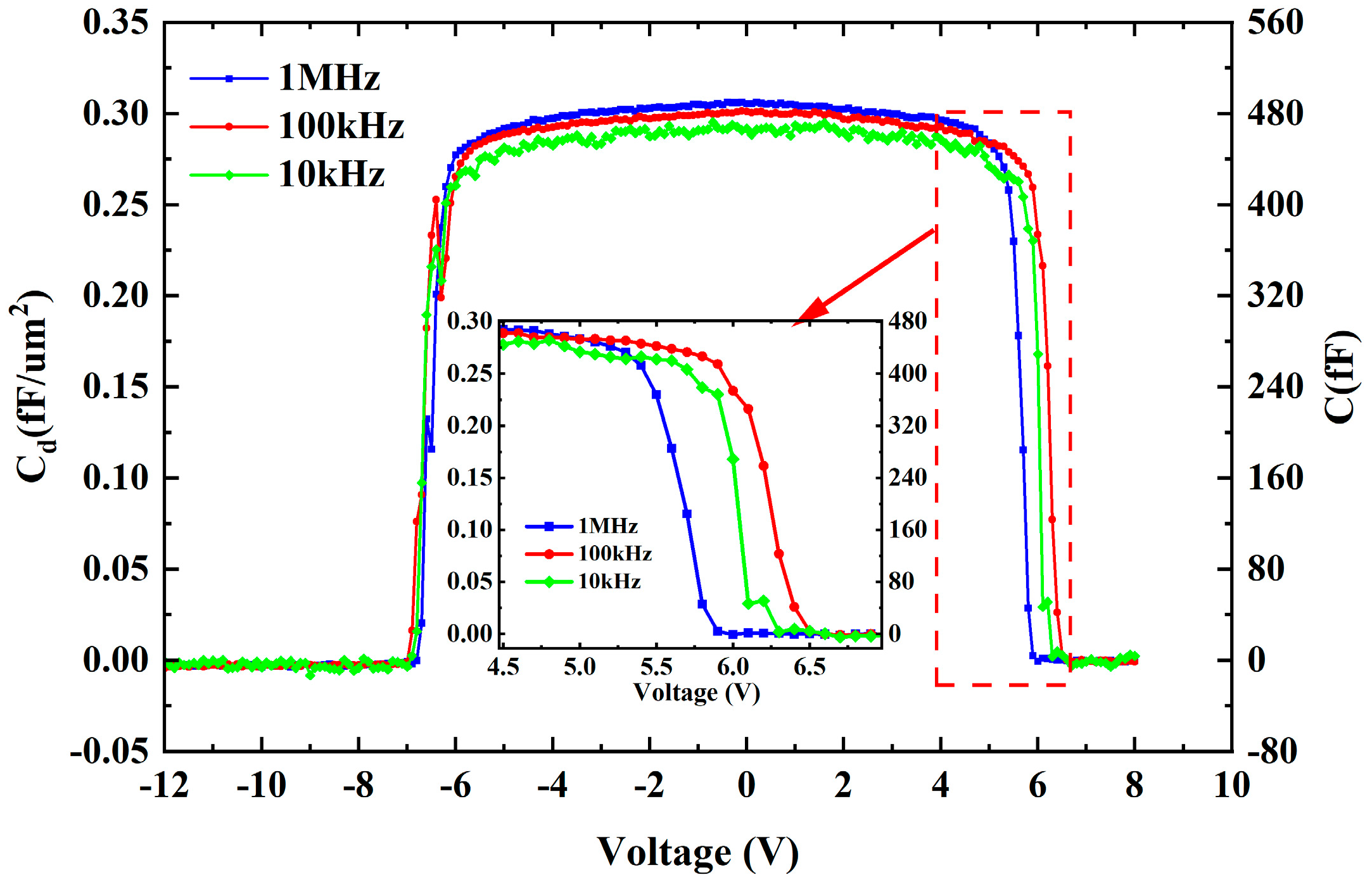
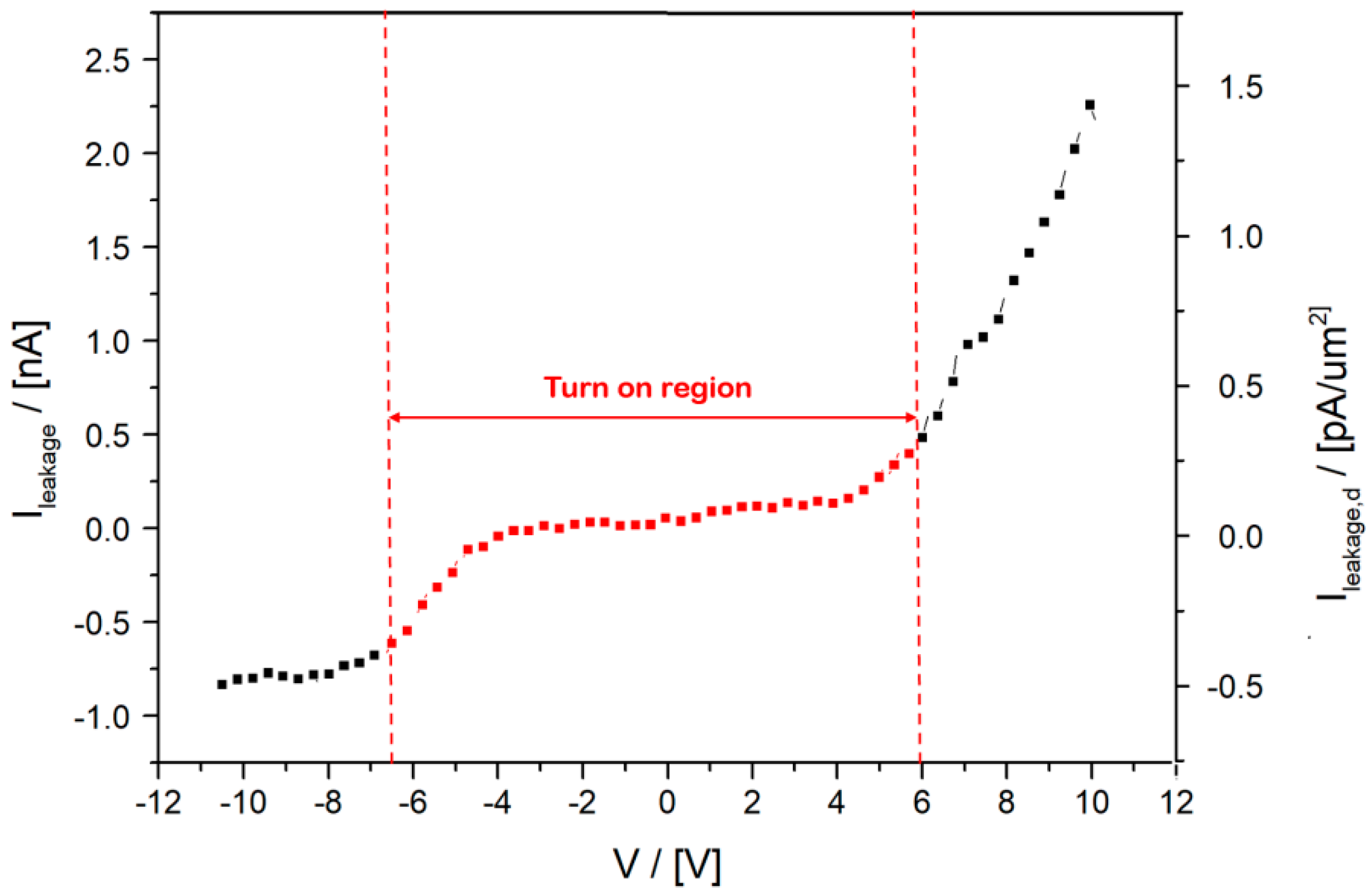
3. Test and Discussion

The device was subjected to the C-V test. During the test, the voltage (V) was swept from −10 V to 8 V, with incremental steps of 100 mV, allowing for a detailed examination of the device’s behavior. As shown in Figure 4, the capacitance response demonstrated a distinctive turn-on characteristic. The saturation capacitance (Cox) and saturation capacitance density (Cox,d) were observed for control voltages ranging from −6.5 V to 6 V, indicating robust performance across a wide voltage range. The Cox and Cox,d values at 10 kHz were approximately 430 fF and 0.27 fF/µm2, respectively. For the 100 kHz frequency, a Cox of approximately 440 fF and a corresponding Cox,d of roughly 0.28 fF/μm2 were observed. This saturation point was observed for control voltages ranging from −6.5 V to 6 V, indicating robust performance across a wide voltage range. A high opening speed is inferred from the sharp turn-on characteristics observed in the C-V test curves (Figure 4), which demonstrate a rapid transition from the off-state to the on-state within a narrow voltage range, and vice versa. The high opening speed of the capacitor, a testament to its swift response to voltage changes, can be attributed to the exceptional interfacial properties between the InAlGaN/GaN-Si heterojunction material, the SiN passivation layer, and the good ohmic contact process. These interfaces facilitate efficient charge transfer and minimize resistive losses, resulting in the observed rapid switching behavior. When the test frequency was escalated to 1 MHz, an increase in Cox and Cox,d was observed with values rising to approximately 480 fF and 0.30 fF/μm2, respectively. This frequency-dependent behavior illustrates the dynamic nature of the device’s capacitance; thus, this is a crucial aspect for applications requiring precise control over electrical properties at high frequencies. As discussed above, the saturated capacitance of the device is directly proportional to the electrode area; thus, the electrode area of the capacitor can be adjusted to obtain a suitable capacitance value for different applications. The saturated capacitance of the device is intimately linked to the electrode area. This inherent scalability offers a significant advantage, as the electrode area can be tailored to suit specific application requirements. For instance, larger electrode areas can be employed to achieve higher capacitance values for energy storage or filtering applications, while smaller areas may be preferable for high-speed signal processing or RF switching circuits, where reduced parasitic elements and enhanced performance are paramount.
Furthermore, the capacitor’s performance in terms of leakage current is as illustrated in Figure 5. In the turn-on region, the leakage current (Ileakage) remains exceptionally low at a value of −0.7~0.5 nA, while the maximum leakage current density (Ileakage,d) stands at a mere 0.37 pA/μm2. Such minimal leakage figures are indicative of a device with extremely low power dissipation, promising significant energy savings and heightened efficiency during operational use, compared to traditional AlGaN/GaN HEMT on a Si substrate and AlInGaN HEMT on a SiC substrate [21,22]. This characteristic, coupled with the device’s superior capacitance tunability and high-frequency response, positions it as an attractive candidate for incorporation into sophisticated electronic systems demanding precise voltage control and dynamic capacitance modulation while minimizing energy losses.

4. Conclusions

In this study, an epitaxy sample InAlGaN/GaN based on Si was prepared, and a voltage control switch capacitor with a bi-directional series MIS structure was subsequently proposed and successfully fabricated. The capacitor designed with a pad area of 40 μm × 40 μm and 1 μm distance between the positive and negative electrodes shows a saturation capacitance and saturation capacitance density of ~480 fF and 0.30 fF/μm2, respectively, for the control voltage from −6.5 V to 6 V at 1 MHz, with a fast capacitor switch speed. In particular, in the proposed design method, the saturation capacitance required for practical applications can be obtained by simply adjusting the capacitance area. In addition, the capacitor shows a very low value of the leakage current (−0.7~0.5 nA) and the maximum leakage current density (0.37 pA/μm2) in the turn-on region. Given its notable turn-on/off performance and low loss characteristics, this capacitor holds immense potential for applications in RF switch circuits. Its ability to dynamically modulate capacitance and precisely control voltage, coupled with its low energy consumption, makes it an attractive candidate for incorporation into advanced electronic systems requiring precise signal manipulation and minimal energy losses.

Author Contributions

Conceptualization, methodology, writing—original draft, H.G.; writing—review and editing, G.S. All authors have read and agreed to the published version of the manuscript.

Funding

This research was funded by the “National key R & D plan of China, Grant No. 2023YFB2905200”, “National Natural Science Foundation of China, Grant No. 62471402”, Key R & D plan of Shaanxi province, China, Grant No.2023GXLH-084”, and “Innovation Foundation for Doctor Dissertation of Northwestern Polytechnical University, Grant No. CX2024086”.

Institutional Review Board Statement

Not applicable.

Data Availability Statement

Data is contained within the article.

Conflicts of Interest

The authors declare no conflict of interest.

References

  1. Sun, H.; Marti, D.; Tirelli, S.; Alt, A.R.; Benedickter, H.; Bolognesi, C. Millimeter-wave GaN-based HEMT development at ETH-Zürich. Int. J. Microw. Wirel. Technol. 2010, 2, 33–38. [Google Scholar] [CrossRef]
  2. Mishra, U.K.; Parikh, P.; Wu, Y.F. AlGaN/GaN HEMTs-an overview of device operation and applications. Proc. IEEE 2002, 90, 1022–1031. [Google Scholar] [CrossRef]
  3. Palacios, T.; Chakraborty, A.; Rajan, S.; Poblenz, C.; Keller, S.; DenBaars, S.; Mishra, U. High-power AlGaN/GaN HEMTs for ka-band applications. IEEE Electron Device Lett. 2005, 26, 781–783. [Google Scholar] [CrossRef]
  4. Chung, J.W.; Hoke, W.E.; Chumbes, E.M.; Palacios, T. AlGaN/GaN HEMT with 300-GHz fmax. IEEE Electron Device Lett. 2010, 31, 195–197. [Google Scholar] [CrossRef]
  5. Palacios, T.; Dora, Y.; Chakraborty, A.; Sanabria, C.; Keller, S.; DenBaars, S.P.; Mishra, U.K. Optimization of AlGaN/GaN HEMTs for high frequency operation. Phys. Status Solidi A 2006, 203, 1493. [Google Scholar] [CrossRef]
  6. Higashiwaki, M.; Mimura, T.; Matsui, T. AlGaN/GaN heterostructure field-effect transistors on 4H-SiC substrates with current-gain cutoff frequency of 190 GHz. Appl. Phys. Express 2008, 1, 021103. [Google Scholar] [CrossRef]
  7. Kumar, V.; Lu, W.; Schwindt, R.; Kuliev, A.; Simin, G.; Yang, J.; Khan, M.A.; Adesida, I. AlGaN/GaN HEMTs on SiC with fT of over 120 GHz. IEEE Electron Device Lett. 2002, 23, 455–457. [Google Scholar] [CrossRef]
  8. Christy, P.D.; Katayama, Y.; Wakejima, A.; Egawa, T. High fT and fMAX for 100 nm unpassivated rectangular gate AlGaN/GaN HEMT on high resistive silicon (111) substrate. Electron. Lett. 2015, 51, 1366–1368. [Google Scholar] [CrossRef]
  9. Schwindt, R.; Kumar, V.; Kuliev, A.; Simin, G.; Yang, J.; Khan, M.; Muir, M.; Adesida, I. Millimeter-wave high-power 0.25-μm gate-length AlGaN/GaN HEMTs on SiC substrates. IEEE Microw. Wirel. Compon. Lett. 2003, 13, 93–95. [Google Scholar] [CrossRef]
  10. Dumka, D.; Lee, C.; Tserng, H.; Saunier, P.; Kumar, M. AlGaN/GaN HEMTs on Si substrate with 7 W/mm output power density at 10 GHz. Electron. Lett. 2004, 40, 1023–1024. [Google Scholar] [CrossRef]
  11. Makiyama, K.; Ozaki, S.; Niida, Y. InAlGaN/GaN-HEMT device technologies for W-band high-power amplifier. In Proceedings of the 2016 Lester Eastman Conference (LEC), Bethlehem, PA, USA, 2–4 August 2016; pp. 31–34. [Google Scholar]
  12. Lee, D.S.; Laboutin, O.; Cao, Y.; Johnson, W.; Beam, E.; Ketterson, A.; Schuette, M.; Saunier, P.; Kopp, D.; Fay, P.; et al. 317 GHz InAlGaN/GaN HEMTs with extremely low on-resistance. Phys. Status Solidi C 2013, 10, 827–830. [Google Scholar] [CrossRef]
  13. Tsai, P.; Nguyen, H.; Nagarajan, V.; Lin, C.; Dee, C.; Chen, S.; Kuo, H.; Lee, C.; Chang, E.Y. Enhancement-Mode High-Frequency InAlGaN/GaN MIS-HEMT Fabricated by Implementing Oxygen-Based Digital Etching on the Quaternary Layer. ECS J. Solid State Sci. Technol. 2022, 11, 085005. [Google Scholar] [CrossRef]
  14. Mukherjee, H.; Kar, M.; Kundu, A.J. Enhancement in Analog/RF and Power Performance of Underlapped Dual-Gate GaN-Based MOSHEMTs with Quaternary InAlGaN Barrier of Varying Widths. Electron. Mater. 2022, 51, 692–703. [Google Scholar] [CrossRef]
  15. Yaita, J.; Yamada, A.; Nakamura, N.; Kotani, J. Probing the effects of surface roughness and barrier layer thickness in InAlGaN/GaN HEMTs to improve carrier mobility. Appl. Phys. Express 2021, 14, 031005. [Google Scholar] [CrossRef]
  16. Sanyal, I.; Lin, E.S.; Wan, Y.C.; Chen, K.M.; Tu, P.T.; Yeh, P.C.; Chyi, J.I. AlInGaN/GaN HEMTs with high Johnson’s figure-of-merit on low resistivity silicon substrate. IEEE J. Electron Devices Soc. 2021, 9, 130–136. [Google Scholar] [CrossRef]
  17. Guan, H.; He, L.; Wu, J.; Zeng, Z.; Li, Y.; Deng, B.; Shen, G.; Li, W.; Wang, Y. Fabrication and Characterization of a Novel Varistor Based on AlInGaN/GaN Heterojunction Epitaxy on High Resistance Silicon (111) Substrates. IEEE Trans. Electron Devices 2022, 69, 4200–4205. [Google Scholar] [CrossRef]
  18. Lecourt, F.; Douvry, Y.; Defrance, N.; Hoel, V.; De Jaeger, J.; Bouzid, S.; Renvoise, M.; Smith, D.; Maher, H. High transconductance AlGaN/GaN HEMT with thin barrier on Si (111) substrate. In Proceedings of the European Solid-State Device Research Conference (ESSDERC), Sevilla, Spain, 14–16 September 2010; pp. 281–284. [Google Scholar]
  19. Aubry, R.; Jacquet, J.C.; Oualli, M. ICP-CVD SiN passivation for high-power RF InAlGaN/GaN/SiC HEMT. IEEE Electron Device Lett. 2016, 37, 629–632. [Google Scholar] [CrossRef]
  20. Yamada, A.; Minoura, Y.; Kurahashi, N.; Kamada, Y.; Ohki, T.; Sato, M.; Nakamura, N. 31 W/mm at 8 GHz in InAlGaN/GaN HEMT with thermal CVD SiNx passivation. IEEE Electron Device Lett. 2024, 45, 324–327. [Google Scholar] [CrossRef]
  21. Guan, H.; Shen, G.; Gao, B.; Zhang, H.; Wang, Y.; Wang, S. A study on the optimized ohmic contact process of AlGaN/GaN-Si MIS-HEMTs. IEEE Access 2021, 9, 9855–9863. [Google Scholar] [CrossRef]
  22. Zhu, G.; Kong, Y.; Zhang, K.; Yu, X.; Chen, T. InAlGaN ultra-thin barrier layer structure high frequency GaN HEMT device. Res. Prog. Solid State Electron. 2017, 37, 299–302. [Google Scholar]
Figure 1. The InAlGaN/GaN-Si epitaxy schematic and test result; (a) is the schematic of the AlInGaN/GaN epitaxy structure, (b) is the TEM analysis of AlInGaN/GaN heterojunction, (c) is the TEM analysis of AlN/AlGaN buffer layer, and (d) is the EDS Scan result of Al.
Coatings 14 01254 g001aCoatings 14 01254 g001b
Figure 2. The schematic of the device structure and the equivalent circuit of the device.
Coatings 14 01254 g002
Figure 3. The optical microscopy.
Coatings 14 01254 g003
Figure 4. The C-V test curves of the capacitor.
Coatings 14 01254 g004
Figure 5. The I-V test curves of the capacitor.
Coatings 14 01254 g005
Disclaimer/Publisher’s Note: The statements, opinions and data contained in all publications are solely those of the individual author(s) and contributor(s) and not of MDPI and/or the editor(s). MDPI and/or the editor(s) disclaim responsibility for any injury to people or property resulting from any ideas, methods, instructions or products referred to in the content.

