Article

The Impact of Thermal Treatment on the Structural, Optical and Electrochemical Characteristics of Tin Sulfide Films

1
Department of Physical and Inorganic Chemistry, Kaunas University of Technology, Radvilenu str. 19, LT-50254 Kaunas, Lithuania
2
NanoTechnas—Center of Nanotechnology and Materials Science, Faculty of Chemistry and Geosciences, Vilnius University, Naugarduko St. 24, LT-03225 Vilnius, Lithuania
3
Department of Organic Chemistry and Technology, Faculty of Chemical Technology and Biotechnology, Budapest University of Technology and Economics, Műegyetem rkp. 3., H-1111 Budapest, Hungary
4
J. Heyrovsky Institute of Physical Chemistry of the AS CR, v.v.i., Dolejskova 2155/3, 182 23 Prague, Czech Republic
*
Author to whom correspondence should be addressed.
Coatings 2024, 14(10), 1284; https://doi.org/10.3390/coatings14101284
Submission received: 18 August 2024 / Revised: 20 September 2024 / Accepted: 29 September 2024 / Published: 8 October 2024
(This article belongs to the Special Issue Optical Coatings: From Materials to Applications)

Abstract

:
The development of eco-friendly, cost-effective, and naturally abundant electrode materials for supercapacitors is gaining critical importance in current energy storage research. This study focuses on the synthesis of tin sulfide (SnSx) films via the eco-friendly successive ionic layer adsorption and reaction (SILAR) method, employing varying quantities of L-ascorbic acid (0.8 and 1.0 g) as a reducing agent. Tin sulfide films were deposited on fluorine-doped tin oxide (FTO) glass substrates and subsequently annealed in an inert atmosphere at temperatures ranging from 200 to 400 °C, resulting in thin films of varying thicknesses (100–420 nm). The structural and compositional characteristics of the films were thoroughly analyzed using Raman spectroscopy to confirm the purity and spectroscopic signatures of the sulfides. Further characterization was performed to assess the films’ morphology (scanning electron microscopy, SEM), phase composition (X-ray diffraction, XRD), surface chemical states (X-ray photoelectron spectroscopy, XPS), optical properties (UV–Vis spectroscopy), and electrical properties (Hall measurements). The gathered data were then used to evaluate the potential of tin sulfide films as electrode materials in supercapacitors, highlighting their suitability for sustainable energy storage applications.

1. Introduction

Energy is a critical factor in global development, with approximately 65% of the world’s energy demand currently met by non-renewable fossil fuels [1]. This reliance contributes to greenhouse gas emissions, global warming, and environmental degradation [2]. To mitigate these issues and address the depletion of fossil fuels, a shift toward renewable energy sources is imperative [3]. In addition to the development of renewable energy, advances in energy storage technologies, particularly electrochemical devices, are essential for efficient energy conversion and storage [4].
Supercapacitors (SCs) have emerged as promising energy storage devices due to their high power density, extended life cycle, and superior energy density compared to traditional capacitors [5]. They are suitable for various electrical and electronic applications [6]. SCs are categorized into electric double-layer capacitors (EDLCs) and pseudocapacitors based on their charge storage mechanisms [7]. Pseudocapacitors, which include materials like metal oxides, metal sulfides, and conductive polymers, generally offer higher capacitance than EDLCs but with a shorter life cycle [8].
Among pseudocapacitive materials, metal chalcogenides, particularly tin sulfides, have garnered significant attention due to their advantageous physicochemical properties [9,10]. Tin-based chalcogenides such as SnS and SnS2 are of particular interest, although research on Sn2S3 remains limited [11]. Tin and sulfur are non-toxic and abundant elements, making tin chalcogenides attractive for energy applications due to their robust structure and excellent electrical and optical properties [12].
SnS, with its orthorhombic structure and a bandgap of approximately 1.1 eV, is comparable to silicon [13] and exhibits promising characteristics for near-infrared applications [14]. SnS2, an n-type semiconductor, adopts a hexagonal structure, while SnS can exhibit both n-type and p-type conductivity, influenced by annealing temperature [15,16]. The properties of these materials make them suitable for a range of applications, including photovoltaic devices [17], supercapacitors [18], optical sensors, and transistors [19].
The synthesis of high-quality thin films using cost-effective and abundant materials remains a challenge. Various deposition methods, such as thermal evaporation [20], chemical bath deposition [21], and spin coating [22], have been explored for tin sulfide films, with photovoltaic applications being the primary motivation [23]. It is well established that post-deposition annealing improves the crystalline quality of tin sulfide films, with optimal results often achieved at temperatures between 300 °C and 600 °C, depending on the desired material properties [14,23,24,25].
Mixed tin sulfides (SnSx) have shown versatility in various technological applications. The successive ionic layer adsorption and reaction (SILAR) method is a cost-effective and efficient approach for thin-film deposition, enabling large-area applications with strong substrate adhesion. This study examined the structural, morphological, optical, and electrical properties of tin sulfide films deposited on FTO glass and annealed in a nitrogen atmosphere at 200–400 °C, highlighting the occurrence of “chemical epitaxy” due to the well-defined orientation of tin sulfide on the substrate [26,27].

2. Materials and Methods

2.1. Materials

As substrates for the deposition of thin films, fluorine-doped tin oxide (FTO) glass slides with a parameters of size of 20 mm × 15 mm and a sheet resistance of 9.38 ± 0.38 Ω/sq were provided by Ossila.com. Labochema. lt served tin chloride dihydrate with a purity of 98%. 98% sodium sulfide nonahydrate was brought by Honeywell.com (Charlotte, NC, USA). The 99% pure form of L-ascorbic acid was purchased from Sigma-Aldrich (Taufkirchen, Germany).

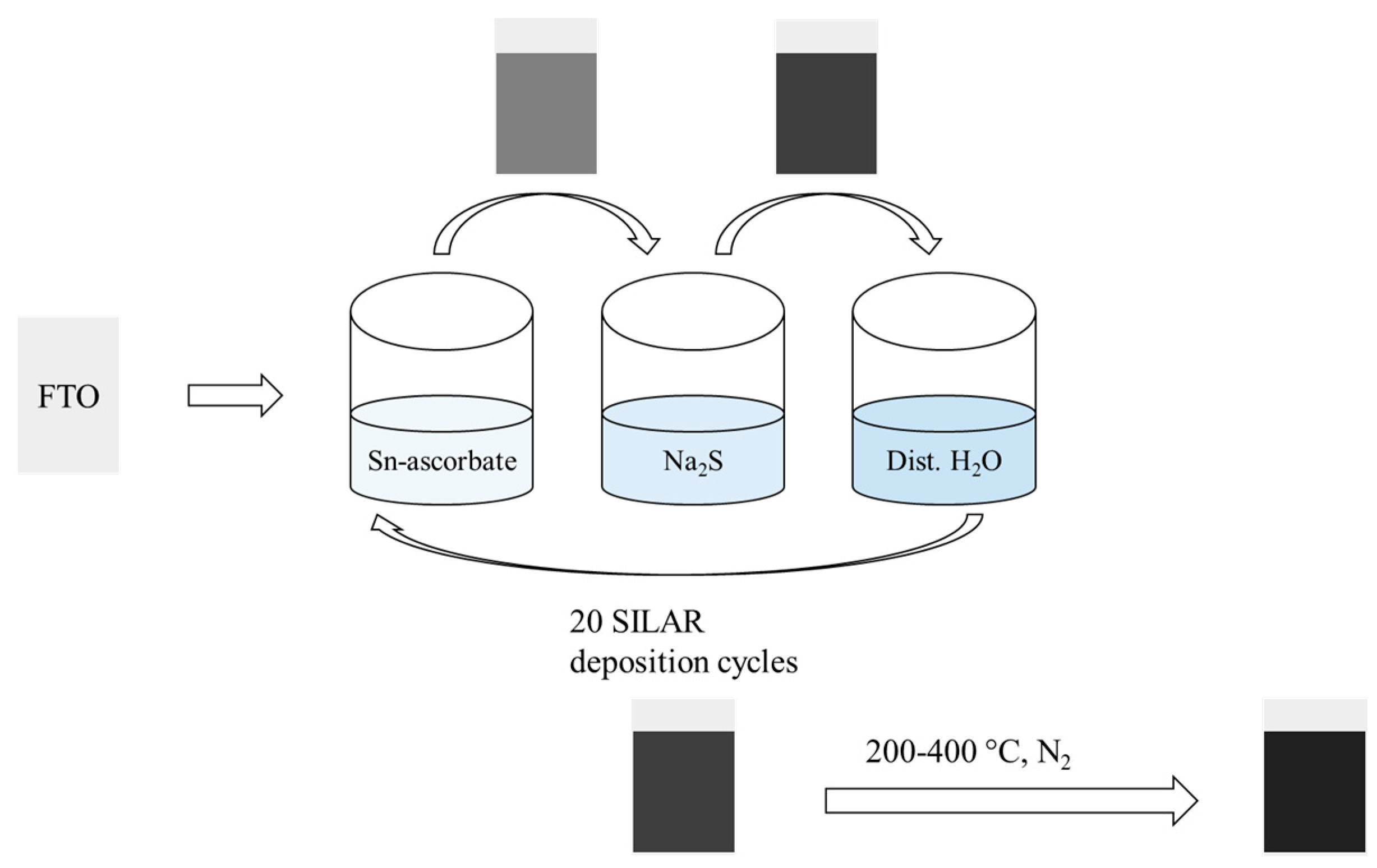
2.2. Film Deposition

For the deposition of a thin tin sulfide film, the SILAR method reported earlier [9] was used. Firstly, the washed FTO glass slides were ultrasonically cleaned in acetone for 10 min. The SILAR method is based on the one-by-one placement of cation and anion precursor solutions and distilled water. The aqueous cationic solution consisted of 0.04 M SnCl2 with 0.8 g or 1.0 g of L-ascorbic acid, and the aqueous anionic solution was 0.04 M Na2S. For the synthesis, 20 SILAR cycles at 40 °C were used. The synthesis mechanism is shown in Scheme 1.
To modify the deposited films, annealing in an inert atmosphere at different temperatures (200 °C, 250 °C, 300 °C, 350 °C, and 400 °C) was applied. The deposition parameters and sample numbers are listed in Table 1.

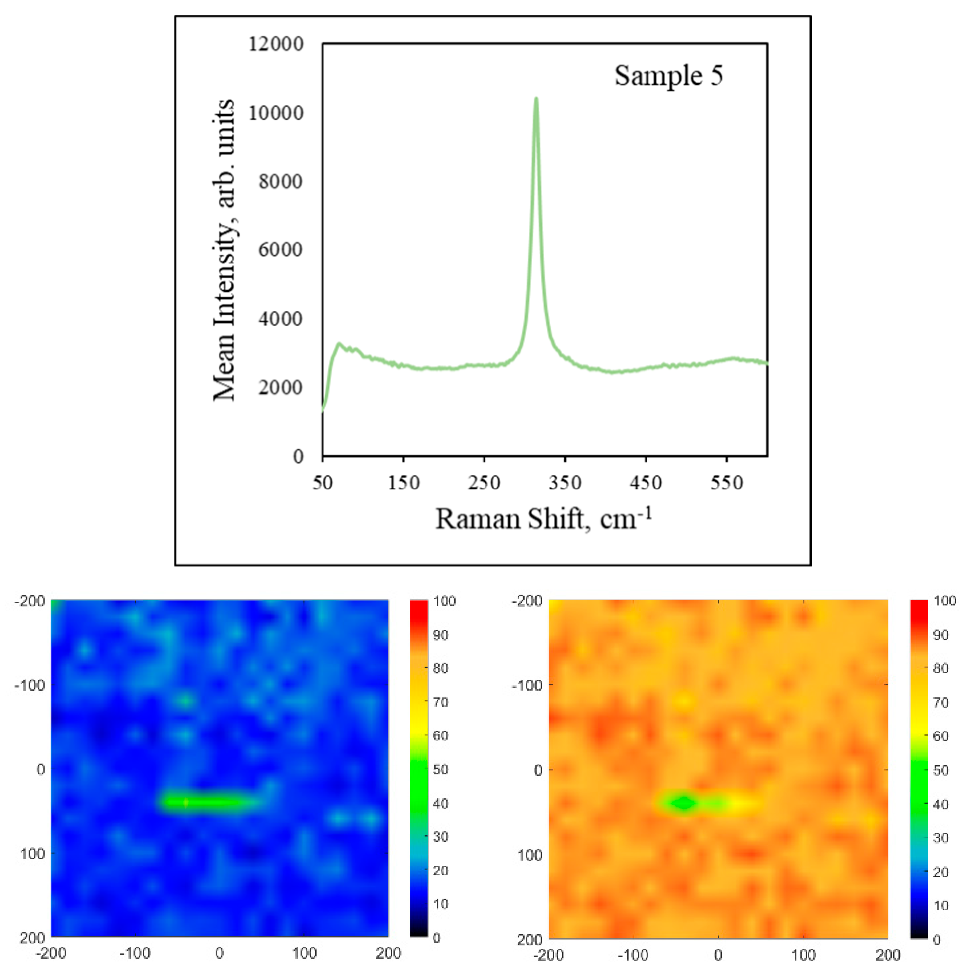
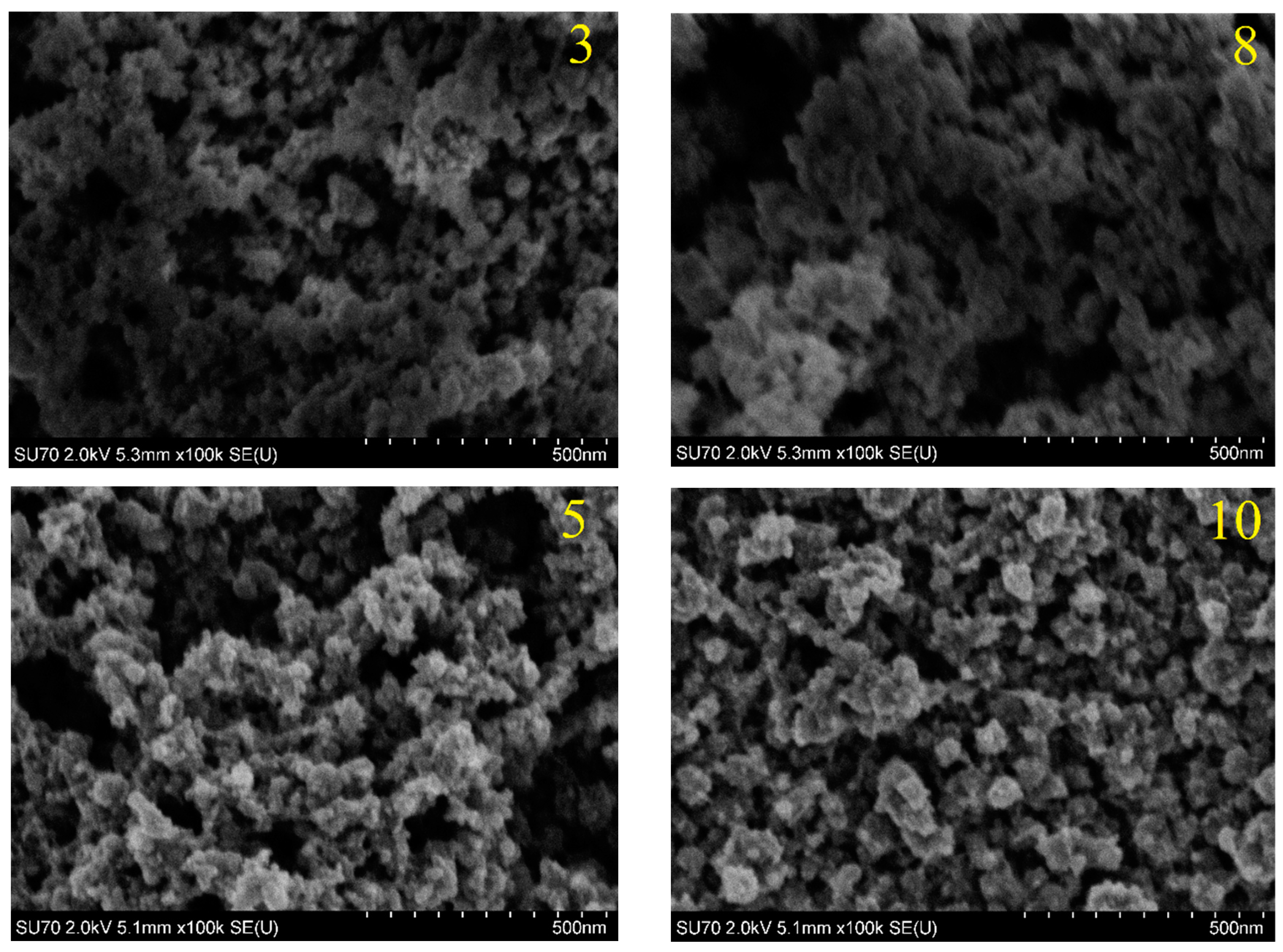
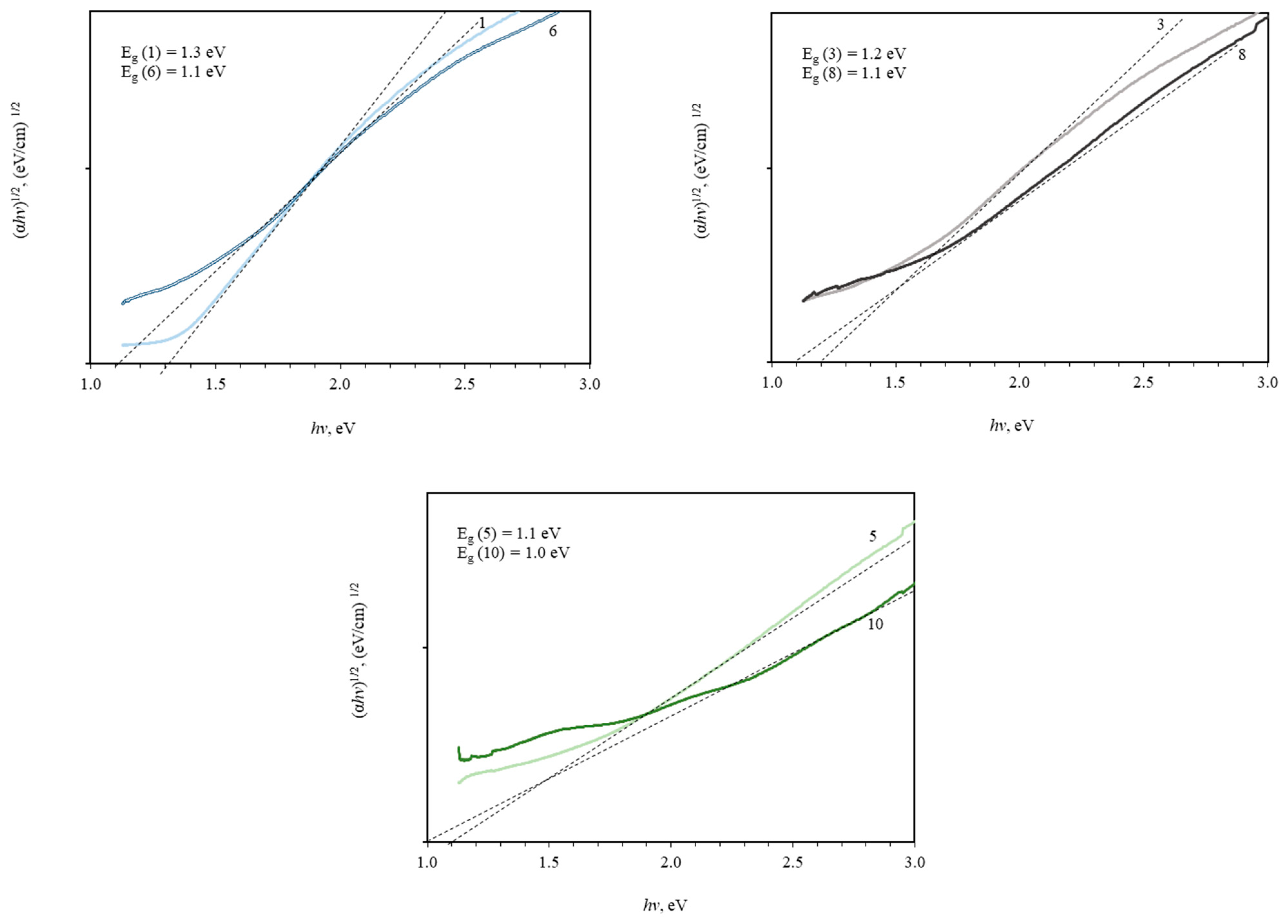
2.3. Characterization of Films
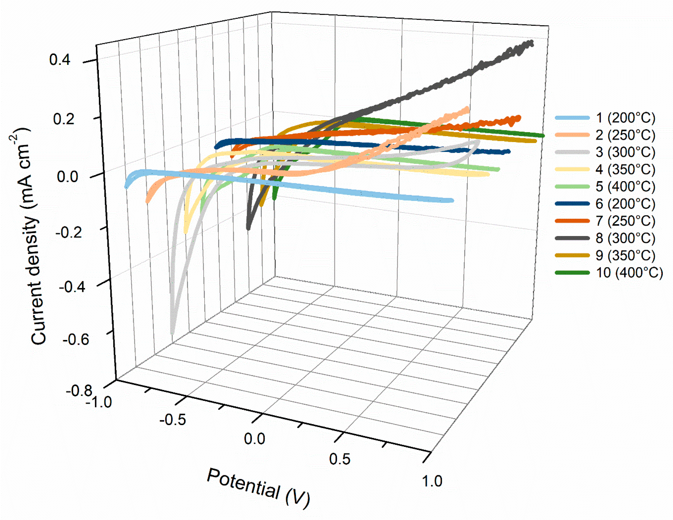
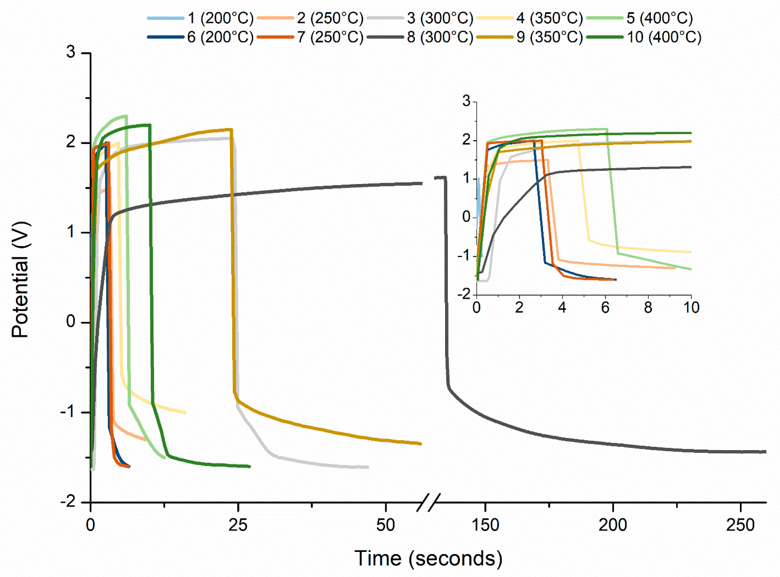
Thin tin sulfide films were characterized using XRD, Raman, SEM, and XPS measurements. UV–Vis spectroscopy and electrochemical calculations were performed on the samples. A description of the methods used is provided in the Supplementary Data.

3. Results

Tin sulfide nanoparticles were synthesized by changing the mass of the capping agent (L-ascorbic acid) via the SILAR route, as shown in Scheme 1. To improve crystallinity, the samples were annealed in an inert atmosphere in the temperature range of 200–400 °C. As-deposited and annealed tin sulfide thin films adhere strongly to the substrate. Furthermore, it was noted that with an increase in the annealing temperature, the obtained films became smoother and thinner.
This section may be divided into subheadings. A concise and precise description of the experimental results, their interpretation, and the conclusions that can be drawn should be provided.
X-ray diffraction. X-ray diffraction (XRD) analysis was utilized to examine the crystalline structure and phase purity of the thin films. The XRD data of the as-prepared tin sulfide films deposited previously under the same conditions [1] agree with the typically reported structure of herzenbergite (ICDD PDF No. 39-0354). Meanwhile, the XRD curves (Figure 1) of Sn-S annealed at different temperatures identify some phase transformations and increased crystallinity. In general, all the annealed films are characterized by the main and most intense peaks at 2θ = 26.64°, 37.88°, and 51.65°, which are assigned to orthorhombic SnS (ICDD PDF No. 83-47). However, SnO2 peaks (ICDD PDF No. 46-1088) can also be identified by these peaks due to the very close values of the interplanar spacing (Table 2). Therefore, other instrumental analysis methods have been used to clarify the prevailing phase of tin sulfide.
Starting at 200 °C, a certain hill at 2θ = 18–35° is barely visible compared to the as-prepared films, which were revealed to be more amorphous [1]. At 250 °C and below, a small peak appears at 2θ = 31.68° (hkl index 310), which is assigned to Sn2S3 (ICDD PDF No. 75-2183). This phase decomposes to SnS2 and SnS at temperatures above 300 °C [2,3] via the following reaction route: Sn2S3 → SnS2 + SnS. A further increase in the annealing temperature highlights the presence of hexagonal SnS2 (mineral berndite, ICDD PDF No. 83-1705) with a small peak at 2θ = 16.00° (hkl index 001). Although the XRD spectra of films annealed at 300 and 350 °C do not disclose any SnS2 peaks, this particular phase shows poor crystallinity and can be intangible by the XRD technique [4,5,6]. Furthermore, due to the desulfurization of SnS2 to SnS and S above 350 °C [4,7], this phase no longer exists in the 400 °C spectrum.
The quantity of L-ascorbic acid was found to not affect the phase composition as the spectra are similar when 0.8 g and 1.0 g are used. However, it appears that a higher amount of ascorbic acid improves the crystallinity of the films because the spectra obtained with 1.0 g are smoother.
In summarizing the results of the XRD analysis, it can be emphasized that the diffraction patterns indicate a mixed-phase composition of the samples, whereas the main peaks are assigned to SnS. The annealing temperature promotes the desulfurization process of the secondary phases, so it is likely that the purest films with a predominant SnS are obtained at a temperature of 400 °C. However, XRD is a one-point analysis technique [8]; therefore, the possibility of the existence of secondary phases (SnS2 and Sn2S3) should not be ignored. To check the reliability of the results, other methods of instrumental analysis, Raman mapping and XPS, have been conducted in this work. Since more pronounced changes in the structure of the films occur approximately every 100 °C, the samples heated at temperatures of 200, 300, and 400 °C were selected for further analysis, eliminating intermediate temperatures.
Crystallite size was determined using the most prominent XRD peaks. Compared to the findings in a previous report [9], annealing resulted in an increase in the crystallite size. When utilizing 0.8 g of L-ascorbic acid, there was a slight variation in particle size, ranging between 33 and 35 nm. Elevated temperatures influenced the crystallite size, leading to a reduction. Conversely, a higher amount (1.0 g) of L-ascorbic acid led to the formation of larger particles. As the annealing temperature increased, the particle size exhibited significant variation within a broader range of 30–35 nm. To generate smaller crystallites of tin sulfide, higher annealing temperatures and reduced quantities of L-ascorbic acid are required.
Raman studies. The Raman study, along with the X-ray diffraction analysis, confirms the growth of mixed-phase tin sulfide films. It was expected from previous results [9] that samples are not entirely homogeneous; in that case, to obtain more accurate data, Raman mapping was a better method than acquiring spectra from single points of the sample. Figure 2 represents the Raman results of the samples. According to the literature [10,11,12], the peaks at 70, 90, 191, and 224 cm−1 (attributed to the different Raman modes of A1g and B3g) are indicators of the presence of SnS, while the peak at 312 cm−1 indicates SnS2 [13,14] and is present at the point where the spectrum was obtained. However, the peak that appeared at 308 cm−1 was independent of the Raman spectra of the SnS single crystal and represented Sn2S3 [15,16]. Thermal treatment at 200 °C shows the formation of mixed phases where SnS peaks and a low-intensity peak of Sn2S3 were observed. The peak shift from Sn2S3 to SnS2 was visible after annealing of samples at the temperature of 300 °C. Here, a new peak with no clear form peak at 191 cm −1, assigned to SnS, was obtained. A high-intensity peak of SnS2 appeared for the sample annealed at 400 °C. No additional peaks assigned to other phases were observed, and the spectra of the entire surface show the formation of SnS2.
One broad peak around 310 cm−1 was detected in the samples; it was challenging to analyze SnS2 and Sn2S3 separately. The local maxima on the spectral average curve were 306 cm−1 for sample 1, 311 cm−1 for sample 3, 312 cm−1 for sample 8, and 314 cm−1 for sample 5. In the case of sample 5, the peak was significantly thinner, and SnS2 mainly caused this peak.
To demonstrate the homogeneity of the samples, colored maps were graphed based on a single variable analysis method. The proportion of the intensities of the most intense peaks at 90 cm−1 and 312 cm−1 are plotted on two complementary maps. These two peaks were chosen for analysis because they represent the two endpoints of the oxidation states of the Sn atoms. The map on the left of the table was calculated by the following equation for each point of the map:
I n t e n s i t y   a t   90   c m 1 I n t e n s i t y   a t   90   c m 1 + I n t e n s i t y   a t   312   c m 1     100
while map on the right:
I n t e n s i t y   a t   312   c m 1 I n t e n s i t y   a t   90   c m 1 + I n t e n s i t y   a t   312   c m 1     100
A color scale is included in these matrices and plotted as a graphical map. These two maps were arranged together with the mean spectra and an array of curves with all spectra obtained from each sample. These diagrams can provide detailed data on the oxidation state of tin atoms, the components present, and how different materials are distributed on the surface of the sample.
Annealing affects the oxidation state of the tin atoms, and the Raman measurements clearly show this. Sample 1, annealed at 200 °C, has very similar chemical properties to the non-annealed sample in our previous reports [1,9]. In addition, the effects of annealing are significant only at higher temperatures. However, it is very hard to synthesize pure SnS; impurities like SnS2 and Sn2S3 are present in annealed samples (and non-annealed ones), but the proportion of Sn(II) in sample 1 is much greater compared to that in other samples. Sample 3, annealed at 300 °C, is a great example of mixed tin sulfides; the proportion of the examined peaks is close to equal, and all possible materials are present in great amounts. The difference in the amount of ascorbic acid used has little effect compared to the annealing temperature. Sample 5, annealed at 400 °C, has a higher amount of SnS2 than SnS. Probably, annealing at higher temperatures causes the SnS phase transformation to SnS2 [17].
X-ray photoelectron spectroscopy.
To investigate the oxidation state, chemical composition, and constituent elements of the formed films at various post-annealing temperatures, XPS measurements were conducted. The films were found to consist of a few phases: SnS, SnS2, and Sn2S3, as determined by XRD and supported by Raman analyses. Figure 3 shows the high-resolution XPS spectra of the Sn 3d, S 2p, and O 1s peaks of thermally treated films at 200–400 °C. The high-resolution spectra of Sn 3d for the two phases obtained are shown in Figure 3. The formation of tin sulfide SnS is confirmed by the component with the binding energy of 485.6−486.1 eV, while the reference value for tin disulfide SnS2 is higher than 486.8 eV [6,18]. According to the XPS database [19], the indication of Sn2+ ions marks the peak at a binding energy of 486.8 eV. Additionally, the peak observed at 486.4 eV corresponds to Sn2+, aligning with the formation of SnS. An Eb of approximately 486.1 eV is characteristic of tin bonded with sulfur in SnS [20,21,22]. Here, the deconvolution of the Sn 3d peak showed binding energies of 485.8 and 486.4 eV, corresponding to SnS and SnS2, respectively [23]. The location of the tin peak depends on the annealing temperature; a lower temperature indicates the formation of Sn2+. A light shift to higher energies is due to the increase in the oxidation state of tin to Sn4+ with increasing annealing temperature. For the comparison of the binding energies of the films, it should be mentioned that the binding energy corresponding to the Sn4+ state appeared after thermal treatment at 300 °C, while the Sn2+ state Eb appeared with annealing at 200 °C [24]. Properly, the phase conversion from SnS to SnS2 occurs with an increase in the annealing temperature, and the mixture of SnS2 and SnS appears with annealing at 300 °C, forming the binding energies between Sn4+ and Sn2+ states.
Taking into account the XPS spectra of sulfur, the thin film thermally treated at 200 °C has two peaks at 162.4 and 161.6 eV, showing the formation of both tin sulfides (SnS and SnS2). Thermally treated film at 300 °C demonstrates a light chemical shift when SnS2 was formed. Annealing at 400 °C gave significant results due to the appearance of the S-O junction at 168.2 eV. Ascorbic acid will probably dissociate, and its fragments will react with sulfur. In addition, two peaks at 161.6 and 162.8 eV were observed, indicating the formation of SnS2.
The oxygen spectra consist of one very weak peak, corresponding to the Sn-O bond or the C-O bond, which could be due to the small amount of oxygen and carbon impurities in the deposited thin films [17,25].
Furthermore, the X-ray diffraction analysis did not reveal any signal of sulfate formation, but only low-intensity peaks of secondary phases, such as SnS2 and Sn2S3. In addition, for SnS in the films annealed at different temperatures, XPS analysis established the presence of sulfate and secondary phases. An explanation for the absence of these phases might be due to the growth of the amorphous phase [26,27,28,29]. Although a possible reason is for the diffraction cards, the peak intensity of sulfate and SnS2 could be shorter than that of SnS, and their position is closer to the SnS peaks. Therefore, they could overlap each other, and no peaks could be detected against the SnS peaks. Furthermore, there is a possibility that such compounds, as well as sulfate and SnS2, could appear only in small amounts and could be detected only by XPS analysis due to their higher sensitivity compared to XRD [23].
Scanning electron microscopy
The morphology of the annealed SnS thin film has been studied using SEM. Tin sulfide crystals grow, form thin films, and adhere to the substrate by van der Waals forces. Tin sulfide particles are formed and adhere to the substrate as agglomerates [23]. SEM images of thin films with a magnification of 100k in Figure 4 show densely packed grains. These images show spherical SnS nanoparticles, some of which are connected to each other to form short chains. SEM analysis clearly demonstrates that annealing has a significant effect on grain size and surface roughness. SEM images in our previous report [1] show the presence of very irregular shapes and forms of tin sulfide that have fewer deep valleys. It is clear that tin sulfide is formed in irregular shapes and forms. At lower annealing temperatures (samples 1 and 6), the particles combined into larger agglomerates than those annealed at high temperatures (samples 5 and 10). Moreover, with an increase in the annealing temperature, the fragmentation of agglomerates also increases. Furthermore, particles are formed more densely, and the surface does not look so deep. Annealing of the films improved their morphology and compactness [30].
The film thickness depends on the quantity of ascorbic acid and the annealing temperature. It should be noted that the annealing temperature clearly affects the thickness of the films. The film thickness values are provided in Table 3.
From the data presented in Table 3, it is evident that the films exhibit roughness, displaying a significant variability in thickness within the same sample. Visual examination with an interferometer confirms that the obtained tin sulfides are uneven, featuring higher elevations and irregularities. It is noteworthy that as the annealing temperature increases, the films become smoother and thinner. The film thickness decreases with higher annealing temperatures, ranging from 240 to 90 nm for samples prepared with 0.8 g of L-ascorbic acid, and 430 to 100 nm for samples prepared with 1.0 g of L-ascorbic acid. Notably, an annealing temperature of 400 °C yields consistent thickness values, indicating smooth films. When comparing films annealed at the same temperature, but with different quantities of L-ascorbic acid (0.8 g vs. 1.0 g), an increase in film thickness is observed, highlighting the impact of the precursor quantity. Temperatures exceeding 120 °C result in L-ascorbic acid degradation [30], indicating the initiation of its destruction within the tin complex [31]. This significant reduction in thickness with increasing annealing temperature is likely associated with the degradation of L-ascorbic acid. The structure becomes more compact, possibly due to intercalated ions or the removal of ascorbic acid fragments.
Bandgap. The optical properties of the thermally treated thin films were analyzed using UV–Vis analysis. The bandgap is a crucial parameter for semiconducting materials, defining their fundamental properties. Typically, semiconductors possess either a direct or indirect bandgap, each with distinct applications. Materials with a direct bandgap find utility in optoelectronic devices such as light-emitting diodes (LEDs) and laser diodes due to their efficient light emission characteristics. Conversely, materials with an indirect bandgap are commonly employed in solar cells and batteries, leveraging their properties for energy conversion and storage applications. [31]. The measurement and analysis of bandgaps are crucial for both fundamental research and practical applications.
The value of the bandgap could affect the annealing temperature. With an increase in the annealing temperature, the bandgap value decreases [32]. Moreover, increasing the quantity of L-ascorbic acid decreases the value of the bandgap.
Figure 5 shows the curves of (αhϑ)1/2 as a function of photon energy for samples treated at different post-annealing temperatures. The bandgap values are provided in the legend. Theoretically, tin(II) sulfide has band gap values of 1.3 eV [24], 1.3–1.6 eV [33], 1.35 eV [30], 1.2 eV [34], and 1.1 eV [35]. As mentioned in a previous report [1], the bandgap could affect the substrate mirroring and the secondary phase, which is detected in some samples. SnO2 typically exhibits relatively high bandgap values ranging from 3.2 to 3.72 eV [36,37], 3.6 eV [38], and 3.7 eV [39], but the bandgap values observed for these samples are notably lower. This suggests that tin sulfide is densely packed on the substrate without substrate mirroring. Additionally, the formation of Sn2S3 could influence the bandgap value, as it has been reported to have a bandgap ranging from 1.09 eV [3], 1 eV [40], 1.46–1.64 eV [41], 1.25 eV (indirect) and 1.75 eV (direct, forbidden) [42]. These values closely resemble the bandgap values of SnS.
Furthermore, SnS2, which is in Sn2S3, has the possibility to change the value of bandgap. Contrary to other tin sulfides, this one has only indirect transition and the highest value of 2.24 eV [3], 2.4 eV [43], 2.18–2.44 eV [44], and 2.55 eV [45]. As it could be seen, SnS2 could increase the bandgap value of the samples. Our results showed that the obtained tin sulfide bandgap values are very close to the tin(II) sulfide values. It can be seen in Figure 5 that in this study, there are two factors that affect the bandgap value. Firstly, the quantity of L-ascorbic acid reduces the bandgap, and secondly, this value decreases with an increase in the annealing temperature.
Electrochemical measurements. The shapes of both the CV (Figure 6) and GCD (Figure 7) curves exhibit a dual charge storing mechanism. A triangle-shaped GCD with rectangular CV is usually attributed to electric double-layer capacitors (ECDLs). Meanwhile, Figure 6 shows a tendency to store charge due to Faradaic (redox) reactions, which are more characteristic of pseudocapacitors (PC) [46]. However, no significant anodic or cathodic peak is detected that is so common to PC, and only an even increase in current densities is noticed. According to the results of XRD, Raman mapping, and XPS, the thin films present a multiphase structure with Sn(II) dominating at lower temperatures and Sn(IV) at 300 °C and higher. Tin sulfide thermally treated at 300 °C and 350 °C should be the most active with respect to its current response to the applied potential (Figure S1). This result might be associated with the variety of oxidation states that originate from tin, which has +2 and +4 in these films. The variety of oxidation states is usually a significant factor that affects the performance of pseudocapacitors. However, the phase structure is not necessarily the determining factor for differences in the activities of the films. SnS has a layered structure that is favorable for ion intercalation and therefore demonstrates enhanced capacitive properties [47]. With increasing temperature, the thickness of the films decrease. This is probably because intercalated ions or fragments of ascorbic acid are removed, and the structure becomes more compact. Furthermore, the crystallites can be located more closely with a surface, turning to a smoother one. Optimized porosity is known to facilitate the accessibility of electrolyte ions and increase the active surface area. However, compact films may help overcome unwanted side processes that occur in pores, such as slow diffusion [48]. The results of the CV and GCD techniques suggest that optimal morphology is achieved when the films are annealed at around 300 °C. A summary comparison of the basic energetic parameters of all coatings is given in Table 4. The variation in the quantitative values of the specific capacitance (SC) generally agrees with the regularities of the CV and GCD curves. An increase in temperature results in improved capacitive behavior, but only until 300 °C is reached. Later, with further annealing, the parameters start to worsen. This may indicate a lower capacity for SnS2 charge accumulation since tin has the highest oxidation state and does not tend to participate in redox reactions. When considering the impact of ascorbic acid, a higher quantity appears to have a positive effect. Presumably, this can be associated with a higher probability of intercalation of ions and organic fragments between the layers during SILAR synthesis. This assumption is also supported by the increase in film thickness when 1.0 g of ascorbic acid is used. When the capacitive behavior of the annealed and prepared films is compared, which has been previously discussed [1], a clear advantage of the annealed films can be seen. The values of the untreated tin sulfide synthesized under the same conditions were 0.36 F g−1 (with 0.8 g of ascorbic acid) and 0.15 F g−1 (with 1.0 g of ascorbic acid). Such low values are mainly attributed to the more amorphic structure and the presence of Sn2S3, which transforms into SnS and SnS2 during the heat treatment. Another benefit of thermal treatment worth mentioning is the widening of the potential window. When it changes from 2 V to 3 V, it marks an improvement in the important characteristic of a capacitor in an aqueous electrolyte.

4. Conclusions

This study investigated the impact of annealing temperature on the structural, optical, and electrochemical properties of tin sulfide films. XRD analysis revealed the formation of mixed sulfide phases, indicating the presence of tin in both the +2 and +4 oxidation states. Raman and XPS analyses confirmed that SnS was predominantly formed at annealing temperatures of 250 °C and below. At 300 °C, the proportions of SnS and SnS2 were approximately equal, whereas higher annealing temperatures favored the formation of pure SnS2.
The highest energetic parameters were observed at an annealing temperature of 300 °C. However, as the annealing temperature increased beyond this point, the energetic values declined.

Supplementary Materials

The following supporting information can be downloaded at https://www.mdpi.com/article/10.3390/coatings14101284/s1, Figure S1: CV curves of the tin sulfide coatings synthesized with 0.8 g of ascorbic acid (a) or 1.0 g (b) and annealed at different temperatures. Supporting electrolyte—0.1 M NaCl.

Author Contributions

Conceptualization, A.B. and I.A.; methodology, A.B., I.B., A.P., A.F., B.Z. and J.P.; software, A.B. and I.A.; validation, A.B., I.A. and I.B.; formal analysis, A.B.; investigation, A.B. and I.A.; resources, A.B., I.A., I.B., A.F., B.Z., A.P. and J.P.; data curation, A.B.; writing—original draft preparation, A.B.; writing—review and editing, A.B. and I.A.; visualization, I.A. and I.B.; supervision I.A. All authors have read and agreed to the published version of the manuscript.

Funding

This research received no external funding.

Data Availability Statement

Data are contained within the article and Supplementary Materials.

Acknowledgments

We are thankful to Ernestas Kasparavicius and Artiom Magomedov for their collaboration, which improved the data used in this work.

Conflicts of Interest

The authors declare no conflicts of interest.

References

  1. Bronusiene, A.; Popov, A.; Barauskiene, I.; Ancutiene, I. Effect of Ascorbic Acid on the Properties of Tin Sulfide Films for Supercapacitor Application. Surf. Interfaces 2021, 25, 101275. [Google Scholar] [CrossRef]
  2. Elyas, A.A. Study of Sb Doped SnS Thin Film and Its Heterojunctions; Division of Energy and Systems Engineering: Nagano, Japan, 2022. [Google Scholar]
  3. Burton, L.A.; Colombara, D.; Abellon, R.D.; Grozema, F.C.; Peter, L.M.; Savenije, T.J.; Dennler, G.; Walsh, A. Synthesis, Characterization, and Electronic Structure of Single-Crystal SnS, Sn2S3, and SnS2. Chem. Mater. 2013, 25, 4908–4916. [Google Scholar] [CrossRef]
  4. Al-Mamun, N.S.; Wolfe, D.E.; Haque, A.; Yim, J.-G.; Kim, S.K. Room Temperature Annealing of SnS2 Films with Electron Impulse Force. Scr. Mater. 2023, 224, 1359–6462. [Google Scholar] [CrossRef]
  5. Shimada, T.; Ohuchi, F.S.; Parkinson, B.A. Thermal Decomposition of SnS2 and SnSe2: Novel Molecular-Beam Epitaxy Sources for Sulfur and Selenium. J. Vac. Sci. Technol. A 1992, 10, 539–542. [Google Scholar] [CrossRef]
  6. Li, Q.; Xu, J.; Liu, Z.; Shang, Y.; Li, Z.; Ma, Y. Amorphous Bimetallic Sulfide Co9S8/SnS2 Used as a p-n Heterojunction to Achieve Photocatalytic Hydrogen Evolution. New J. Chem. 2023, 47, 16066–16077. [Google Scholar] [CrossRef]
  7. Gupta, Y.; Arun, P.; Choi, H.; Lee, J.; Shin, S.; Lee, J.; Lee, S.; Park, H.; Kwon, S.; Lee, N.; et al. Fabrication of High Crystalline SnS and SnS2 Thin Films, and Their Switching Device Characteristics. Nanotechnology 2018, 29, 215201. [Google Scholar] [CrossRef]
  8. Samouh, H.; Nishimoto, S.; Yoshida, H.; Sawada, S.; Kontani, O.; Suzuki, K.; Maruyama, I. Modal Analysis of Rock Forming Minerals: Contribution of XRD/Rietveld Analysis Compared to the Classic Point Counting Method. J. Adv. Concr. Technol. 2021, 19, 395–413. [Google Scholar] [CrossRef]
  9. Bronusiene, A.; Barauskiene, I.; Popov, A.; Ancutiene, I. Green Synthesis of Tin Sulfide Films for Potential Applications in Supercapacitors and the Effect of Annealing. Sustain. Chem. Pharm. 2023, 34, 101150. [Google Scholar] [CrossRef]
  10. Li, M.; Wu, Y.; Li, T.; Chen, Y.; Ding, H.; Lin, Y.; Pan, N.; Wang, X. Revealing Anisotropy and Thickness Dependence of Raman Spectra for SnS Flakes. RSC Adv. 2017, 7, 48759–48765. [Google Scholar] [CrossRef]
  11. Xu, R.; Gong, H.; Yao, W.; Peng, X.; Li, D.; Yuan, H.; Wang, X. SnS Nanoflake-Based Field Effect Transistor with an Anisotropic Gate Effect and a Polarization-Dependent Raman Response. J. Phys. Chem. C 2022, 126, 12660–12668. [Google Scholar] [CrossRef]
  12. Gong, X.; Yan, T.; Li, J.; Liu, J.; Zou, H.; Zhang, B.; Wu, H.; Zhou, Z.; Zhou, X. Revealing the Anisotropic Phonon Behaviours of Layered SnS by Angle/Temperature-Dependent Raman Spectroscopy. RSC Adv. 2022, 12, 32262–32269. [Google Scholar] [CrossRef] [PubMed]
  13. Kamali, K. UV Excited Enhanced Raman Scattering on Carbon-Doped SnS2 Nanoflowers. Mater. Res. Bull. 2022, 150, 111757. [Google Scholar] [CrossRef]
  14. Azhniuk, Y.; Hasynets, S.; Lopushansky, V.; Kryshenik, V.; Solomon, A.M.; Gomonnai, A.V. Raman Study of Photoinduced Crystallization of SnS2 in As2S3:Sn Glasses. Vib. Spectrosc. 2023, 128, 103583. [Google Scholar] [CrossRef]
  15. Nisha; Kumar, P.; Sarkar, P.; Katiyar, R.S. Influence of S/Sn Ratio on Microstructural, Morphological and Optical Properties of Tin Monosulfide Thin Films. Opt. Mater. 2022, 133, 112792. [Google Scholar] [CrossRef]
  16. Son, S.I.; Shin, D.; Son, Y.G.; Son, C.S.; Kim, D.R.; Park, J.H.; Kim, S.; Hwang, D.; Song, P. Effect of Working Pressure on the Properties of RF Sputtered SnS Thin Films and Photovoltaic Performance of SnS-Based Solar Cells. J. Alloys Compd. 2020, 831, 154626. [Google Scholar] [CrossRef]
  17. Zhang, J.; Cao, D.; Wu, Y.; Cheng, X.; Kang, W.; Xu, J. Phase Transformation and Sulfur Vacancy Modulation of 2D Layered Tin Sulfide Nanoplates as Highly Durable Anodes for Pseudocapacitive Lithium Storage. Chem. Eng. J. 2020, 392, 123722. [Google Scholar] [CrossRef]
  18. Tulenin, S.S.; Timina, A.A.; Maskaeva, L.N.; Markov, V.F. Chemical Bath Deposition of Thin Nanocrystalline Tin(II) Sulfide Films with Thioacetamide. Russ. J. Appl. Chem. 2017, 90, 91–96. [Google Scholar] [CrossRef]
  19. Data Compiled and Evaluated by Alexander V. Naumkin; Anna Kraut-Vass; Stephen W. Gaarenstroom; Cedric J. Powell NIST X-Ray Photoelectron Spectroscopy (XPS) Database, Version 4.1. Available online: https://srdata.nist.gov/xps/ (accessed on 13 January 2023).
  20. Cao, M.; Yao, K.; Wu, C.; Huang, J.; Yang, W.; Zhang, L.; Lei, F.; Sun, Y.; Wang, L.; Shen, Y. Facile Synthesis of SnS and SnS 2 Nanosheets for FTO/SnS/SnS 2 /Pt Photocathode. ACS Appl. Energy. Mater. 2018, 1, 6497–6504. [Google Scholar] [CrossRef]
  21. Guillen, G.G.; Isabel Mendivil Palma, M.; Krishnan, B.; Avellaneda, D.A.; Shaji, S. Tin Sulfide Nanoparticles by Pulsed Laser Ablation in Liquid. J. Mater. Sci. Mater. Electron. 2016, 27, 6859–6871. [Google Scholar] [CrossRef]
  22. Hu, X.; Song, G.; Li, W.; Peng, Y.; Jiang, L.; Xue, Y.; Liu, Q.; Chen, Z.; Hu, J. Phase-Controlled Synthesis and Photocatalytic Properties of SnS, SnS 2 and SnS/SnS2 Heterostructure Nanocrystals. Mater. Res. Bull. 2013, 48, 2325–2332. [Google Scholar] [CrossRef]
  23. Higareda-Sánchez, A.; Mis-Fernández, R.; Rimmaudo, I.; Camacho-Espinosa, E.; Peña, J.L. Evaluation of PH and Deposition Mechanisms Effect on Tin Sulfide Thin Films Deposited by Chemical Bath Deposition. Superlattices Microstruct. 2021, 151, 106831. [Google Scholar] [CrossRef]
  24. Choi, Y.; Park, H.; Lee, N.; Kim, B.; Lee, J.; Lee, G.; Jeon, H. Deposition of the Tin Sulfide Thin Films Using ALD and a Vacuum Annealing Process for Tuning the Phase Transition. J. Alloys Compd. 2022, 896, 162806. [Google Scholar] [CrossRef]
  25. Kim, D.G.; Lee, J.M.; Choi, J.H.; Ahn, J.H. Phase Control of Two-Dimensional Tin Sulfide Compounds Deposited via Atomic Layer Deposition. Appl. Surf. Sci. 2023, 612, 155887. [Google Scholar] [CrossRef]
  26. Deshpande, N.G.; Sagade, A.A.; Gudage, Y.G.; Lokhande, C.D.; Sharma, R. Growth and Characterization of Tin Disulfide (SnS2) Thin Film Deposited by Successive Ionic Layer Adsorption and Reaction (SILAR) Technique. J. Alloys Compd. 2007, 436, 421–426. [Google Scholar] [CrossRef]
  27. Ratnayake, S.P.; Ren, J.; Colusso, E.; Guglielmi, M.; Martucci, A.; Della Gaspera, E. SILAR Deposition of Metal Oxide Nanostructured Films. Small 2021, 17, 2101666. [Google Scholar] [CrossRef]
  28. Bang, J.H.; Lee, N.; Mirzaei, A.; Choi, M.S.; Na, H.G.; Jin, C.; Oum, W.; Shin, S.; Choi, H.S.; Park, H.; et al. Effect of Microwave Irradiation on the Electrical and Optical Properties of SnO 2 Thin Films. Ceram. Int. 2019, 45, 7723–7729. [Google Scholar] [CrossRef]
  29. Shi, C.; Chen, Z.; Shi, G.; Sun, R.; Zhan, X.; Shen, X. Influence of Annealing on Characteristics of Tin Disulfide Thin Films by Vacuum Thermal Evaporation. Thin Solid Film. 2012, 520, 4898–4901. [Google Scholar] [CrossRef]
  30. Sreekala, A.P.; Krishnan, B.; Pelaes, R.F.C.; Avellaneda, D.A.; Palma, M.I.M.; Shaji, S. Tin Sulfide Thin Films by Spin Coating of Laser Ablated Nanocolloids for UV–Vis–NIR Photodetection. Colloids Surf. A Physicochem. Eng. Asp. 2022, 639, 128382. [Google Scholar] [CrossRef]
  31. Sainbileg, B.; Hayashi, M. Possible Indirect to Direct Bandgap Transition in SnS 2 via Nickel Doping. Chem. Phys. 2019, 522, 59–64. [Google Scholar] [CrossRef]
  32. Arulanantham, A.M.S.; Valanarasu, S.; Jeyadheepan, K.; Kathalingam, A. Effect of Thermal Annealing on Nebulizer Spray Deposited Tin Sulfide Thin Films and Their Application in a Transparent Oxide/CdS/SnS Heterostructure. Thin Solid Film. 2018, 666, 85–93. [Google Scholar] [CrossRef]
  33. Luan, Y.; Zobeiri, H.; Wang, X.; Sutter, E.; Sutter, P.; Fei, Z. Imaging Anisotropic Waveguide Exciton Polaritons in Tin Sulfide. Nano Lett. 2022, 22, 1497–1503. [Google Scholar] [CrossRef]
  34. Mohan, R.N.; Gomez Daza, O.; García-Angelmo, A.R.; Espinosa Santana, A.L.; Beristain Bautista, A.; Nair, M.T.S.; Nair, P.K. Thin Films of P-SnS and n-Sn2S3 for Solar Cells Produced by Thermal Processing of Chemically Deposited SnS. J. Alloys Compd. 2022, 892, 162036. [Google Scholar] [CrossRef]
  35. Luo, J.; Song, X.; Lu, Y.; Hu, Y.; Lv, X.; Li, L.; Li, X.; Deng, J.; Yan, Y.; Jiang, Y.; et al. Phase-Controlled Synthesis of SnS2 and SnS Flakes and Photodetection Properties. J. Phys. Condens. Matter 2022, 34, 285701. [Google Scholar] [CrossRef]
  36. Afzali, N.; Torka Beydokhti, M.; Khodadadi, A.A.; Mortazavi, Y. Tuning the Band-Gap and Enhancing the Trichloroethylene Photocatalytic Degradation Activities of Flower-like Ni-Doped SnS2/SnO2heterostructures by Partial Oxidation. J. Environ. Chem. Eng. 2022, 10, 107793. [Google Scholar] [CrossRef]
  37. Buniyamin, I.; Akhir, R.M.; Asli, N.A.; Khusaimi, Z.; Rusop, M. Green Synthesis of Tin Oxide Nanoparticles by Using Leaves Extract of Chromolaena Odorata: The Effect of Different Thermal Calcination Temperature to the Energy Band Gap. Mater. Today Proc. 2021, 48, 1805–1809. [Google Scholar] [CrossRef]
  38. Sharma, A.; Ahmed, A.; Singh, A.; Oruganti, S.K.; Khosla, A.; Arya, S. Review—Recent Advances in Tin Oxide Nanomaterials as Electrochemical/Chemiresistive Sensors. J. Electrochem. Soc. 2021, 168, 027505. [Google Scholar] [CrossRef]
  39. Kim, C.Y.; Riu, D.H. Raman Scattering, Electrical and Optical Properties of Fluorine-Doped Tin Oxide Thin Films with (200) and (301) Preferred Orientation. Mater. Chem. Phys. 2014, 148, 810–817. [Google Scholar] [CrossRef]
  40. Singh, D.J. Optical and Electronic Properties of Semiconducting Sn2S3. Appl. Phys. Lett 2016, 109, 32102. [Google Scholar] [CrossRef]
  41. Arepalli, V.K.; Kim, J. Effect of Substrate Temperature on the Structural and Optical Properties of Radio Frequency Sputtered Tin Sulfide Thin Films for Solar Cell Application. Thin Solid Film. 2018, 666, 34–39. [Google Scholar] [CrossRef]
  42. Mohan, R.N.; Nair, M.T.S.; Nair, P.K. Thin Film Sn2S3 via Chemical Deposition and Controlled Heating –Its Prospects as a Solar Cell Absorber. Appl. Surf. Sci. 2020, 504, 144162. [Google Scholar] [CrossRef]
  43. Li, G.; Su, R.; Rao, J.; Wu, J.; Rudolf, P.; Blake, G.R.; de Groot, R.A.; Besenbacher, F.; Palstra, T.T.M. Band Gap Narrowing of SnS 2 Superstructures with Improved Hydrogen Production †. J. Mater. Chem. A 2016, 4, 209–216. [Google Scholar] [CrossRef]
  44. Yu, J.; Xu, C.-Y.; Li, Y.; Zhou, F.; Chen, X.-S.; Hu, P.-A.; Zhen, L. Ternary SnS 2-x Se x Alloys Nanosheets and Nanosheet Assemblies with Tunable Chemical Compositions and Band Gaps for Photodetector Applications OPEN. Sci. Rep. 2015, 5, 17109. [Google Scholar] [CrossRef] [PubMed]
  45. Taleblou, M.; Borhani, E.; Yarmand, B.; Kolahi, A.R. Structural and Optoelectrical Properties of Single Phase SnS2thin Films at Various Substrate Temperatures by Spray Pyrolysis. Iran. J. Mater. Sci. Eng. 2018, 15, 43–52. [Google Scholar] [CrossRef]
  46. Conway, B.E.; Pell, W.G. Double-Layer and Pseudocapacitance Types of Electrochemical Capacitors and Their Applications to the Development of Hybrid Devices. J. Solid State Electrochem. 2003, 7, 637–644. [Google Scholar] [CrossRef]
  47. Kuddus, A.; Hossain, J.; Mostaque, S.K. Simulating the Performance of a High-Efficiency SnS-Based Dual-Heterojunction Thin Film Solar Cell. Opt. Mater. Express 2021, 11, 3812–3826. [Google Scholar] [CrossRef]
  48. Khan, M.A.; Zhao, H.; Zou, W.; Chen, Z.; Cao, W.; Fang, J.; Xu, J.; Zhang, L.; Zhang, J. Recent Progresses in Electrocatalysts for Water Electrolysis. Electrochem. Energy Rev. 2018, 1, 483–530. [Google Scholar] [CrossRef]
Scheme 1. Graphic representation of the preparation of thin tin sulfide films using the SILAR method.
Coatings 14 01284 sch001
Figure 1. X-ray diffraction patterns of samples prepared with 0.8 g (top) and 1.0 g (bottom) of L-ascorbic acid, annealed at temperatures ranging from 200 to 400 °C.
Coatings 14 01284 g001
Figure 2. Results of Raman spectroscopy of samples prepared with 0.8 g L-ascorbic acid and annealed.
Coatings 14 01284 g002aCoatings 14 01284 g002b
Figure 3. High-resolution XPS spectra of tin, sulfur, and oxygen of samples annealed at 200 °C (samples 01 and 06), 300 °C (samples 03 and 08), and 400 °C (samples 05 and 10).
Coatings 14 01284 g003aCoatings 14 01284 g003b
Figure 4. SEM images of samples annealed at 200 °C (1 and 6), 300 °C (3 and 8), and 400 °C (5 and 10).
Coatings 14 01284 g004aCoatings 14 01284 g004b
Figure 5. The bandgap values of annealed tin sulfide films.
Coatings 14 01284 g005
Figure 6. CV curves of the tin sulfide coatings synthesized with 0.8 g of ascorbic acid (1–5) or 1.0 g (6–10) and annealed at different temperatures. Supporting electrolyte—0.1 M NaCl.
Coatings 14 01284 g006
Figure 7. GCD curves of the tin sulfide coatings synthesized with 0.8 g of ascorbic acid (1–5) or 1.0 g (6–10) and annealed at different temperatures. Supporting electrolyte—0.1 M NaCl, applied current density—1 A g−1.
Coatings 14 01284 g007
Table 1. Parameters and sample numbers.
Annealing
Temperature, °C
200250300350400
Quantity of
L-ascorbic Acid, g
0.812345
1.0678910
Table 2. Comparison of observed d-values with standard d-values.
Observed d-Values, ÅSnS (83-47) d-Values, ÅSn2S3 (75-2183) d-Values, ÅSnO2 (46-1088) d-Values, ÅSnS2 (83-1705) d-Values, Å
5.9416 5.8800
3.37573.3774 3.3510
2.6680 2.65212.6518
2.37272.37512.37072.3799
1.77621.77921.77521.7649
1.68411.6810
1.5064 1.50011.5012
1.42701.43421.4251
Table 3. Thickness of annealed tin sulfide films.
Sample NumberSample Thickness
The Area of Sample Thickness, nmThe Average Size of Sample Thickness, nm
135–590240
230–670235
320–460230
430–470160
59090
650–1900430
740–910340
830–590250
920–450210
10100100
Table 4. The results of energetic parameters for the samples.
Sample NumberTemperature (°C)SC (F g−1)SE (Wh kg−1)SP (W kg−1)
12000.070.041000
22501.051.14697
33006.9013.111847
43503.504.371498
54001.713.431898
62001.021.841800
72501.112.001798
830039.0050.061521
935012.6722.171773
104004.448.901899
Disclaimer/Publisher’s Note: The statements, opinions and data contained in all publications are solely those of the individual author(s) and contributor(s) and not of MDPI and/or the editor(s). MDPI and/or the editor(s) disclaim responsibility for any injury to people or property resulting from any ideas, methods, instructions or products referred to in the content.

