
A Study on the Tribological Behaviors of a Pin Coated with Layer-by-Layer Gold/Nickel Materials within an Electrical Connector
Abstract
:1. Introduction
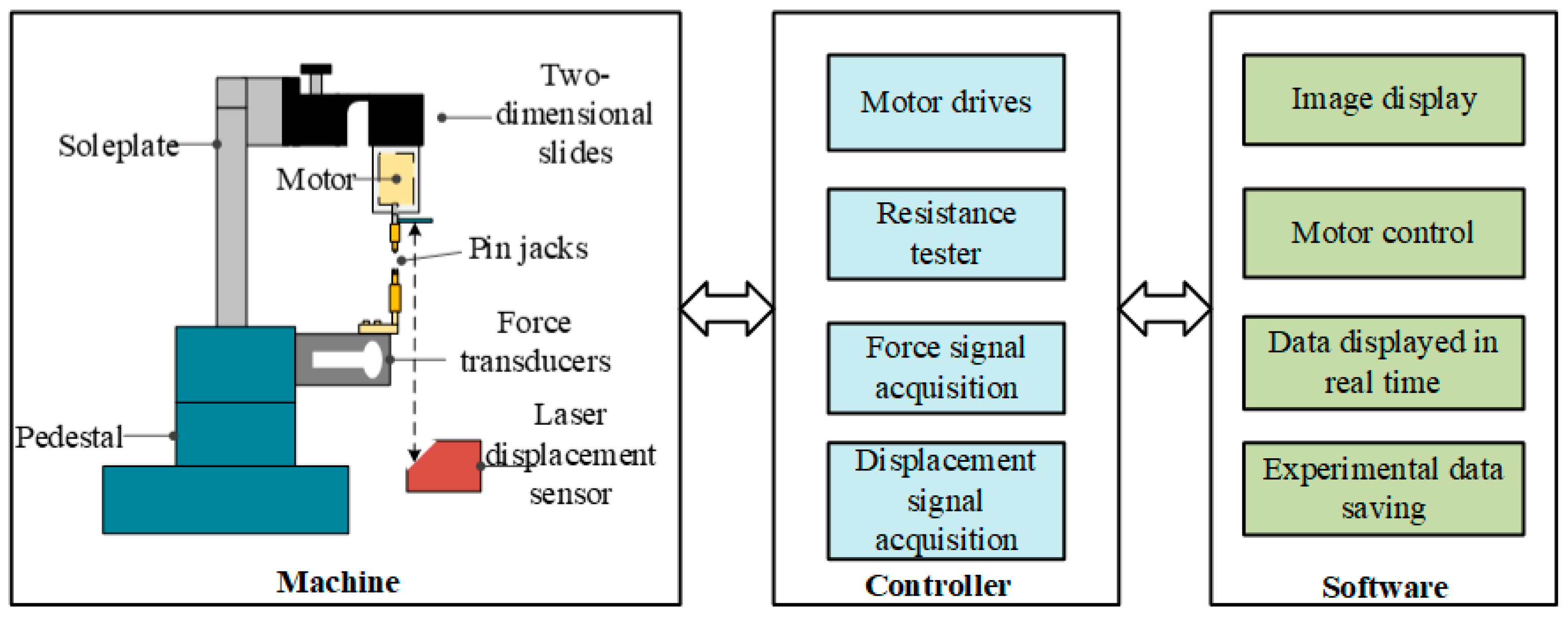
2. Experiment
2.1. Deposition of Au/Ni Layer-by-Layer Coating
2.2. Characterization Techniques
2.2.1. Thickness Test
2.2.2. Corrosion Resistance
2.2.3. Thermal Stability
2.2.4. Insertion–Extraction Tests
3. Results and Discussion
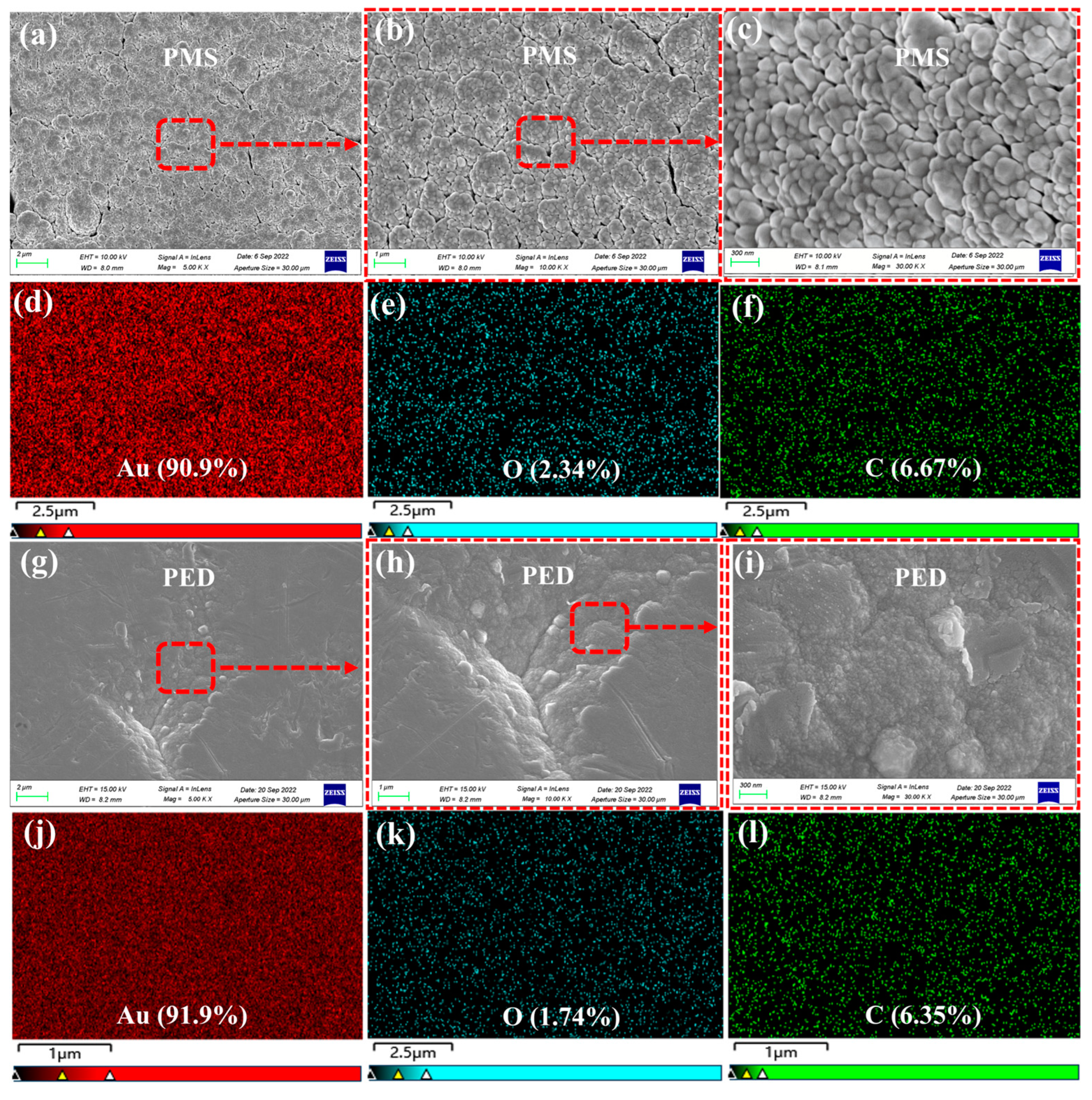
3.1. Surface Quality and Morphology
3.1.1. Macro Surface Quality
3.1.2. Microscopic Surface Quality
3.2. Mechanical Properties of the Coating
3.2.1. Hardness and Elastic Modulus
3.2.2. Analysis of Mechanical Properties
3.3. Evaluation of Insertion–Extraction Behavior
3.4. Wear Mechanism
3.4.1. Wear Phenomenon
3.4.2. Analysis of Wear Mechanism
3.5. Contact Resistance
3.6. Future Studies
4. Conclusions
- (1)
- The coating prepared via magnetron sputtering had a more uniform and denser microstructure than that of the one produced using electroplating, thereby revealing excellent mechanical properties.
- (2)
- The magnetron sputtering process was better able to control the porosity of the coating and enhance its corrosion resistance compared to the electroplating technique.
- (3)
- In combination with microstructure evolution, stress relaxation, and fatigue failure, the main wear mechanism of the electroplated coating was a mixture of abrasive wear, adhesive wear, and localized brittle fracture, while the coating prepared using magnetron sputtering exhibited abrasive wear and localized brittle fracture.
- (4)
- The contact resistance of the pin coated via magnetron sputtering exhibited better stability than the electroplated pin after the repetitive insertion/extraction operations owing to the difference in the microstructure, mechanical properties, and tribological behavior.
Author Contributions
Funding
Institutional Review Board Statement
Informed Consent Statement
Data Availability Statement
Conflicts of Interest
References
- Swingler, J.; McBride, J.; Maul, C. Degradation of road tested automotive connectors. IEEE Trans. Compon. Packag. Technol. 2000, 23, 157–164. [Google Scholar] [CrossRef]
- Xu, L.; Ling, S.; Li, D. Insertion force quality consistency investigation of electrical connector. In Proceedings of the 2016 IEEE 11th Conference on Industrial Electronics and Applications (ICIEA), Hefei, China, 5–7 June 2016; pp. 2395–2399. [Google Scholar]
- El Abdi, R.; Benjemaa, N. Experimental and analytical studies of the connector insertion phase. IEEE Trans. Compon. Packag. Technol. 2008, 31, 751–758. [Google Scholar] [CrossRef]
- Song, J.; Yuan, H.; Koch, C. Accelerated testing of electromechanical connectors considering thermal and mechanical loads. In Proceedings of the 2018 IEEE Holm Conference on Electrical Contacts, Albuquerque, NM, USA, 14–18 October 2018; pp. 467–474. [Google Scholar]
- Kolmer, P.; Shukla, A.; Song, J. Methods of Material and Surface Analysis for the Evaluation of Failure Modes for Electrical Connectors. Technologies 2022, 10, 124. [Google Scholar] [CrossRef]
- 2002/95/EC; Restriction of Hazardous Substances in Electrical and Electronic Equipment. European Commission: Brussel, Belgium, 2003.
- Giurlani, W.; Marcantelli, P.; Benelli, F.; Bottacci, D.; Gambinossi, F.; Passaponti, M.; De Luca, A.; Salvietti, E.; Innocenti, M. Corrosion resistance test of electroplated gold and palladium using fast electrochemical analysis. Coatings 2019, 9, 405. [Google Scholar] [CrossRef]
- Khalakhan, I.; Vorokhta, M.; Chundak, M.; Matolín, V. Au-CeO2 nanoporous films/carbon nanotubes composites prepared by magnetron sputtering. Appl. Surf. Sci. 2013, 267, 150–153. [Google Scholar] [CrossRef]
- Meng, Y.; Ren, W. Investigation on failure mechanism of electrical connectors under repetitive mechanical insertion and withdrawal operations. In Proceedings of the IOP Conference Series: Materials Science and Engineering, Zhengzhou, China, 22–24 October 2021; Volume 1207, p. 012011. [Google Scholar]
- Feng, C.; Lin, X.; Hu, J.; Shen, B.; Hu, Z.; Zhu, F. Study on the influence of fretting wear on electrical performance of SMA connector. Microelectron. Reliab. 2021, 118, 114047. [Google Scholar] [CrossRef]
- Wu, D.Y.; Zhou, X.; Li, L.P.; Ji, C.S.; Wang, X.; Meng, F.S.; Zhai, G.F. Tuning the microstructure, mechanical properties, tribological and electrical contact behavior by Cu doping for gold-based coating. Tribol. Int. 2023, 191, 109193. [Google Scholar] [CrossRef]
- Kannur, K.H.; Yaqub, T.B.; Huminiuc, T.; Polcar, T.; Pupier, C.; Héau, C.; Cavaleiro, A. Synthesis and structural properties of Mo-SN sputtered coatings. Appl. Surf. Sci. 2020, 527, 146790. [Google Scholar] [CrossRef]
- Chen, Z.; Qiao, L.; Hillairet, J.; Song, Y.; Turq, V.; Wang, P.; Laloo, R.; Bernard, J.M.; Lu, K.; Cheng, Y.; et al. Development and characterization of magnetron sputtered self-lubricating Au-Ni/aC nano-composite coating on CuCrZr alloy substrate. Appl. Surf. Sci. 2019, 492, 540–549. [Google Scholar] [CrossRef]
- Coutu, R.; Reid, J.; Cortez, R.; Strawser, R.; Kladitis, P. Microswitches with sputtered Au, AuPd, Au-on-AuPt, and AuPtCu alloy electric contacts. IEEE Trans. Compon. Packag. Technol. 2006, 29, 341–349. [Google Scholar] [CrossRef]
- Yang, Z.; Lichtenwalner, D.J.; Morris, A.S.; Krim, J.; Kingon, A.I. Comparison of Au and Au–Ni alloys as contact materials for MEMS switches. J. Microelectromechanical Syst. 2009, 18, 287–295. [Google Scholar] [CrossRef]
- Liu, Y.C.; Hsiao, S.N.; Chen, Y.H.; Hsieh, P.Y.; He, J.L. High-Power Impulse Magnetron Sputter-Deposited Chromium-Based Coatings for Corrosion Protection. Coatings 2023, 13, 2101. [Google Scholar] [CrossRef]
- Cao, F.; Wang, J.; Lian, Y.; Wang, Y.; Wang, X.; Wang, X.; Song, A.; Shi, L. A Study on the Influence of the Electroplating Process on the Corrosion Resistance of Zinc-Based Alloy Coatings. Coatings 2023, 13, 1774. [Google Scholar] [CrossRef]
- Musil, J.; Kunc, F.; Zeman, H.; Polakova, H. Relationships between hardness, Young’s modulus and elastic recovery in hard nanocomposite coatings. Surf. Coat. Technol. 2002, 154, 304–313. [Google Scholar] [CrossRef]
- Liu, H.-Y. The characteristic research of contact insertion and separation force in connector. In Proceedings of the Thirty-Sixth IEEE Conference on Electrical Contacts, and the Fifteenth International Conference on Electrical Contacts, Montreal, QC, Canada, 20–24 August 1990; pp. 619–624. [Google Scholar]
- Schütz, S.; Suarez, S.; Mücklich, F. Tribo-electric analysis of multi-cycle wear in asymmetric laser-structured Cu-Sn connectors. Tribol. Lett. 2023, 71, 1–12. [Google Scholar] [CrossRef]
- Alderete, B.; Nayak, U.P.; Mücklich, F.; Suarez, S. Influence of topography on electrical contact resistance of copper-based materials. Surf. Topogr. Metrol. Prop. 2023, 11, 025027. [Google Scholar] [CrossRef]


| Test Points | 1 | 2 | 3 | 4 | 5 | AVG | Maximum Deviation |
|---|---|---|---|---|---|---|---|
| PED-Au | 0.54 | 0.67 | 0.96 | 1.17 | 1.31 | 0.93 | 0.77 |
| PED-Ni | 0.48 | 0.64 | 0.78 | 0.83 | 1.03 | 0.752 | 0.55 |
| PED | 1.0 | 1.3 | 1.7 | 2.0 | 2.3 | 1.66 | 1.3 |
| PMS-Au | 1.12 | 1.14 | 1.12 | 1.11 | 1.13 | 1.124 | 0.03 |
| PMS-Ni | 0.85 | 0.86 | 1.02 | 1.03 | 1.06 | 0.964 | 0.21 |
| PMS | 2.0 | 2.0 | 2.1 | 2.1 | 2.2 | 2.08 | 0.2 |
Disclaimer/Publisher’s Note: The statements, opinions and data contained in all publications are solely those of the individual author(s) and contributor(s) and not of MDPI and/or the editor(s). MDPI and/or the editor(s) disclaim responsibility for any injury to people or property resulting from any ideas, methods, instructions or products referred to in the content. |
© 2024 by the authors. Licensee MDPI, Basel, Switzerland. This article is an open access article distributed under the terms and conditions of the Creative Commons Attribution (CC BY) license (https://creativecommons.org/licenses/by/4.0/).
Share and Cite
Zhang, Y.; Zhou, X.; Zhang, Y.; Wu, D.; Wang, X.; Zhai, G. A Study on the Tribological Behaviors of a Pin Coated with Layer-by-Layer Gold/Nickel Materials within an Electrical Connector. Coatings 2024, 14, 170. https://doi.org/10.3390/coatings14020170
Zhang Y, Zhou X, Zhang Y, Wu D, Wang X, Zhai G. A Study on the Tribological Behaviors of a Pin Coated with Layer-by-Layer Gold/Nickel Materials within an Electrical Connector. Coatings. 2024; 14(2):170. https://doi.org/10.3390/coatings14020170
Chicago/Turabian StyleZhang, Yong, Xue Zhou, Yue Zhang, Daoyi Wu, Xu Wang, and Guofu Zhai. 2024. "A Study on the Tribological Behaviors of a Pin Coated with Layer-by-Layer Gold/Nickel Materials within an Electrical Connector" Coatings 14, no. 2: 170. https://doi.org/10.3390/coatings14020170